OB5WPBX-9000-2LWireless PBX Base Unit
Abest Communication Corp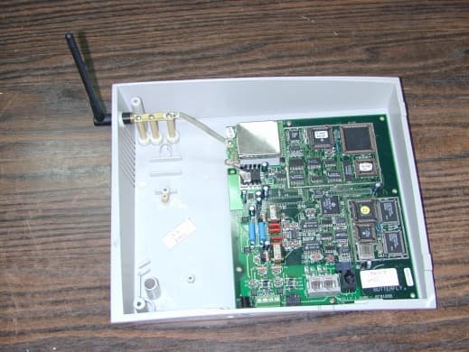
Click to zoom
Application Details
- Equipment Class
- DSS - Part 15 Spread Spectrum Transmitter
- Date of Grant
- Oct 03, 1999
- Application Purpose
- Original Equipment
- Date of Application
- Jul 26, 1999
- Equipment Note
- Wireless PBX Base Unit
- Frequency Range
- 902.50000000 - 927.50000000
- Company
- Abest Communication Corp
- Country
- Taiwan
Documents & Files
Document Text
Text extracted from the exhibit documents filed with the FCC. Open a document above to read the original.
Users Manual
Wireless PBX System Wireless PBX SystemWireless PBX System Wireless PBX System User’s Guide 2Wireless PBX User’s Guide Safety (refer to safety statement at the end of the manual) FCC compliance (refer to FCC statement at the page 6) Product Information (Serial No., Date of Purchase, etc.) Copyright © 1999 by ABEST Communication Corp. Getting Started3 Table of Contents Welcome!.......................................................................................................................8 System box contents...................................................................................................... 9 Getting Started............................................................................................................. 10 Installation ..................................................................................................... 10 Battery information ........................................................................................ 11 Location of controls ....................................................................................... 12 Base unit ...................................................................................... 12 Handset...................................................................................... 13 Making, receiving, and ending calls ............................................................... 14 Making an outgoing call................................................................... 14 Ending a call ................................................................................... 14 Making an internal call..................................................................... 14 Receiving a call ............................................................................... 15 Managing calls .............................................................................................. 15 Transferring a call ........................................................................... 15 Holding a call (Hold exclusive) ........................................................ 15 Call back ...................................................................................... 16 Conference call ............................................................................... 16 Recall (Redial)................................................................................. 17 Recent call ...................................................................................... 17 Picking up a call .............................................................................. 17 Answering a call waiting .................................................................. 18 Phone book.................................................................................................................. 19 Name-recall ................................................................................................... 19 Position-recall................................................................................................ 19 Storing phone numbers ................................................................................. 19 4Wireless PBX User’s Guide Key vs. Letter...................................................................................20 How to enter lower case letters........................................................21 Edit........................................................................................................21 Erase........................................................................................................21 Erase all ........................................................................................................22 Handset programming ..................................................................................................23 Ear volume.....................................................................................................23 Ring volume ...................................................................................................23 Ring type .......................................................................................23 Key tone .......................................................................................23 Key lock ........................................................................................................24 Automatic Key lock ........................................................................................24 Handset PIN (Private Identification Number) ..................................................24 Call forward....................................................................................................25 Do not disturb ................................................................................................25 Phone Lock....................................................................................................25 Hotline........................................................................................................26 Speed dial......................................................................................................26 Dialing.......................................................................................26 Store.......................................................................................26 Call Recording .................................................................................27 System programming ...................................................................................................28 System SIN (System Identification Number) ..................................................28 DIL........................................................................................................28 Music on hold (optional) .................................................................................29 Toll restriction.................................................................................................29 Adding a …
Text truncated - open the document above for the full version.
Block Diagram
FCC ID:OB5WPBX-9000-2L Date: July, 1999 Project number:13306 Page 1 of 2 BLOCK DIAGRAM FCC ID:OB5WPBX-9000-2L Date: July, 1999 Project number:13306 Page 2 of 2 BASE UNIT BLOCK DIAGRAM Base CPU (80930) Flash 128k BFC 2204 SRAM 128k DSP Line Interface Matrix BFC 2201 BFM 9011 J BFM 9021 J BaseBand RF Module X2 (X 4) (X 2) (X 2) TAD DC Power Supply RAD UART Music (Ext/Chip) CODEC Echo Canceller (X 2) RF MODULE AS-239 Antenna BPF RX Data T/R Switch Control Comp Disc LPF DUAL PLL S S BFM 9011 PADriverBuffer OSC TX Data Tune 12MHz 100MHz 10.7MHz Ceramic 110.7MHz SAW 915MHz SAW 915MHz Ceramic Digital Control LNA BPF BPF BPF Limitter S BFM 9021 TX enable RX enable Ceramic 90
Cover Letter(s)
ABEST COMMUNCATION CORP. 19-7 Ting-Tien-Liao, Hsien-Jenli, Tel: 886-2-26237902 2623-7903 Tamsui, Taipei, Taiwan, R.O.C. Fax: 886-2-2621-7261 July 26, 1999 FEDERAL COMMUNICATIONS COMMISSION EQUIPMENT APPROVAL SERVICES P.O.B. 358315 Pittsburgh, PA 15251-5315 USA Subject: Application for certification of wireless PBX base unit (hopping transceiver), FCC ID:OB5WPBX-9000-2L Dear Gentlemen, Please find attached our application for certification of wireless PBX base unit (hopping transceiver), model WPBX-9000-2L, FCC ID: OB5WPBX-9000-2L, prepared in accordance with FCC Rules, parts 2 and 15. The product testing and this application for certification were performed by Hermon Laboratories, which is listed by FCC. Hermon Labs responsible person is Dr. Edward Usoskin, tel: 01197266288001, fax:01197266288277, e-mail: [email protected]. We hope this application satisfies your requirements. Sincerely yours, Jason Chen, product manager ABEST COMMUNCATION CORP.
External Photos
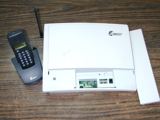
FCC ID:OB5WPBX-9000-2L Date: July, 1999 Project number:13306 Page 1 of 3 EXTERNAL PHOTOS Contain 2 pages follow this page FCC ID:OB5WPBX-9000-2L Date: July, 1999 Project number:13306 Page 2 of 3 Photograph No.1 WPBX-9000 system (base unit and handset) general view FCC ID:OB5WPBX-9000-2L Date: July, 1999 Project number:13306 Page 3 of 3 Photograph No.2 WPBX-9000-2L transceiver with antenna and screen
ID Label/Location Info
FCC ID:OB5WPBX-9000-2L Date: July, 1999 Project number:13306 Page 1 of 1 LABEL The label shown below is affixed on the bottom of WPBX-9000-2L base unit This device complies with FCC Rules Part 15 and Part 68. FCC REGISTRATION No.:______________ REN: _______________ Jack : RJ11C Serial No.: ____________ Operation is subject to the following two conditions: (1) This device may not cause harmful interference and (2) This device must accept any interference received including interference that may cause undesired operation. FCC ID:OB5WPBX-9000-2L Model No.: WPBX-9000 ABEST COMMUNICATIONS CORP. MADE IN TAIWAN
ID Label/Location Info
FCC ID:OB5WPBX-9000-2L Date: July, 1999 Project number:13306 Page 1 of 2 LABEL The label shown below is affixed on the bottom of WPBX-9000-2L base unit as shown in the sketch, page 2. This device complies with FCC Rules Part 15 and Part 68. FCC REGISTRATION No.:______________ REN: _______________ Jack : RJ11C Serial No.: ____________ Operation is subject to the following two conditions: (1) This device may not cause harmful interference and (2) This device must accept any interference received including interference that may cause undesired operation. FCC ID:OB5WPBX-9000-2L Model No.: WPBX-9000 ABEST COMMUNICATIONS CORP. MADE IN TAIWAN FCC ID:OB5WPBX-9000-2L Date: July, 1999 Project number:13306 Page 2 of 2 Base unit general view Bottom Label placement on the EUT bottom Antenna PABX Base Label
Internal Photos
FCC ID:OB5WPBX-9000-2L Date: July, 1999 Project number:13306 Page 1 of 4 INTERNAL PHOTOS Contain 3 pages follow this page FCC ID:OB5WPBX-9000-2L Date: July, 1999 Project number:13306 Page 2 of 4 Photograph No.1 WPBX-9000-2L motherboard with transceiver (under screen) FCC ID:OB5WPBX-9000-2L Date: July, 1999 Project number:13306 Page 3 of 4 Photograph No.2 WPBX-9000-2L transceiver PCB view FCC ID:OB5WPBX-9000-2L Date: July, 1999 Project number:13306 Page 4 of 4 Photograph No.3 WPBX-9000-2L transceiver PCB rear side view
Operational Description
FCC ID:OB5WPBX-9000-2L Date: July, 1999 Project number:13306 Page 1 of 2 OPERATIONAL DESCRIPTION FCC ID:OB5WPBX-9000-2L Date: July, 1999 Project number:13306 Page 2 of 2 SYSTEM DESCRIPTION The wireless PBX uses a spread spectrum frequency hopping RF link to transfer control data and digital compressed voice at a bit rate of approximately 115Kbit/sec in each direction. PBX features such as digital voice data switching, CO lines interface control and extension controls are all done at the base module. System basic configuration is done from the handsets. The Base unit manages the Handsets (Data and control). It acts as two CO lines interface and perform all PBX function. Other system options are two additional CO lines interface and TAD. Following, a short description of the block diagram: • Base CPU - The 80930 processor communicates over the WINGS TM network utilizing a coprocessor as RF controller (BFC2204). It manages all PBX functions (switching, etc.), handles the CO lines interface, controls the analog matrix, and handles the DSPs (up to four CO lines, two analog matrixes and four DSPs, operating with the additional configuration). It also controls a TAD, telephone answering device (when options assembled in any configuration). For maximum performance the 80930 runs in Page-mode with zero wait-states (see also base memory description). • RF Module – Based on the Butterfly’s MMIC BFM9011J and BFM9021J for 900MHz SSFH. • Base Band – BFC2201 net controller and BFC2204 RF controller. • Memory – 128K bytes SRAM with 25nS access time and 128K bytes with 90nS access time Flash memories, are used to run the 80930 in Page-mode with zero wait-states performing a bootstrap mechanism (see section 2.3) at power-up. Large SRAM with a non-volatile Flash memory allows an easy maintenance for features such as phone-book and software upgrade. • DSP’s – CT8015 TrueSpeech ® DSPs (up to four DSPs for four CO lines). • Matrix – 8 x 16 analog matrix (up to two analog matrixes for four CO lines) for switching and conferencing. • Line interfaces – CO line interface circuit (up to four CO lines), with echo canceller of 64mS for each line, Caller ID type II decoders, DTMF receivers, call progress detection, one POTS connection per system. • DC – 9 volts 1 Amp transformer regulated and filtered to 5 volts. RF module uses separate regulator and set of filters. Additional minus 5 volts converter is used to operate OpAmps. • TAD – to be defined. FCC ID:OB5WPBX-9000-2L Date: July, 1999 Project number:13306 Page 3 of 2 General The transmitter and receiver in the RF module share a single antenna terminal which is switched between them on a TDD basis (time division duplex), i.e., when a data packet is received the transmitter is inactive and does not interfere with the reception, and the reception is inactive during transmissions. The transceiver employs frequency hopping spread spectrum which is managed by the baseband processor (external to the RF module). The transmission and reception are based on synthesized oscillators that share the same 12 MHz reference clock which is provided as an input to the module. • Carrier Frequencies The transceiver’s 50 frequencies are: 902.5MHz, 903.0MHz, 903.5MHz...927.0MHz (902.5MHz to 927.0MHz with 0.5MHz channel separation). • Modulation and Bandwidth The modulation index of the FSK modulation is set to h≅0.5, which creates a modulated signal with a 20dB bandwidth of about 500kHz (maximum allowed by the FCC in this frequency band). Receiver The receiver is a dual conversion heterodyne receiver with a second IF at 10.7 MHz, where the FSK demodulation is performed. Its circuitry is based on the BFM9021J incorporating a low-noise- amplifier, two frequency conversions, an FM demodulator and an RSSI output (received signal strength indication). An external baseband stage functions as a data slicer and provides a logic- level output which is interfaced with the digital logic external to the module. The first conversion is based on a synthesized local oscillator which is set at 110.7 MHz above the received frequency (the first IF is at 110.7MHz). The second conversion is based on a fixed crystal oscillator at 100MHz which down-converts the modulated signal to the second IF of 10.7MHz. The receiver sensitivity for a bit error rate (BER) of 10 -5 is about –93dBm. Transmitter The transmitter is based on the BFM9011 IC, which incorporates the modulator and the power amplifier. The transmission power may be adjusted externally between a few power levels reaching a maximum of about 20dBm (100mW). The RF oscillator runs at the carrier frequency and is frequency modulated directly by the data signal while the synthesizer loop is disabled. FCC ID:OB5WPBX-9000-2L Date: July, 1999 Project number:13306 Page 4 of 2 Frequency Hopping Communications Parameters in the WPBX- 9000 Scope & Purpose This document specifies some of the frequency hopping communication parameters of the wireless PBX WPX-9000, and is intended to provide proof of its compliance with FCC Part 15.247 requirements. The chipset on which the product is based implements the WiNGs wireless protocol (Wireless Indoor Network – a Generic Solution) developed by Butterfly Communications (now the Short Distance Wireless Division of Texas Instruments). The communications protocol and other technical details regarding the chipset implementing it can be found at: www.Butterfly.com. Hopping Sequences The frequency hopping communications in the WPBX-9000 is based on a periodic use of 25 frequencies, which are selected at system initialization according to environmental occupancy. This is the minimal number of frequencies required for systems transmitting up to 0.25W (the transmission power in the WPBX-9000 is 100mW). The order of appearance of the selected frequencies is randomized and scrambled to obtain a pseudo-random pattern, as required in section 15.247. In addition, this ensures that other systems of this type, which might be using the sa…
Text truncated - open the document above for the full version.
Schematics
A A B B C C D D E E 44 33 22 11 PC-0124 C APOLLO - RF Texas Instruments (Israel) Short Distance Wireless Business Unit Tel: +972-9-747-6969, Fax: +972-9-743-0951 C 13Sunday, June 13, 1999 P.O.Box 5133 Kfar Saba 44150 ISRAEL Title SizeDocument NumberRev Date:Sheet of Name Date Sign Designer Approval Chief Eng. Eng.Mang. This publication contains proprietary information of Texas Instruments. and may not be disclosed to others without the written permission of Texas Instruments. Preliminary evaluation schematics. Circuit and values are subject to change without notice. HAND-SET SYNDT SYNLESYNCLK TXPWR1 TXPWR0 TXOSCEN -RXOSCEN TXEN -RFMEN REFCLK TXD RXD LO-SAMP PWR-LEVEL LO-SAMP 12MHz-CLK TX-OSC-OFF SYNT_CLK PWR_MSB SYNT_CLK SYNT_STB OSC-ENABLE PWR_MSB PWR-LEVEL PWR_LSB R-SW R-SW OSC-ENABLE TX-OSC-ON TXDATA TXDATA TX-OSC-ON TX-OSC-ON Vtx -RF_ENABLE -RF_ENABLE-RF_ENABLE RXDATA RXDATA 12MHz SYNT_DATA SYNT_DATA SYNT_CLK TXDATA T-SW TX-OSC-OFF OSC-ENABLE RXDATA SYNT_STB SYNT_DATA PWR_MSB -RF_ENABLE 12MHz PWR_LSB PWR_LSB Vin_BAT T-SW T-SW T-SW Vin_BAT 3V-RF 3V-RF 3V-RF Vtx Vtx Vin_BAT 3V-RF 3V-RF 3V-RF 3V-RF Vin_BAT 3V-RF Vin_BAT 3V-RF 3V-RF Vin_BAT 3V-RF 3V-RF Vin_BAT 1 1 1 1 1 1 1 11 1 1 1 1 1 1 1 1 1 1 1 1 1 1 1 1 1 1 11 1 1 1 1 1 1 1 1 1 1 11 1 1 1 1 1 1 1 1 11 1 1 1 1 1 1 1 1 1 1 1 1 1 1 1 1 1 11 1 1 1 1 1 1 1 1 1 11 1 1 1 1 11 ANT1 ANTENNA TP1 FLT4 SFE10.7MA21-SIP3 IN 1 GND 2 OUT 3 U8A MC34072D-SO8 + - 3 2 1 8 4 U9 TK11330-SOT23L Control 1 GND 2 Noise Bypass 3 Vout 4 GND 5 Vin 6 TP2 FLT6 SAFU110.6MSA40T RFIN 10 GND 9 RFOUT 5 GND 2 GND 1 GND 3 GND 8 GND 4 GND 7 GND 6 TP3 TP6 U8B MC34072D-SO8 + - 5 6 7 8 4 TP4 TP5 FLT7 LFL30-12C0915B026 NC2 1 IN 10 NC1 2 OUT 5 GND 3 NC2 4 NC2 6 NC1 7 GND 8 NC2 9 TP7 D2 SMV1104-50 D1 SMV1104-50 J2 N.C.-HEADER2X2-F 12 34 U5 WB1315X-SSOP20 VCC1 1 VP1 2 D01 3 GND 4 FIN1 5 FIN1 6 GND 7 OSC-IN 8 CLK 11 DATA 12 LE 13 FIN2 16 GND 17 D02 18 VP2 19 VCC2 20 FIN2 15 GND 14 GND 9 FoLD 10 J1 HEADER2X8-F 12 34 56 78 910 1112 1314 1615 U10 AS125-73 J3 1 GND 2 J1 3 J2 4 V2 5 V1 6 D3 BAT 64-04 12 3 Q7 BC857 1 2 3 U1 BFM9011J VCC3 1 GAINctrl 2 GND 3 GND 7 GND 8 GND 4 GND 5 IPAout 6 PAout 9 GND 10 GND 11 VCC4 12 PAenable 13 GND 14 GND 15 MODenable 16 GND 17 GND 19 GND 21 VCC1 22 VCC2 24 GND 25 GND 27 PAin 28 MODout 26 OSCsmp 23 TANK 20 MODin 18 U6 BFM9021J LNAin 1 GND 2 LNAout 3 MIX1in 5 MIX1out 6 GND 7 MIX2in 8 MIX2out 9 GND 10 GND 4 LIMin 11 LIMdec1 12 LIMdec2 13 RSSI 14 QUADin 15 LIMout 16 VCC3 17 DETout 18 OSC2emit 19 OSC2base 20 OSCsmp 21 VCC2 22 TANK 23 GND 24 VCC1 25 LNAdec 26 Atten 27 ENABLE 28 C91 10nF C38 0.1uF C61 1nF C86 N.C. C41 0.1uF C83 10pF C88 N.C. C39 100pF C85 10nF C12.7pF C7 33pF C69 33pF C47 100pF C77 12pF C10 100pF C40 100pF C9 100pF C35 100pF C80 1nF C49 100pF C113 33pF C8 1nF C18 N.C. C20 N.C. C45 100pF C29 1uF C11 1nF C14 N.C.-27pF C116 33pF C11133pF C82 4.7nF C84 15pF C81 4.7nF C52 330pF C3100pF C62 100pF C43 33nF C63 100pF C54 100pF C60 10nF C56 100pF C37 1nF C114 33pF C53 100pF C107 33pF C5 100pF C108 33pF C6 100pF C36 100pF C31 0R C1533.9pF C102 33pF C103 33pF C11233pF C94 33pF C97 33pF C101 N.C. C26 100pF C76 N.C. C117 33pF C120 0.5pF C51 100pF C92 0.1uF C121 100pF C99 0.1uF C104 0.1uF C110 470pF C100 100pF C105 100pF C4 N.C. C55 100pF C128 8.2pF C129 8.2pF C22 2.7pF C130 1nF C93 0.1uF C150 10nF C151 0.5pF C119 N.C.C152 N.C. C13 N.C. C154 100pF C155 10nF C156 100pF C2 2.2uF C48 1.5nF-COG C125 N.C. C106 2.2uF C98 100uF CDA10.7MG15-SIP2 U11 IN 1 OUT 2 XT1 100MHz-50ppm-LP 1 23 4 FLT2 F5CH-900M-L2 GND 1 IN 2 GND 3 GND 4 GND 6 OUT 5 L422nH L222nH L11.5nH L1122nH L19 N.C. L17 12nH-2% L20 10nH-2% L24 12nH L25 0H-0R L26 22nH LB1 1uH L27 6.8nH L28 6.8nH L12 560nH L13 120nH L21 180nH L22180nH L23 N.C. R11 3.2k R10 N.C. R12 10R R20 68k R3 10k R25 10k R13 51R R5 10k R16 1.5k R4 N.C. R22 51R R29 470R R38 3k R28 3.6k R42 100k R24 6.2k R44 0R R1 N.C. R43 N.C. R47 N.C. R48 N.C. R51 10k R33 51k-1% R37 10k R39 82k R35 N.C. R53 N.C. R40 0R R2N.C. R628.2k R18 N.C. R19 N.C. R54 N.C. R30 470R R63 22k R9 3.2k R68 10k R66 0R R67 N.C. R152 N.C. R151 10R R155 N.C. R45 N.C. R154 3.9k R36 300R R150 N.C. R61 3.3k R153 2.4k R49 0R R64 N.C. R156 220k R157 220k R158 5.1k R159 51k-1% R161 10k R160120R R162 10k R163 2.2k R164 10k R41 10k Q5 MMBT2222A 1 2 3 A A B B C C D D E E 44 33 22 11 2 4 5 hold 17 80 * menu 1 5 VLCD yes flash 6 3 no #9 Line redial RINGER LCD_CON PC-0124 C HAND SET USER Texas Instruments (Israel) Short Distance Wireless Business Unit Tel: +972-9-747-6969, Fax: +972-9-743-0951 Custom 23Sunday, June 13, 1999 P.O.Box 5133 Kfar Saba 44150 ISRAEL Title SizeDocument NumberRev Date:Sheet of Name Date Sign Designer Approval Chief Eng. Eng.Mang. This publication contains proprietary information of Texas Instruments. and may not be disclosed to others without the written permission of Texas Instruments. RINGER D[0:7] SDA SCL RINGER D[0:7] ROW[1:3] D6 D5D4D3D2D1 D0 SDA SCL ROW3 ROW[1:3] ROW1 ROW2 LCD_DATA LCD_CLK D[0:7] RINGER ROW[1:3] 3V 3V 111 1 CE24 15nF RE35 20R RE43 10k QE4 BC857 1 2 3 RE41 1k CE25 0.1uF JE9 HEADER1X5 1 2 3 4 5 JE8 HEADER1X2 1 2 RE42 1k SE13 SWITCH RE37 1k RE39 1k RE40 1k RE36 1k RE38 1k SE7 SWITCH SE17 SWITCH LE3 20nH CE37 33pF TPE50 BUZZER TPE58 TP-PAD TPE72 SCL TPE73 SCA TPE74 VCC TPE75 VSS TPE76 VLCD TPE51 TPE59TPE60TPE61TPE62TPE63TPE64 TPE65 TPE66 TPE83 TPE82TPE81TPE80TPE79TPE78TPE77 TPE94TPE93TPE92TPE91TPE90TPE89 SE3 SWITCH SE2 SWITCH SE14 SWITCH SE10 SWITCH SE11 SWITCH SE19 SWITCH SE5 SWITCH SE6 SWITCH SE15 SWITCH SE1 SWITCH SE9 SWITCH SE8 SWITCH SE12 SWITCH SE16 SWITCH SE4 SWITCH SE18 SWITCH A A B B C C D D E E 44 33 22 11 NET ALIAS FROM APPLICATION TO BFC2203 REFER TO APPLICATION. NET ALIAS FROM DSP TO CODEC REFER TO DSP. ESD PROTECTION * PLACE NEAR U4/PIN 3 AND PIN 20 * DEBUG_CON NETWORK CON GND TO AGND CONNECTION This publication contains proprietary information of Butterfly Communications Inc. and may not be disclosed to others without the written permission of Butterfly Communications Inc. PC-0124 C HAND SET USER Texas Instruments (Israel)…
Text truncated - open the document above for the full version.
Test Report
Test Report: ABEFCC.13306.doc Date: June, 1999 FCC ID: OB5WPBX-9000-2L Page 1 of 63 HERMON LABORATORIES ELECTROMAGNETIC EMISSIONS TEST REPORT according to FCC Part 15 subpart C, §15.247 and subpart B for ABEST COMMUNICATION CORP. EQUIPMENT UNDER TEST: Wireless Multi-Handset System (PBX) Base Unit FCC ID: OB5WPBX-9000-2L Prepared by: ___________ Mrs. M. Cherniavsky, cert. engineer Hermon Labs Approved by: _________________ Mr. A. Usoskin, QA manager Hermon Labs Approved by: _________________ Mr. Jason Chen, product manager ABEST Communication Corp. Hermon Laboratories Ltd. P.O.Box 23 Binyamina 30550, Israel Tel.+972-6628-8001 Fax.+972-6628-8277 Email:[email protected] Electrical Test Report: ABEFCC.13306.doc Date: June, 1999 FCC ID: OB5WPBX-9000-2L Page 2 of 63 HERMON LABORATORIES Description of equipment under test Test itemsBase unit frequency hopping transceiver FCC ID:OB5WPBX-9000-2L ManufacturerABEST .Communication Corp. Brand markABEST Apollo Types (Models)WPBX-9000-2L Receipt dateFebruary 22, 1999 Applicant information Applicant’s representativeMr. Oren Eliezer, chief engineer Applicant’s responsible personMr. Jason Chen, product manager CompanyABEST .Communication Corp. Address19-7 Ting-Tien-Liao, Hsien-Jenli Postal code CityTamsui, Taipei CountryTaiwan, R.O.C. Telephone number+886 2 2623 7902 Telefax number +886 2 2621 7261 Test performance Project Number:13306 LocationHermon Laboratories Test startedFebruary 22, 1999 Test completedFebruary 25, 1999 Purpose of testThe EUT certification in accordance with CFR 47, part 2, §2.1033 Test specification(s)FCC Part 15, Subpart C, §15.247, §§15.205, 15.207, 15.209, 15.107, 15.109 The A2LA logo endorsement applies only to the test methods and the standards that are listed in the scope of Hermon Laboratories accreditation by A2LA Through this report a point is used as the decimal separator and the thousands are counted with a comma. This report is in conformity with EN 45001 and ISO GUIDE 25. The test results relate only to the items tested. This test report must not be reproduced in any form except in full, with the approval of Hermon Laboratories Ltd. Test Report: ABEFCC.13306.doc Date: June, 1999 FCC ID: OB5WPBX-9000-2L Page 3 of 63 HERMON LABORATORIES Table of Contents 1GENERAL INFORMATION..........................................................................................................4 1.1ABBREVIATIONS AND ACRONYMS.................................................................................................4 1.2SPECIFICATION REFERENCES........................................................................................................5 1.3EUT DESCRIPTION......................................................................................................................5 1.4CHANGES MADE IN EUT..............................................................................................................6 1.5EUT TEST CONFIGURATION.........................................................................................................7 2TEST FACILITY DESCRIPTION.................................................................................................9 2.1GENERAL....................................................................................................................................9 2.2EQUIPMENT CALIBRATION...........................................................................................................9 2.2.1Expanded uncertainty at 95% confidence in Hermon Labs EMC measurements...............10 2.3LABORATORY PERSONNEL.........................................................................................................10 2.4STATEMENT OF QUALIFICATION.................................................................................................11 3EMISSION MEASUREMENTS...................................................................................................12 3.1FREQUENCY HOPPING CHANNELS SEPARATION AND HOPPING FREQUENCY USAGE TEST ACCORDING TO §15.247(A)(1)(I)..............................................................................................................................12 3.1.1Definition of the test.........................................................................................................12 3.1.2Test set-up........................................................................................................................12 3.1.3Test results.......................................................................................................................12 3.2OCCUPIED BANDWIDTH TEST ACCORDING TO § 15.247(A)(1)(I)...................................................14 3.2.1Definition of the test.........................................................................................................14 3.2.2Test set-up........................................................................................................................14 3.2.3Test results.......................................................................................................................14 3.3AVERAGE TIME OF OCCUPANCY DEFINITION ACCORDING TO § 15.247(A)(1)(I)..............................18 3.3.1Definition.........................................................................................................................18 3.3.2Calculation......................................................................................................................18 3.4MAXIMUM PEAK OUTPUT POWER TEST ACCORDING TO §15.247 (B)(2)..........................................21 3.4.1Definition of the test.........................................................................................................21 3.4.2Test set-up........................................................................................................................21 3.4.3Test results.......................................................................................................................21…
Text truncated - open the document above for the full version.
Contact Information
Applicant
Jason Chen(Manager)
886-2-2621-7902Fax: 886-2-2622-0674
Technical Contact
Hermon LaboratoriesEdward Usoskin
[email protected]011 972 6628 8001
HaRakevet Industrial Zone · Binyamina · Israel
Non-Technical Contact
Texas Instruments Israel Ltd.Oren Eliezer
[email protected]011 972 9747 6969
Test Firm
Hermon Laboratories Ltd.Alexander Usoskin
Technical Specifications
| # | Rule Parts | Frequency Range | Power Output |
|---|---|---|---|
| 1 | 15C | 902.5 MHz - 927.5 MHz | 100.00 mW |
Other Applications from Abest Communication Corp
OB5WPBX-9000-H
Nov 03, 1999DSS - Part 15 Spread Spectrum Transmitter
Equipment Class
DSS - Part 15 Spread Spectrum Transmitter
OB5DSS-2000
Jun 20, 1999Cordless Telephone
Equipment Class
DSS - Part 15 Spread Spectrum Transmitter