OJGFE51214888AF55GSM Mobile Phone
5cell(HK)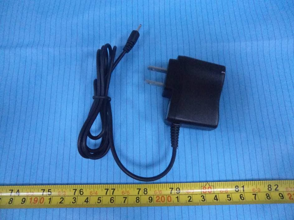
Click to zoom
Application Details
- Equipment Class
- PCE - PCS Licensed Transmitter held to ear
- Date of Grant
- Jul 13, 2012
- Application Purpose
- Original Equipment
- Date of Application
- Jul 13, 2012
- Equipment Note
- GSM Mobile Phone
- Frequency Range
- 1850.20000000 - 1909.80000000
- Company
- 5cell(HK)
- Country
- Hong Kong
Documents & Files
Document Text
Text extracted from the exhibit documents filed with the FCC. Open a document above to read the original.
Users Manual
e 700 User Manual I Contents 1.Getting to know your phone ............................1 1.1 Your Phone ..................................................1 1.2 Status icons..................................................1 1.3 Installing SIM card and battery.....................1 1.4 Installing Storage card .................................2 1.5 Battery charging...........................................2 1.6 Power on/ off................................................3 1.6.1 Power on ...............................................3 1.6.2 Power off ...............................................3 1.7 Using shortcut keys......................................3 2.Using Call Function..........................................4 2.1 Making a call ................................................4 2.1.1 Directly call on Home Screen ................4 2.1.2 Make an international call......................4 2.2 Answering or rejecting a call ........................4 2.2.1 Answer a call .........................................4 2.2.2 Reject a call...........................................4 2.3 Adjusting call volume ...................................4 2.4 Ending a call ................................................4 3.Call logs ............................................................5 3.1 Dialed calls...................................................5 3.2 Received call................................................5 3.3 Missed call ...................................................5 3.4 Rejected call ................................................5 3.5 Delete all ......................................................5 3.6 Call timers ....................................................5 3.7 Call cost .......................................................5 3.8 GPRS counter..............................................5 4.Profiles.............................................................. 6 4.1 General........................................................ 6 4.2 Vibrate ......................................................... 6 4.3 Outdoor ....................................................... 6 4.4 Indoor .......................................................... 6 4.5 Meeting........................................................ 6 5.Contacts............................................................ 7 5.1 View a contact ............................................. 7 5.2 Adding a new contact .................................. 7 6.Messages.......................................................... 8 6.1 Write message............................................. 8 6.1.1 New SMS .............................................. 8 6.1.2 New MMS ............................................. 8 6.2 Inbox............................................................ 8 6.3 Outbox......................................................... 8 6.4 Drafts ........................................................... 8 6.5 Sentbox ....................................................... 8 6.6 Message setting .......................................... 8 6.6.1 Templates.............................................. 8 6.6.2 Voice mail server................................... 8 6.6.3 Broadcast message .............................. 9 6.6.4 SMS settings......................................... 9 6.6.5 MMS settings ........................................ 9 6.6.6 Message capacity ............................... 10 7.Internet............................................................ 11 7.1 Input URL ...................................................11 7.2 Homepage ..................................................11 7.3 Bookmark ...................................................11 II 7.4 History ....................................................... 11 7.5 Offline ........................................................ 11 7.6 WAP settings ............................................. 12 7.6.1 Browser settings.................................. 12 7.6.2 Network account ................................. 12 7.6.3 Preferred storage ................................ 12 7.6.4 Restore default.................................... 12 8.Multimedia ...................................................... 13 8.1 Camera...................................................... 13 8.2 Video recorder ........................................... 13 8.3 Audio player............................................... 13 8.3.1 Background audio player .................... 13 8.4 Video player............................................... 13 8.5 Image browser ........................................... 14 8.6 Recorder.................................................... 14 8.7 FM radio .................................................... 14 8.8 File manager.............................................. 14 9.Tools................................................................ 15 9.1 Alarm ......................................................... 15 9.2 Calendar .................................................... 15 9.3 Calculator .................................................. 15 9.4 E-Book reader ........................................... 15 9.5 Bluetooth ................................................... 15 9.6 Sokoban .................................................... 16 10.Settings ......................................................... 17 10.1 Dual-SIM.................................................. 17 10.2 Call setup................................................. 17 10.2.1 Network selection.............................. 17 10.2.2 Call divert .......................................... 17 10.2.3 Call barring........................................ 18 10.2.4 Call waiting ........................................19 10.2.5 Hide ID...............................................19 10.2.6 Select line ..........................................19 10.2.7 Flight mode ........................................19 10.2.8 Others.........…
Text truncated - open the document above for the full version.
External Photos
EXHIBIT B - EUT EXTERNAL PHOTOGRAPHS EUT– Front View EUT– Rear View EUT – Side View 1 EUT – Side View 2 EUT – Adapter View EUT – Adapter Label View
ID Label/Location Info
EXHIBIT A - FCC ID LABELING AND LOCATION FCC ID Label FCC ID Label Location Label here The label shown shall be permanently affixed at a conspicuous location on the device and be readily visible to the user at the time purchase (Labeling requirements per 2.925)
Internal Photos
EXHIBIT C - EUT INTERNAL PHOTOGRAPHS EUT – Battery off View EUT – Cover off View GSM Antenna Location BT Antenna Location EUT – Main Board with LCD and Keyboard View EUT – Main Board with Keyboard View EUT – Main Board Top View EUT – Main Board Bottom View EUT – Main Board Bottom Shielding off View EUT – LCD Top View EUT – LCD Bottom View EUT – Battery View
Operational Description
This project integrates basebandand RF module N700_MB_V0.6,The module is mounte dasapart of this project with the PCBA. 1. RFPA and antenna switch SCH(page4) The aerial signal mobile phone received goes from GSM_ANT to RF Connector J403.RF Connector is a special parts developed for RF test. By connecting RF cable to spectrum analyzer, you can measure RF signal.Signal output from RF Connector will be input to GSM quad band front-end module U402 (integratedwithRFPA). CPU output signals to the ports of U403,such as CPCTL0, CPCTL1,and TX_EN . TX_EN will be incharge of GSM quad band front-end module U403, in relative Band (GSM850、GSM900、DCS1800、PCS1900) and in TX/RX or standby status as belowfigure. 2. RX SAW Filter SCH (page4) The RX signal output from RF SW,than input SAWfilter.changed two difference signal sin SAWfilter, than input the transceiver of U404(QS518). 3. The RF overall schematic as “7203-CIRCUIT FOR N700” page 4. It contains the TX pathand RX path.The signal received rom the air will be demodulated in CPU through RX SAW and Transceiver,Then the original voice signal will driver the receiver. At the sametime the signal from microphone will be sent to transceiver through , then be amplified by RFPA, at last sent to air from the antenna switch. 4 BT partschematic (page12) The Blue tooth over all schematic as up.RDA5872 is a highly integrated Bluetooth IC,which is compliant with Bluetooth2.0 specification an dprovides an optimal solution for data and voice application. It includes powerfull processing capabilities with rich features and a high performance transceiver, all in a compact single package.
Parts List/Tune Up Info
NO. STAT E PART NO. DESCRIPTION UNIT NUM REF 1 P H-0502-000JB0-B00 Resistor,0 ohm,±5%,1/16W,0402 PCS 20 C419,C1319,R522,R527,R656,R620,R1201,R1301,R1320,R1325,R1340,R910,B904,B905,R951,R952,R1213,R1214,R1215,R1202 2 P H-0502-000JF0-C00 Resistor,0 ohm,±5%,1/10W,0603 PCS 2 R940,R945 3 P H-0502-036FE0-D00 Resistor,0.36 ohm,±1%,1/4W,0805 PCS 1 R300 4 P H-0502-100JB0-B00 Resistor,10 ohm,±5%,1/16W,0402 PCS 2 R303,R1114 5 P H-0502-330JB0-B00 Resistor,33 ohm,±5%,1/16W,0402 PCS 19 R202,R203,R410,R901,R902,R903,R904,R905,R1302-R1312 6 P H-0502-101JB0-B00 Resistor,100 ohm,±5%,1/16W,0402 PCS 2 R600,R604 7 P H-0502-221JB0-B00 Resistor,220 ohm,±5%,1/16W,0402 PCS 12 R1007-R1 018 8 P H-0502-471JB0-B00 Resistor,470 ohm,±5%,1/16W,0402 PCS 2 R1315,R13 16 9 P H-0502-511JB0-B00 Resistor,510 ohm,±5%,1/16W,0402 PCS 1 R412 10 P H-0502-102JB0-B00 Resistor,1K ohm,±5%,1/16W,0402 PCS 19 R2,R231,R405,R406,R407,R408,R601,R605,R606,R615,R941,R942,R1004,R1113,R1134,R1321,R1322,R1323,R1324 11 P H-0502-152JB0-B00 Resistor,1.5K ohm,±5%,1/16W,0402 PCS 3 R208,R6 08,R609 12 P H-0502-202JB0-B00 Resistor,2K ohm,±5%,1/16W,0402 PCS 4 R500,R614 ,R802,R803 13 P H-0502-512JB0-B00 Resistor,5.1K ohm,±5%,1/16W,0402 PCS 2 R502,R1 203 14 P H-0502-622FB0-B00 Resistor,6.2K ohm,±1%,1/16W,0402 PCS 1 R201 15 P H-0502-103JB0-B00 Resistor,10K ohm,±5%,1/16W,0402 PCS 7 R206,R40 3,R520,R523,R655,R1326,R1327 16 P H-0502-153JB0-B00 Resistor,15K ohm,±5%,1/16W,0402 PCS 1 R401 17 P H-0502-203JB0-B00 Resistor 20K ohm,±5%,1/16W,0402 PCS 4 R621,R62 2,R651,R652 18 P H-0502-473JB0-B00 Resistor,47K ohm,±5%,1/16W,0402 PCS 4 R623,R65 3,R1115,R1116 19 P H-0502-753JB0-B00 Resistor,75K ohm,±5%,1/16W,0402 PCS 2 R624,R65 4 20 P H-0502-104JB0-B00 Resistor,100K ohm,±5%,1/16W,0402 PCS 2 R1133,R 1319 21 P H-0502-154JB0-B00 Resistor,150K ohm,±5%,1/16W,0402 PCS 2 R209,R1 330 22 P H-0504-502050-B00 (S)Voltage DependentResistor,5.5V,0402,AVLC5S02050,AMOTECH PCS 18 VR300,VR600,VR601,VR602,VR603,VR604,VR605,VR651,VR652,VR702,VR902,VR903,VR904,VR905,VR907,VR908,VR909,VR1000 23 A H-0504-100555-400 (S)Voltage DependentResistor,5.5V,0402,SDV1005E5R5C400NPTF,Sunlord PCS 18 VR300,VR600,VR601,VR602,VR603,VR604,VR605,VR651,VR652,VR702,VR902,VR903,VR904,VR905,VR907,VR908,VR909,VR1000 24 A H-0504-050550-000 (S)Voltage DependentResistor,5.5V,0402,ICVS0505500FR,ICT PCS 18 VR300,VR600,VR601,VR602,VR603,VR604,VR605,VR651,VR652,VR702,VR902,VR903,VR904,VR905,VR907,VR908,VR909,VR1000 25 P H-0602-10FC8A-B00 CAP,1pF,±0.25pF,50V,COG,0402 PCS 3 C1325,C416, C417 26 P H-0602-15FC8A-B00 CAP,1.5pF,±0.25pF,50V,COG,0402 PCS 6 C414,C415 ,C404,C405,C432,C433 27 P H-0602-27FJ8A-B00 CAP,2.7pF,±0.25pF,50V,COG,0402 PCS 1 C442 28 P H-0602-33FC8A-B00 CAP,3.3pF,±0.25pF,50V,COG,0402 PCS 4 C425,C426 ,C428,C429 29 P H-0602-47FD8A-B00 CAP,4.7pF,±0.5pF,50V,COG,0402 PCS 1 C418 30 P H-0602-100J8A-B00 CAP,10pF,±5%,50V,COG,0402 PCS 3 C401,C1204,C12 05 31 P H-0602-220J8A-B00 CAP,22pF,±5%,50V,COG,0402 PCS 3 C203,C204,C456 32 P H-0602-270J8A-B00 CAP,27pF,±5%,50V,COG,0402 PCS 5 C2,C3,C431,C11 00,C1103 33 P H-0602-330J8A-B00 CAP,33pF,±5%,50V,COG,0402 PCS 3 C441,C410,C411 34 P H-0602-470J8A-B00 CAP,47pF,±5%,50V,COG,0402 PCS 4 C312,C435,C619 ,C622 35 P H-0602-560J8A-B00 CAP,56pF,±5%,50V,COG,0402 PCS 1 C455 36 P H-0602-101J8A-B00 CAP,100pF,±5%,50V,COG,0402 PCS 11 C406,C407,C409,C413,C440,C601,C605,C607,C609,C656,C1207 37 P H-0602-471K8A-B00 CAP,470pF,±10%,50V,X7R,0402 PCS 1 C209 38 P H-0602-681K8D-B00 CAP,680pF,±10%,50V,COG,0402 PCS 2 C402-C403 39 P H-0602-102K8D-B00 CAP,1nF,±10%,50V,X7R,0402 PCS 5 C202,C1225,C13 18,C1215,C1323 40 P H-0602-103K4D-B00 CAP,10nF,±10%,16V,X7R,0402 PCS 5 C201,C300,C43 6,C1342,C1344 41 P H-0602-223K3D-B00 CAP,22nF,±10%,16V,X7R,0402 PCS 14 C602,C603,C604,C606,C651,C652,C661,C662,C1341,C1343,C1345,C1 346,C1347,C1348 42 P H-0602-104K3C-B00 CAP,100nF,±10%,10V,X5R,0402 PCS 20 C200,C330,C400,C501,C502,C600,C657,C663,C700,C800,C801,C905,C1131,C1222,C1223,C1328,C1330,C1333,C1338,C1340 43 P H-0602-105K3C-C00 CAP,1uF,±10%,10V,X5R,0603 PCS 3 C205,C301,C302 44 P H-0602-105K2C-B00 CAP,1uF,±10%,6.3V,X5R,0402 PCS 13 C206,C207,C208,C420,C421,C422,C423,C1134,C1331,C1337,C1339,C 1350,R1212 45 P H-0602-225K2C-C00 CAP,2.2uF,±10%,6.3V,X5R,0603 PCS 8 C304,C305,C 307,C308,C309,C310,C653,C664 46 P H-0602-475K2C-C00 CAP,4.7uF,±10%,6.3V,X5R,0603 PCS 5 C210,C628,C 1221,C1224,C1336 47 P H-0602-106M2C-D00 CAP,10uF,±20%,6.3V,X5R,0805 PCS 7 C211,C303,C3 11,C437,C623,C624,C625 48 P H-0701-22FSB1-001 Inductor,2.2nH,±0.3nH,0402,SDCL1005C2N2STDF,Sunlord PCS 1 L404 49 A H-0701-22FSB0-000 Inductor2.2nH,±0.3nH,0402,,HK10052N2S-T,Taiyo-yuden PCS 1 L404 50 A H-0701-22FSB1-000 Inductor,2.2nH,±0.3nH,0402,LQG15HS2N2S02D,Murata PCS 1 L404 51 P H-0701-39FSB1-001 Inductor,3.9nH,±0.3nH,0402,SDCL1005C3N9STDF,Sunlord PCS 1 L1201 52 A H-0701-39FSB1-000 Inductor,3.9nH,±0.3nH,0402,LQG15HS3N9S02,Murata PCS 1 L1201 53 P H-0701-62FSB1-001 Inductor,6.2nH,±0.3nH,0402,SDCL1005C6N2STDF,SUNLORD PCS 3 L405,L406,L407 54 A H-0701-62FSB1-000 Inductor,6.2nH,±0.3nH,0402,LQG15HS6N2J02D,MURATA PCS 3 L405,L406,L407 55 A H-0701-62FSB1-004 Inductor,6.2nH,±5%,0402,MGCI1005T6N2JT-LF,Microgate PCS 3 L405,L406,L407 56 P H-0701-91FSB1-001 Inductor,9.1nH,±5%,0402,SDCL1005C9N1JTF,SUNLORD PCS 1 L1310 57 A H-0701-91FSB1-000 Inductor,9.1nH,±0.3nH,0402,LQG15HS9N1J02D,Murata PCS 1 L1310 58 P H-0701-100JB1-001 Inductor,10nH,±5%,0402,SDCL1005C10NJTDF,Sunlord PCS 1 L400 59 A H-0701-100JB0-000 Inductor,10nH,±5%,0402,,HK100510NJ-T,Taiyo-yuden PCS 1 L400 60 A H-0701-100JB1-000 Inductor,10nH,±5%,0402,LQG15HS10NJ02D,Murata PCS 1 L400 61 A H-0701-100JB1-004 Inductor,10nH,±5%,0402,MGCI1005T10NJT-LF,Microgate PCS 1 L400 62 P H-0701-150JB1-001 Inductor,15nH,±5%,0402,SDCL1005C15NJTDF,Sunlord PCS 1 L403 63 A H-0701-150JB0-000 Inductor,15nH,±5%,0402,,HK100515NJ-T,Taiyo-yuden PCS 1 L403 64 A H-0701-150JB1-000 Inductor,15nH,±5%,0402,LQG15HS15NJ02D,Murata PCS 1 L403 65 A H-0701-150JB1-004 Inductor,15nH,±5%,0402,MGCI1005T15NJT-LF,Microgate PCS 1 L403 66 P H-0701-180JB1-001 Inductor,18nH,±5%,0402,SD…
Text truncated - open the document above for the full version.
Parts List/Tune Up Info
Tune-Up Procedure Content 1 Purpose ..........................................1 2 General description ..................................... 2 2.1 Characteristics of the transmit burst ................... 2 3 Parameters ................................................. 3 3.1 Parameters used to shape the burst ......................... 3 3.2 Parameters used to define the temporal position of the burst .. 3 3.2.1 Optimum position of the burst ................... 3 3.2.2 Optimum length of the burst ......................... 3 4 Operating mode .......................................4 4.1 How to transmit a Tch burst (Random data), in GSM850 mode, channel 1900; PCS1900 mode, channel 661, at power control level max: ....... 4 4.2 How to stop Tx measurements: .......... 4 4.3 How to transmit a burst after modifying parameters ........... 4 5 Purpose ..................................5 6 Automatic frequency control .................... 5 7 GPRS data tranfer .................... 6 8 Static frequency error and range .................... 7 Tune-Up TX 1 Purpose This panel gives the possibility to manage the mobile in the transmit mode. This window includes both: -all the parameters (frequency band, RF channel, RF level to get the desire antenna output power...) the user needs to make the mobile transmitting, - all the parameters needed to define a transmit burst, -all the compensation table to be able to align the mobile in production. This Tx_commands user guide is describing: - the characteristics of the transmit burst, - all the parameters used in the transmit mode, - the operating mode to make the mobile transmitting 2 General description 2.1 Characteristics of the transmit burst The power levels and the shape of a transmit burst are controlled by the power amplifier controller integrated in the SC6600L. The burst is generated by a 10-bits DAC from the SC6600L as shown below: The ramping shape is referenced with th erising edge of Tx-ON (from the Baseband).There are two types of parameters define the transmit burst: the first one define the shapes of the burst, and the second one define the temporal position of the burst. The rising and the falling edge of the transmit burst are determined by a set of 32 DAC code values n = 0 ... 31. Tru = TxTRUDefault + △ TRU_P + △ TRU_TTrd = TxTRD_NBDefault + △ TRD_P (for a normal burst).Trd = TxTRD_ABDefault + △ TRD_P (for an access burst). 3 Parameters F(n) are values coming from the DAC to shape the transmit burst. Some F(n) values have a correspondingparameter used in the TAT to align the mobiles.Parameter used in TAT = [F(n)]. 3.1 Parameters used to shape the burst -H0 = [F(1)] controls the rate at which energy is given to the control loop at the beginning of the ramp. This energy is needed to bring the PA system control in a closed loop. This is the second code coming from the SC6600L DAC. -PeakPow = [F(15)] corresponds to the peak power of the transmit burst. -H30 = [F(30)] corresponds to the last ramping coefficients used to shape the ramp. -MinPow = [F(31)] is a fixed parameter and corresponds to the Code Start of the RF7182D specification . It ensures a fast discharge of accumulated energy during the open loop mode in the summing node. 3.2 Parameters used to define the temporal position of the burst 3.2.1 Optimum position of the burst This parameter is TRU (or △ TRU_P) on the panel, in the Optimal Burst. This is the burst starting time correction, which is optimised for each power control level. (Note that _P means that the parameter is a power compensation parameter). 3.2.2 Optimum length of the burst This parameter is TRD (or △ TRD_P) on the panel, in the Optimal Burst. This is the burst length compensation, which is optimised for each power control level. (Note that _P means that the parameter is a power compensation parameter). 4 Operating mode 4.1 How to transmit a Tch burst (Random data), in GSM850/GSM900/DCS1800/PCS1900 mode,at power control level max: Connect the mobile with a special software, Configuration of the common parameters: - band: GSM850/GSM900/DSC1800/ PCS1900, - channel: 192/661, - RF level: PCL5/PCL0, -Burst select: Mode Tch Random Press STAR command to start continuous TX, you can check the burst with CMU200 or Agilent 8960, it must fit the curve below. The request of the Power vs Time. 4.2 How to stop Tx measurements: Press STOP command to stop the TX.. 4.3 How to transmit a burst after modifying parameters. Please note that each time a parameter (such as parameter used to shape the burst) is changed, then the user have to: ” Download to flash” to validate the parameter modification. If the command is not performed, the old parameters are taken into account. Tune-Up Frequency 5 Purpose This panel gives the description of the Frequency plan. This window includes both: - Automatic frequency control(AFC), - Static frequency error and range, - Dynamic frequency error and range 6 Automatic frequency control Depending on the chosen 26 MHz Crystal and on the spread on the Crystal, the init voltage for the AFC command could change. On production line, on each handset, an initial frequency alignment procedure is done to compensate all components tolerances. In Case of DCXO implementation, 2 parameters are used for the Reference Clock alignment in order to guarantee a low frequency error at each switch-ON of the handset. This compensation is done by internal capacitors data bank of the SC6600L that can be switched. One parameter called DCXO_CDAC defining the coarse initial frequency tuning by the 7 CDAC bits of the SC6600L. Second parameter called DCXO_CAFC defining the fine initial frequency tuning by the 13 CAFC bits of the SC6600L. Table 1: Alignment parameter related to reference clock - Generic Generic DCXO_CDAC Coarse Init voltage for the AFC command (coarse capacitor data bank) LSB 28-1 Default is mid scale (*) 64d 1 byte 1 Default is 2 bytes Generic DCXO_CAFC Fine Init voltage for the AFC command (fine capacitor data bank) LSB 216…
Text truncated - open the document above for the full version.
RF Exposure Info
Note: This test report is prepared for the customer shown above and for the device described herein. It may not be duplicated or used in part without prior written consent from Bay Area Compliance Laboratories Corp. This report must not be used by the customer to claim product certification, approval, or endorsement by NVLAP or any agency of the Federal Government. * This report contain data that are not covered by the NVLAP accreditation and are marked with an asterisk “★" (Rev.2) SAR EVALUATION REPORT For 5 cell (HK) 8C, 8/F Capital 1 Trade Centre, Tsun yip street 62, kwuntong, HongKong FCC ID: OJGFE51214888AF55 Report Type: Original Report Product Type: GSM Mobile Phone Test Engineer: Sandy Wang Report Number: RSZ120517006-20 Report Date: 2012-07-09 Reviewed By: Alvin Huang RF Leader Test Laboratory: Bay Area Compliance Laboratories Corp. (Shenzhen) 6/F, the 3rd Phase of WanLi Industrial Building, ShiHua Road, FuTian Free Trade Zone Shenzhen, Guangdong, China Tel: +86-755-33320018 Fax: +86-755-33320008 www.baclcorp.com.cn Bay Area Compliance Laboratories Corp.(Shenzhen) Report No:RSZ120517006-20 SAR Evaluation Report 2 of 94 Attestation of Test Results Company Name 5 cell (HK) EUT Description GSM Mobile Phone FCC ID OJGFE51214888AF55 Model Number e 700 EUT Information Test Date 2012.06.12-2012-06.13 Frequency Max. SAR Level(s) Measured Limit(W/Kg) Cellular Band 0.286 W/kg 1g Head Tissue 0.984 W/kg 1g Body Tissue PCS Band 0.257 W/kg 1g Head Tissue 0.208 W/kg 1g Body Tissue 1. 6 ANSI / IEEE C95.1 : 2005 IEEE Standard for Safety Levels with Respect to Human Exposure to Radio Frequency Electromagnetic Fileds,3 kHz to 300 GHz. ANSI / IEEE C95.3 : 2002 IEEE Recommended Practice for Measurements and Computations of Radio Frequency Electromagnetic Fields With Respect to Human Exposure to SuchFields,100 kHz—300 GHz. OET BULLETIN 65 SUPPLEMENT C Evaluating Compliance with FCC Guidelines for Human Exposure To Radiofrequency Electromagnetic Fields Applicable Standards IEEE1528:2003 IEEE Recommended Practice for Determining the Peak Spatial-Average Specific Absorption Rate (SAR) in the Human Head from Wireless Communications Devices: Measurement Techniques Note: This wireless device has been shown to be capable of compliance for localized specific absorption rate (SAR) for General Population/Uncontrolled Exposure limits specified in ANSI/IEEE Standards and has been tested in accordance with the measurement procedures specified in FCC OET 65 Supplement C and IEEE 1528-2003. The results and statements contained in this report pertain only to the device(s) evaluated. Bay Area Compliance Laboratories Corp.(Shenzhen) Report No:RSZ120517006-20 SAR Evaluation Report 3 of 94 TABLE OF CONTENTS DOCUMENT REVISION HISTORY .........................................................................................................................4 EUT DESCRIPTION ....................................................................................................................................................5 TECHNICAL SPECIFICATION.........................................................................................................................................5 REFERENCE, STANDARDS, AND GUILDELINES ...............................................................................................6 SAR LIMITS.................................................................................................................................................................7 FACILITIES AND ACCREDITATION .....................................................................................................................8 DESCRIPTION OF TEST SYSTEM ..........................................................................................................................9 EQUIPMENT LIST AND CALIBRATION .............................................................................................................16 EQUIPMENTS LIST & CALIBRATION INFORMATION....................................................................................................16 SAR MEASUREMENT SYSTEM VERIFICATION ..............................................................................................17 LIQUID VERIFICATION...............................................................................................................................................17 SYSTEM ACCURACY VERIFICATION...........................................................................................................................20 SAR SYSTEM VALIDATION DATA .....................................................................................................................21 EUT TEST STRATEGY AND METHODOLOGY .................................................................................................29 TEST POSITIONS FOR DEVICE OPERATING NEXT TO A PERSON’S EAR........................................................................29 CHEEK/TOUCH POSITION...........................................................................................................................................30 EAR/TILT POSITION...................................................................................................................................................30 TEST POSITIONS FOR BODY-WORN AND OTHER CONFIGURATIONS..............................................................................31 SAR EVALUATION PROCEDURE.................................................................................................................................32 CONDUCTED OUTPUT POWER MEASUREMENT ...........................................................................................33 PROVISION APPLICABLE............................................................................................................................................33 TEST PROCEDURE..................................................................................................................…
Text truncated - open the document above for the full version.
Schematics
<REV> <title> <project> <Design> <file no> <appr> <check> Freecom Project£º Title£º REV£º Design by£º Check by£º File NO.£º Approve£º sheet: / 13 1 DBB CAUTION: I2C has been pulled up by SC6600L, don't pull up it again U0CTSN is used as U1RXD U0RTSN is used as U1TXD and NBOOT 1 TP104 1 TP100 GPIO65 no interrupt fouction GPIO64 no interrupt fouction GPIO48 no interrupt fouction CAMERA SPI1 IIS MEMORY SYSTEM CONTROL UART SPI0 KEYPAD JTAG TOUCH PANEL GPIO RF DIGITAL IO V13 KEYOUT[0] U13 KEYOUT[1] U14 KEYOUT[2] V14 KEYOUT[3] T14 KEYOUT[4] T13 KEYOUT[5]/GPO_19 T15 KEYIN[0] T16 KEYIN[1] R16 KEYIN[2] N13 KEYIN[3] M13 KEYIN[4]/GPO_42 F9 RF_VBS3/GPO_35 G10 RF_PAMODE/GPO_36 G9 RF_PAEN/GPO_37 B7 TP_YU/GPIO_53 V5 U0TXD U6 U0RXD U7 U0CTS/U1RXD/GPIO_48 V6 U0RTS/U1TXD/GPIO_49 C10 TP_XL/GPIO_51 C9 TP_XR/GPIO_52 D16 SDA/GPO_25 E16 SCL/GPO_24 M9 MTMS/GPO_38 M10 MTDI/GPO_39 N10 MTCK/GPO_40 N11 MTDO/GPIO_66 M12 MTRSTN/GPIO_67 F8 RF_VBS2/GPO_34 F7 RF_VBS1/GPO_33 U3 LDOMEMB T10 PWM/CLKAUX/GPIO_69 N16 EMRSTN/GPO_23 N12 CLK_AUX/CLKDSP/GPIO_68 V12 PBINT B10 RFSDA/GPO_29 B9 RFSCK/GPO_30 A10 RFSEN/GPO_31 V3 FM_RST/GPO_16 T4 FM_EN/GPO_17 V4 PA_AUDIO_EN/GPO_41 U4 SD_DET/GPI_0/PWM T5 FLIP_ON/GPI_1 U5 GPO_18 T6 BT_XTL_REQ/GPO_70 B11 XTLEN/GPO_28 A18 EMD[0] A17 EMD[1] C17 EMD[2] D18 EMD[3] E17 EMD[4] E18 EMD[5] H17 EMD[6] G18 EMD[7] B17 EMD[8] B18 EMD[9] C18 EMD[10] D17 EMD[11] F17 EMD[12] G17 EMD[13] F18 EMD[14] H18 EMD[15] M16 EMLBN L16 EMUBN K16 EMOEN P16 EMWEN G12 EMADVN/GPO_45 F13 EMCRE G16 EMCEN[0] H16 EMCEN[1] H13 EMCEN[2]/GPO_21 J12 EMCEN[3]/GPO_22 V16 EMA[0] U16 EMA[1] V18 EMA[2] U18 EMA[3] V17 EMA[4] T17 EMA[5] T18 EMA[6] R17 EMA[7] P17 EMA[8] L17 EMA[9] J16 EMA[10] N17 EMA[11] M17 EMA[12] K17 EMA[13] J17 EMA[14] M18 EMA[15] J18 EMA[16] U17 EMA[17] R18 EMA[18] P18 EMA[19] N18 EMA[20] L18 EMA[21] K18 EMA[22]/EMCEN4 F6 RF_PABAND/GPO_32 B12 CAM_RSTN/GPO_27 C12 CAM_PD/GPO_26 A12 CCIRMCK/CLK32K C13 CCIRD[7] B13 CCIRD[6] A13 CCIRD[5] A14 CCIRD[4] B14 CCIRD[3] C14 CCIRD[2] C15 CCIRD[1] B15 CCIRD[0] A15 CCIRVS B16 CCIRHS A16 CCIRCK T3 PRODTEST U2 LDOIOB V8 IISDI V9 IISCLK U8 IISDO U9 IISLRCK V7 IISMCK/CLK32K V11 SPI0_DO/U1TXD V10 SPI0_DI/U1RXD U10 SPI0_CLK/GPO_43 U11 SPI0_CS0 T8 SPI0_CS1/GPO_50 M7 SPI1_DO/U1TXD N7 SPI1_DI/U1RXD N9 SPI1_CLK/GPO_46 N8 SPI1_CS0/GPO_47 U12 KEYOUT[6]/GPIO_64 L13 KEYIN[5]/GPIO_65 V15 EMCLK/GPO_44 U15 LCMRSTN/GPO_20 F12 EMWAIT/GPIO_55 B8 TP_YD/GPIO_54 U100-A ASIC-SC6600L1-224 EMD15 EMD14 EMD13 EMD12 EMD11 EMD10 EMD9 EMD8 EMD7 EMD6 EMD5 EMD4 EMD3 EMD2 EMD1 EMD0 EMD[0:15] CAM_D7 [8,13] CAM_D6 [8,13] CAM_D5 [8,13] CAM_D4 [8,13] CAM_D3 [8,13] CAM_D2 [8,13] CAM_D1 [8,13] CAM_D0 [8,13] CAM_VSYNC [8,13] CAM_HS [8,13] CAM_PCLK [8,13] CAM_RST [8] CAM_PWDN [8] CAM_MCLK [8] KEYIN4 KEYIN3 KEYIN2 KEYIN1 KEYIN0 KEYOUT3 KEYOUT2 KEYOUT1 KEYOUT0 KEYOUT[0:5] KEYIN[0:4] PA_AUDIO_EN [6] BT_CLK_REQUEST [12] PBINT [10] BT_PCM_DO [12] BT_PCM_DI [12] BT_PCM_CLK [12] BT_PCM_SYNC [12] FM_32K [12] SPI0_CSN [11] SPI0_CLK [11] SPI0_DI [11] SPI0_DO [11] U1TXD [9] PA_EN [4] RFSEN [4] RFSCK [4] RFSDA [4] EMA22 EMA21 EMA20 EMA19 EMA18 EMA17 EMA16 EMA15 EMA14 EMA13 EMA12 EMA11 EMA10 EMA9 EMA8 EMA7 EMA6 EMA5 EMA4 EMA3 EMA2 EMA1 EMA[0:22] EMA0 EMWAIT [5] EM_ADVN [5] EMCLK [5] FLASH_RSTN [5] LCM_CSN [7] SRAM_CSN1 [5] FLASH_CSN0 [5] EMAWEN [5,7] EMAOEN [5,7] EMABH [5] EMABL [5] LCM_RSTN [7] SDA [8,12,13] SCL [8,12,13] U0RXD [12] U0TXD [12] BT_RST [12] U1RXD [9] BT_LDO_EN [12] KEYOUT5 [10] KEYOUT4 CAM_FLASH [11] KEYIN5 [10] KEYOUT6 [10] KEYINA1 [10] T_CARD_EN [11] TVPWR_EN [13] KEYINA2 [10] TORCH_EN1 [9] CAM_PWDN2 [8] RF_PABAND [4] GPO34_TV_EN [13] TV_RST [13] ASEN_INT1 ASEN_…
Text truncated - open the document above for the full version.
Contact Information
Applicant
Ali Nazakat(Business development manager)
Test Firm
Bay Area Compliance Laboratory Corp. (Shenzhen)John Chan
Technical Specifications
| # | Rule Parts | Frequency Range | Power Output | Emission | Tolerance |
|---|---|---|---|---|---|
| 2 | 24E | 1.85 GHz - 1.91 GHz | 753.00 mW | 314KGXW | 2.5 ppm |