OP4-ATS-RX418
Orthopedic Technology Research, Incorporated
Click to zoom
Application Details
- Equipment Class
- CYY - Communications Receiver used w/Pt 15 Transmitter
- Date of Grant
- Nov 04, 1999
- Application Purpose
- Original Equipment
- Date of Application
- Sep 20, 1999
- Frequency Range
- 417.60000000 - 418.40000000
- Country
- United States
Documents & Files

Document Text
Text extracted from the exhibit documents filed with the FCC. Open a document above to read the original.
Block Diagram
123456 A B C D 654321 D C B A Title NumberRevisionSize B Date:2-Sep-1999 Sheet of File:C:\FCCCERT\RXBLOCKD.SCHDrawn By: Memory COM Port Connector Receiver Network Matching Circuit PCB Trace Antenna Battery DC to DC Converter Microcontroller +3.3V +3.3V +3.3V +3.3V Receiver Block Diagram A 1 of 1 Rainer Riffert LBILBO 1.6V Threshold Detection 9600 baud Data PacketsRF RF In (1.6 to 3.3 Vin) Vout Shoe Address and Upper Computer Calibration and COM Port CPU Main Program and Lower limit, plus Count Data Mode and Select Button Inputs 3 - Position Alarm Switch Input Power Switch LED Outputs Including Low Battery LED Audio Output Including Volume Control Sensory Output Vibrating Motor LED Display +3.3V +3.3V +Vin +3.3V
ID Label/Location Info
FCC ID: OP4 – ATS – RX418 This device complies with part 15 of the FCC Rules. Operation is subject to the following two conditions: (1) This device may not cause harmful interference, and (2) this device must accept any interference received, including interference that may cause undesired operation. OTR, Inc. Knoxville, TN
Operational Description
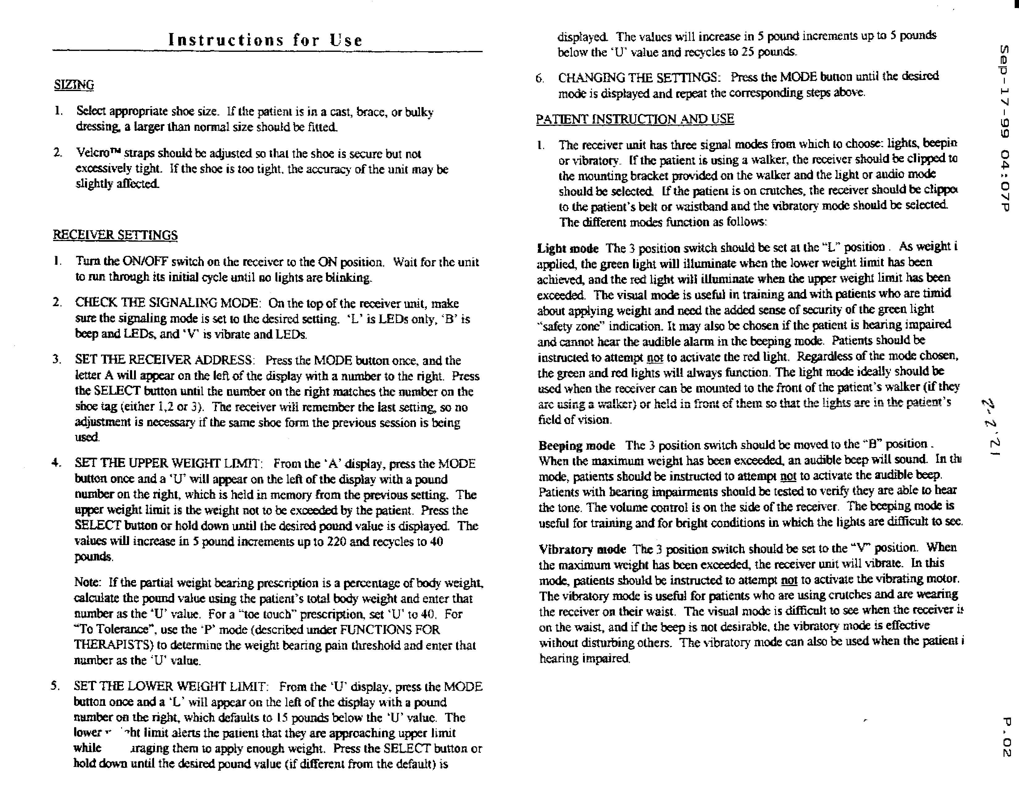
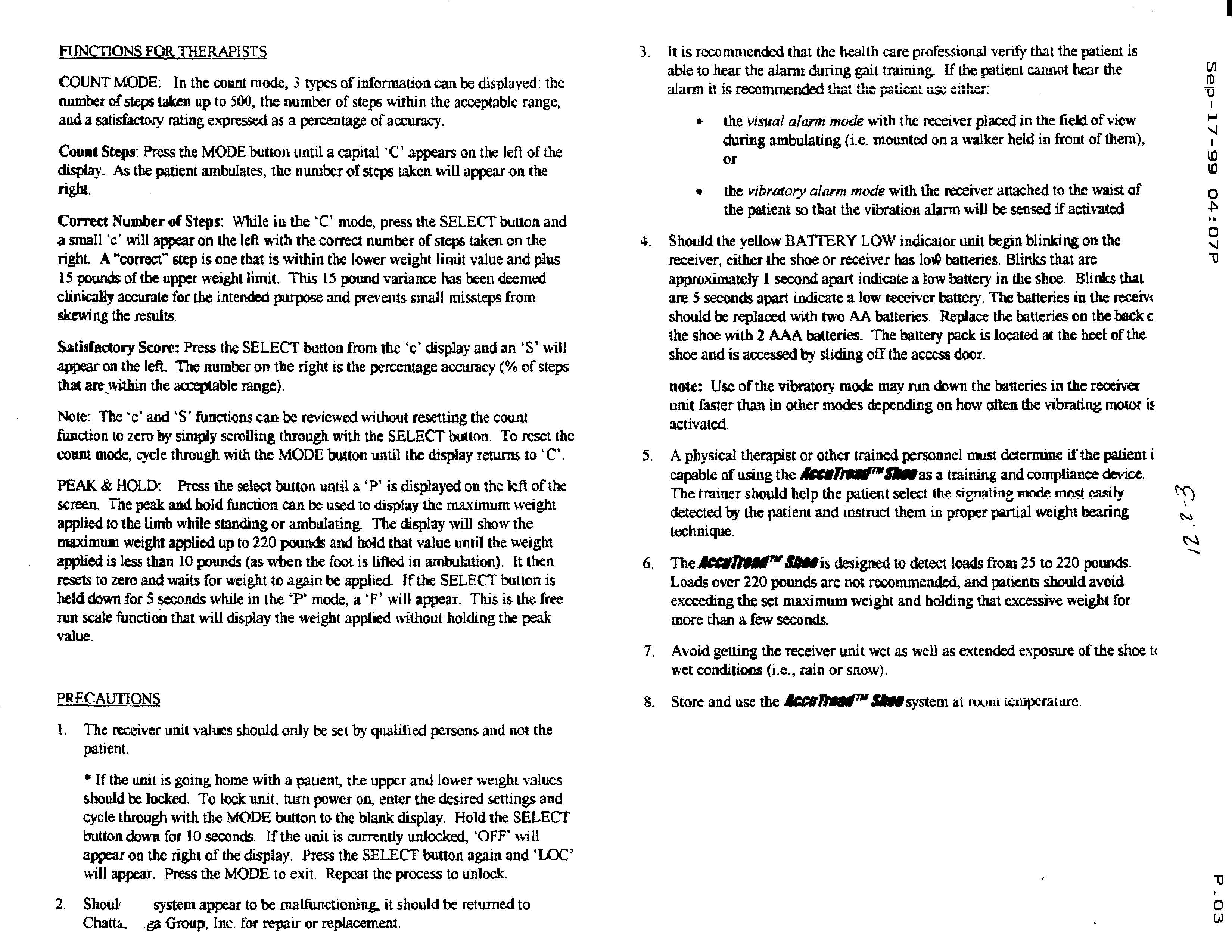
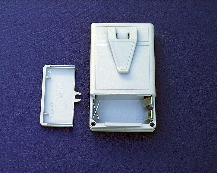
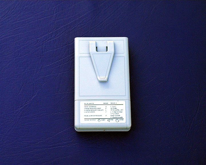
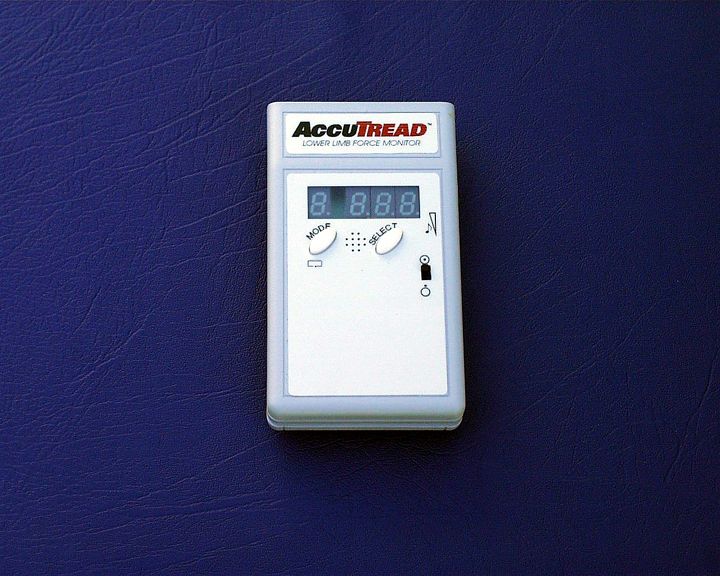
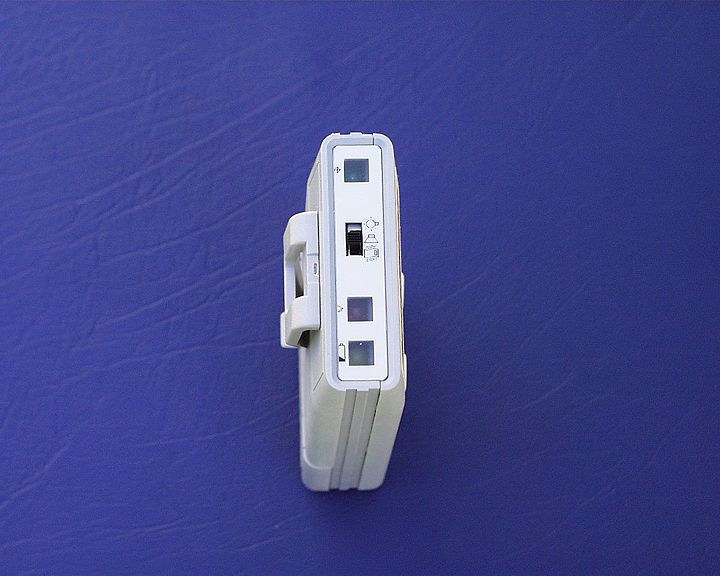
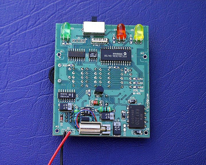
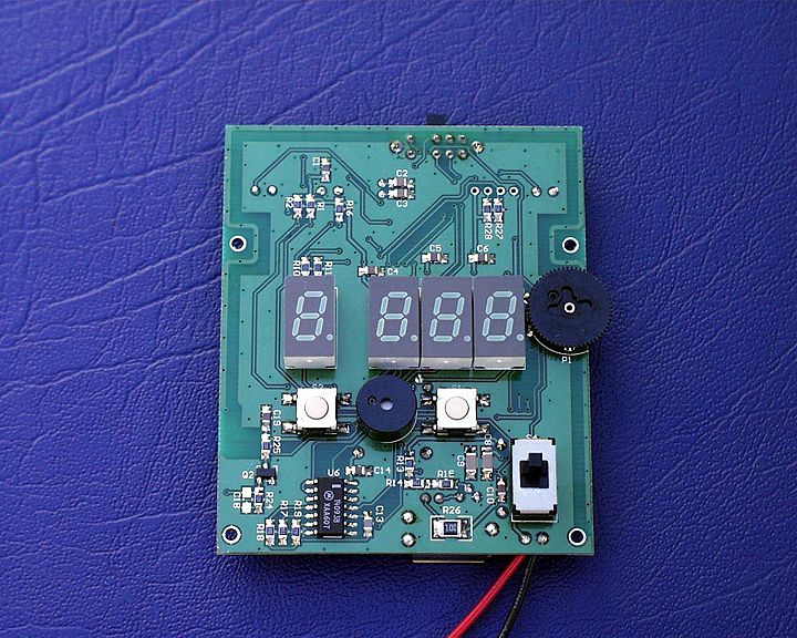
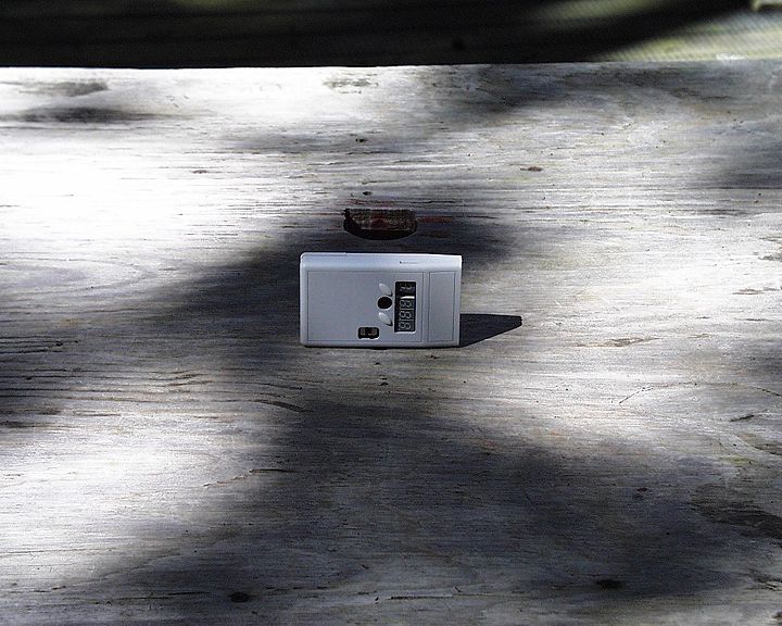
Description of Receiver Operation (Brief). The receiver electronics are part of a weight bearing shoe product that receives RF bursts of information at a rate of 20 per second. The receiver uses this information to display the weight on a numeric LED display, and in a variety of different sensory forms. The outputs make the patient aware of how much weight is being applied to their lower extremity. The output forms are LED’s for upper (Orange) and lower (Green) limits, and a blinking (Yellow) LED for low battery indications for both the transmitters and the receiver, a speaker with volume control for an audio alarm of the upper limit, and a vibrating motor for a sensory alarm of the upper limit. The LED display is used to view numeric values for weights, and to set the shoe address, upper and lower weight limits, and to use some calculation functions provided for patient rehabilitation. Moderately Detailed Circuit Description. Power is applied via a switch and in the form of 2x1.5 Volt AA batteries i.e. (a voltage that ranges from less than 1.6 to about 3.3 Volts). This in turn supplies a DC to DC converter, which generates a stable 3.3 Volts. This voltage then supplies power to the microcontroller, which then begins the start up process. It then collects data stored in memory in which it reads the user controlled shoe address, and the user controlled settings for upper and lower limit data. The program then goes into operation mode. The receiving chip constantly looks for a signal from one of the supplied shoe transmitters. The microcontroller receives a digital word that contains the shoe address, Hi/Lo battery indicating bit, the corrected 8 bit digital word for the weight, and error code correction. When a signal is received the microcontroller looks to see if the shoe address matches. If the shoe address is incorrect, the microcontroller disregards the rest of the information in that burst, and waits for another burst. When a signal has a matching address, the microcontroller accepts the data for interpretation. The microcontroller then compares the information with the onboard user preset values for upper and lower weight limits to send a signal to the different forms of alarms selected by the user. The yellow LED indicates low battery for both the receiver and transmitter. A slow blinking yellow LED indicates the transmitter battery is low and faster blinking yellow LED indicates the receiver battery is low. The green LED indicates the lower weight threshold has been exceeded. The orange LED indicates the upper weight threshold has been exceeded. The yellow, green, and orange LED’s are not user controlled in that they always will operate when the user set levels have been met. The user can control the threshold level of the green and orange LED’s, but that’s it. There are 4 forms of output: LEDS, Speaker, Vibrator, and LED display. A 3-way switch controls the LED’s, Speaker, and Vibrator. (Position 1) LED’s only (meaning green and orange LED’s), (Position 2) LED’s and speaker only, and (Position 3) LED’s and vibrator only. The speaker has a volume control knob for a low tone to high tone output. The LED display operates separately from the 3 settings of the 3-position switch. The LED display is controlled by 2 buttons one for the mode of display, and the second button to adjust the selected mode. The modes of operation are as follows, blank display, Shoe address, upper limit, lower limit, count mode, and peak and hold in that order. The mode button will cycle through this list again and again. The blank display mode saves battery power. Upper and lower limit modes can be adjusted in 5 Lbs. increments (upper ranges from 40 to 220 Lbs.) and (lower ranges from 25 to 215 Lbs.). The count mode counts the number of steps, the number of good steps, and displays the percentage of good steps over total steps. A correct step is determined between the lower limit and 15 Lbs. above the upper limit. The count mode can be cycled to the different output data formats by using the select button to go from count to the number of correct steps to the percentage of good steps and back again. The peak mode allows the user to view the amount of weight they loaded on the shoe in 1 Lbs. increments from 10 to 254 Lbs. The select button resets the mode to zero. Holding the button for 5 seconds will put the display in a mode of a free running scale. The peak mode will also reset and run another reading when the user steps down again. Pressing the mode button again will put the receiver back into the blank display mode. The display will also fall asleep after a few minutes of inactivity to save battery power, and then will wake up in the same place again as soon as it detects activity. The address, upper limit, and lower limit can be locked by pressing the select button for 5 seconds in the blank display mode, so the user can’t accidentally change the setting preset by the user. The product unit is to be sold as 3 size shoes, small, medium, and large i.e. (3 transmitters operating identically in the same fashion as described in the transmitter description only with a different shoe address for the different shoe sizes), and a receiver. In some instances it may be required of us to provide up to as many as 32 shoes/shoe addresses per receiver. The data transfer rate is 9600 baud with a burst duration of about 8.5 ms, 20 times per second at a carrier frequency of 418Mhz.
Schematics
123456 A B C D 654321 D C B A Title NumberRevisionSize B Date:18-Sep-1999Sheet of File:C:\FCCCERT\ACCURX3V.SCHDrawn By: Vcc Vcc Vcc Vcc Vcc Low Battery Out Low Battery In RS232 In RS232 Out uController Functions 1. 8-bit analog input 2. RS232 serial port to communicate with computer 3. ID Code input 5-bits 4. Output pulse to turn on power to the Load Cell 5. Low Battery input pin 6. Try to Design around a 3.3 Volt Vcc 7. 50 to 100 words transmitted per second OTR AccuShoe Receiver RX1 3A Rainer G. Riffert 2 of 5 Design Engineers: Rainer G. Riffert & Mike Blair P1 5K R3 100 R4 100 R5 100 R21 1K R25 100K R2 100K R1 100K SHDN 1 3/5 2 REF 3 LBO 4 LBI 5 OUT 6 GND 7 LX 8 U5 MAX856CSA D1 1N5817M L1 47uH + C7 47uF + C11 47uF D2 DL4148 C9 0.1uF C8 0.1uF R13 100K R14 330K 1 2 B1 2 x 1.5V R26 10 XTAL1 4.000MHz C2 18pF C3 18pF CS 1 CLK 2 DI 3 D0 4 GND 5 NC 6 NC 7 Vcc 8 U2 93C06 ANT1 ANTENNA C19 0.01uF C4 0.01uF MCLR*/Vpp 1 RA0 2 RA1 3 RA2 4 RA3 5 RA4/TOCKI 6 RA5/SS* 7 OSC1/CLKIN 9 OSC2/CLKOUT 10 RC0/T1OSO/T1CKI 11 RC1/T1OSI/CCP2 12 RC2/CCP1 13 Vss 8 Vss 19 RC3/SCK/SCL 14 RC4/SDI/SDA 15 RC5/SDO 16 RC6/TX/CK 17 RC7/RX/DT 18 RB0/INT 21 RB1 22 RB2 23 RB3 24 RB4 25 RB5 26 RB6 27 RB7 28 Vdd 20 U1 PIC16C63A 1 2 3 4 J1 CN4 Vcc D3 Green LED D4 Red LED D5 Yellow LED + - M1 Namiki Motor Q1 VN10LP S1 Select S2 Mode 2 1 4 7 8 5 3 6 9 10 Case S3 EG2315 Vcc + C15 10uf + C17 1uF Vcc A0 1 A1 2 A2 3 Latch Enable 4 CS2 5 CS1 6 GND 8 Y7 7 Y6 9 Y5 10 Y4 11 Y3 12 Y2 13 Vcc 16 Y1 14 Y0 15 U3 74HC237M R6 100 R7 100 R8 100 R9 100 R10 100 R11 100 R12 100 Vcc Vcc C6 0.01uF C1 0.01uF C5 0.01uF 1 A1 1 A2 1 A3 1 A4 R16 100K C10 0.01uF L2 47uH + C12 47uF ABC D E F G 123456 DP DP DIS1 4_SEG_DISPLAY Q2 VN10LF R20 2.2K S4 EG2209A R24 100K Motor Speaker Mode Select Green Red LB_Ind R15 100K IN1 1 IN2 2 IN3 3 IN4 4 IN5 5 IN6 6 IN7 7 GND 8 COM 9 OUT7 10 OUT6 11 OUT5 12 OUT4 13 OUT3 14 OUT2 15 OUT1 16 U4 MC1413B DATA OUT 7 +Vcc 1 GND 4 RF INPUT 10 Baseband Output 2 Comp Input 3 Theshold Override 5 Voltage Ref 6 GND 8 GND 9 U7 RX1320 + C16 10uf SP1 BUZZER1 Q3 2N3906 A R17 330K R18 100KR19 330K C13 1000pF C14 0.01uF In1A 1 In1B 2 Out1 3 Out2 4 In2A 5 In2B 6 VSS 7 In3A 8 In3B 9 Out3 10 Out4 11 In4A 12 In4B 13 VDD 14 U6 CD4093BE Vcc R27 100K R28 100K 1.628V Low Battery Threshold
Test Report
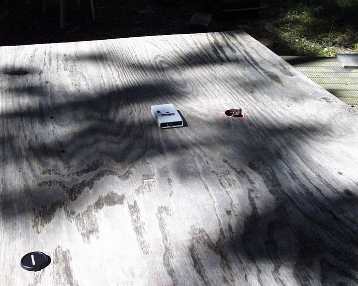
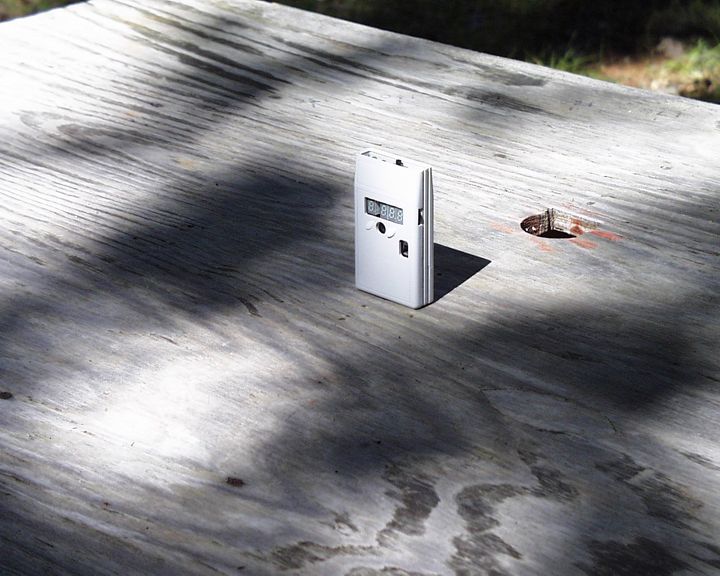
CD&T FCC ID: OP4ATS-RX418 A. DEVICE UNDER TEST The device is a low power data receiver used to receive and decode data transmissions from its companion transmitter (OP4ATS- TX418). The received data is translated into weight/force readings in pounds and appears on the receiver’s display. This product is designed to operate under the provisions of Part 15.109 of the FCC rules. The frequency of operation is 418 MHz. nominal. The device is powered by an internal battery supply consisting of two “AA” alkaline batteries. Testing was conducted with fresh batteries installed. During the test the batteries were checked periodically to insure that the optimum voltage range was maintained. This receiver of this device is a TRF circuit using SAW filters to achieve the desired receive frequency. A SAW delay line is employed to provide a time lag between two rf amplifiers so that the amplifiers may be alternately turned on and off (approx. 245kHz.) and thus realize a relatively high gain without instability. The entire receiver is contained in a single monolithic integrated circuit. The only external RF element is the antenna. There are no tunable elements in this device. B. MEASUREMENT PROCEDURE: RADIATED EMISSIONS Testing of this device and its associated transmitter (OP4ATS- TX418) was conducted at the Hyak Labs. Test facility in Spotsylvania, Virginia. Field strength measurements were conducted according to the procedures set forth in ANSI C63.4 (1992). The device was set to its normal mode of operation with a steady incoming data stream applied from its companion transmitter. The device under test was placed on a rotating turntable 0.8 meters high, centered at 3 meters distant from the measurement antenna. The device was placed in the center of the turntable and tested in the three logical positions shown in the test setup photographs. This device is designed to be hand held. In all positions, the primary source of emissions seemed to be in the plane parallel with the plane of the printed circuit board. The field strength measurements were taken using an HP8596E spectrum analyzer, an EMCO 3121C dipole set and an Avantek UJ210 preamp. The device was scanned from 30MHz. to 4.2GHz. and all emissions were noted. In this case the only emissions detected were those that were harmonically related to the microprocessor clock oscillator fundamental frequency. At each detected frequency, the device was measured by rotating the turntable and adjusting the antenna height over a range of 1 to 4 meters to obtain the maximum output level. This procedure was performed with both horizontal and vertical polarizations with the device in the positions described above. The peak reading for each frequency was recorded in the second column on the data sheet. No emissions were detected above 64 MHz.
Contact Information
Applicant
Frank B Gray(president)
(865) 588-3627Fax: (423) 585-2532
Technical Contact
Control Design and TestingThomas W Roche
[email protected](540) 582-2826
6010 Red Fox Drive · Spotsylvania, Virginia · United States
Technical Specifications
| # | Rule Parts | Frequency Range | Power Output |
|---|---|---|---|
| 1 | 15B | 417.6 MHz - 418.4 MHz | - |
Other Applications from Orthopedic Technology Research, Incorporated

OP4-ATS-TX418
Dec 14, 1999lower limb force monitoring device
Equipment Class
DSC - Part 15 Security/Remote Control Transmitter