OSPTRACSVehicle & Vessel Tracking Device
Racal NCS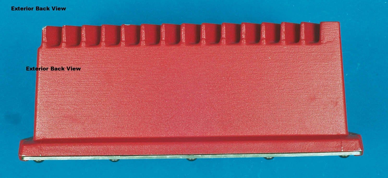
Click to zoom
Application Details
- Equipment Class
- TNB - Licensed Non-Broadcast Station Transmitter
- Date of Grant
- Feb 08, 2000
- Application Purpose
- Original Equipment
- Date of Application
- Nov 10, 1999
- Equipment Note
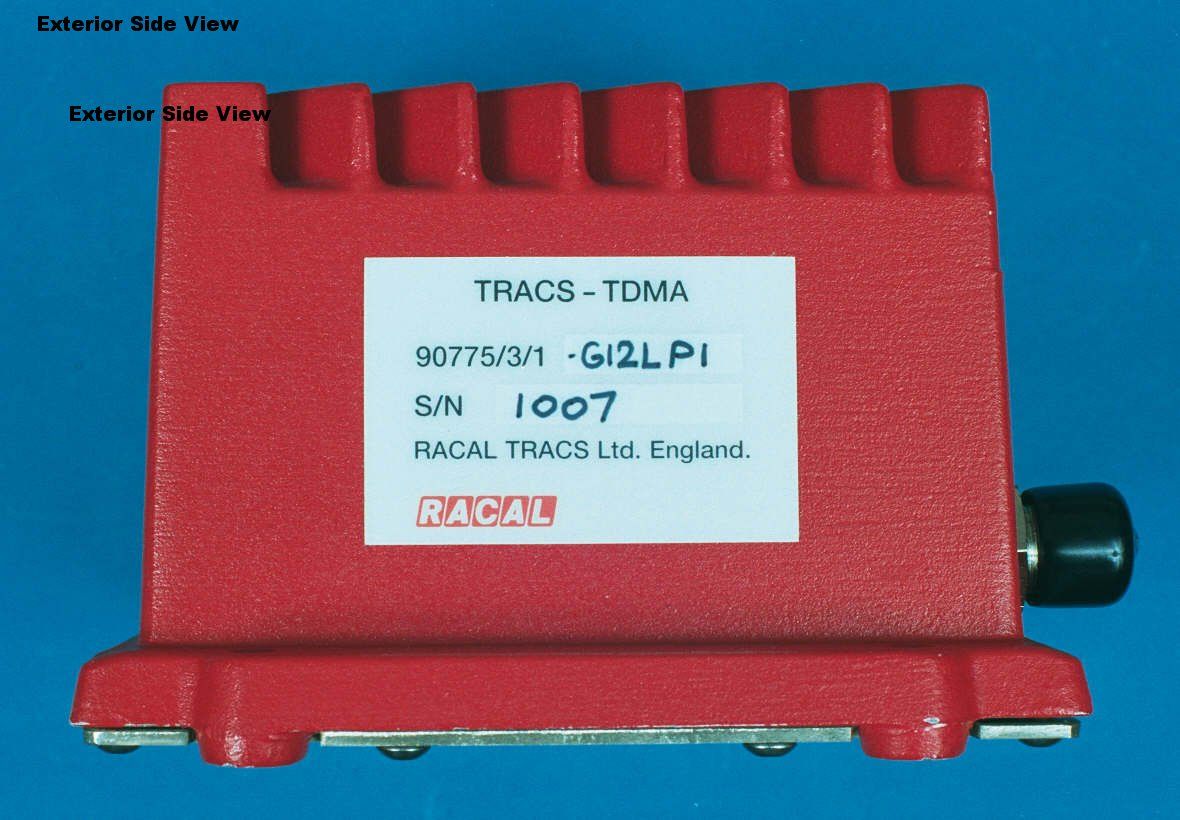
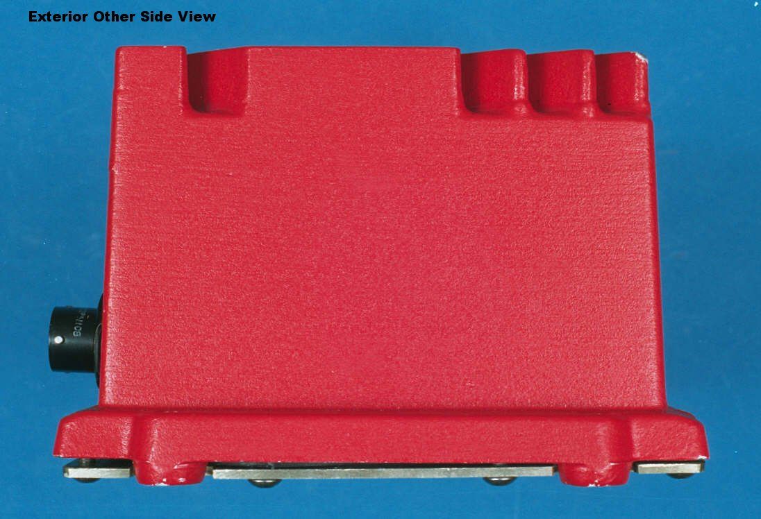
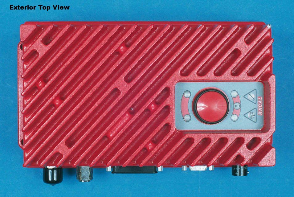
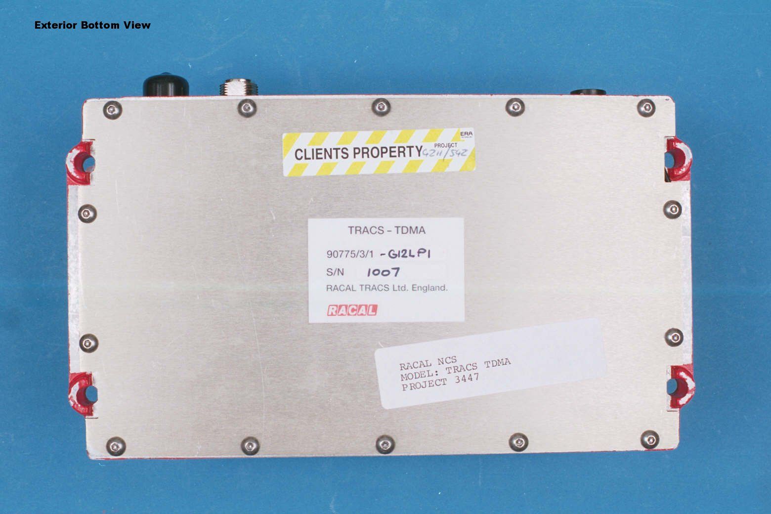
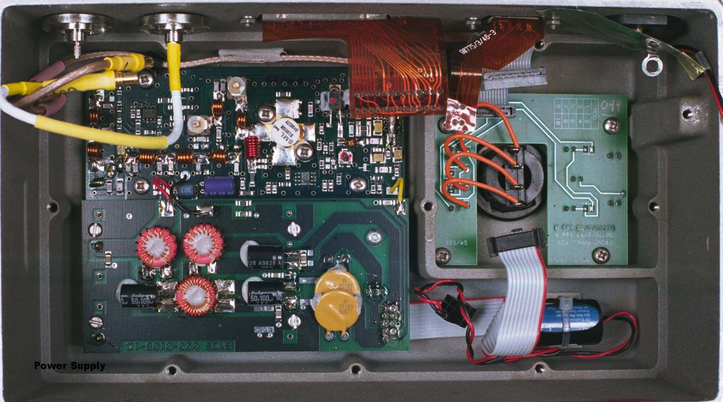
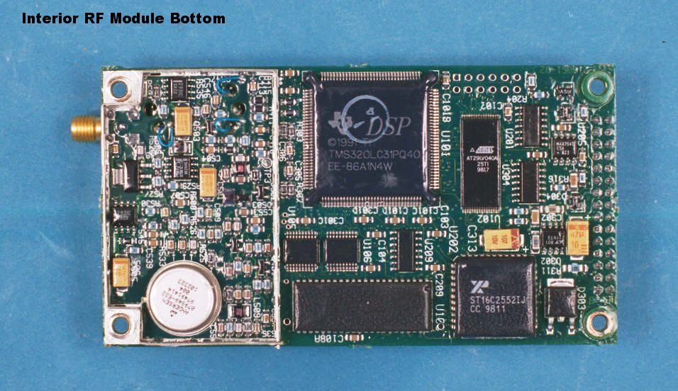
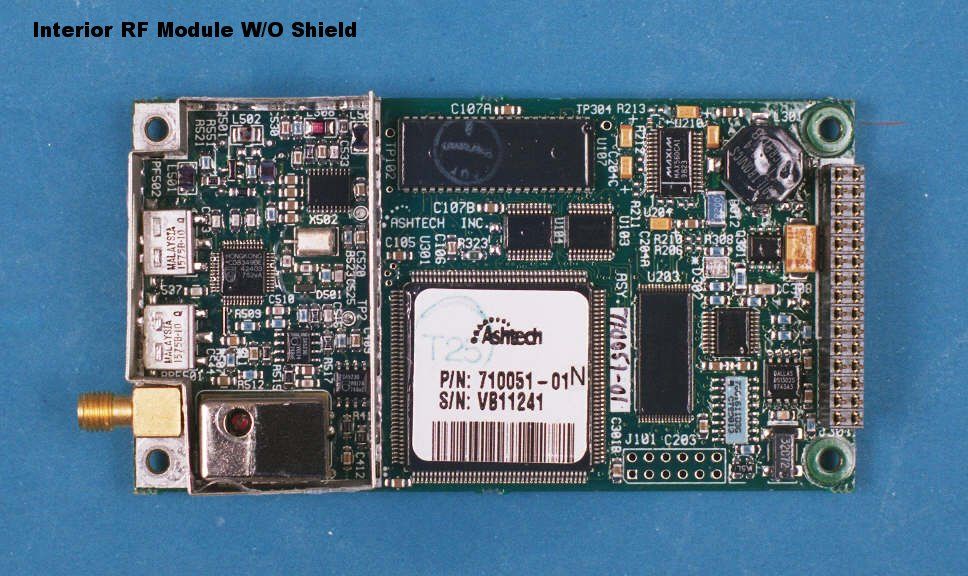
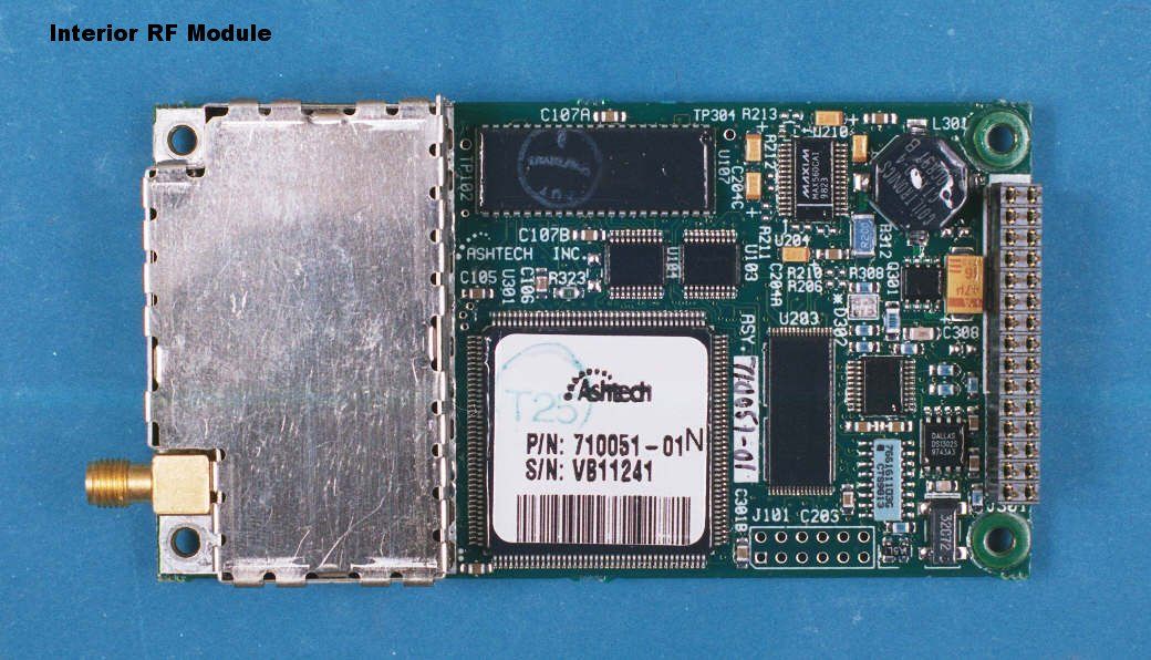
- Vehicle & Vessel Tracking Device
- Frequency Range
- 136.00000000 - 174.00000000
- Company
- Racal NCS
- Country
- United States
Documents & Files
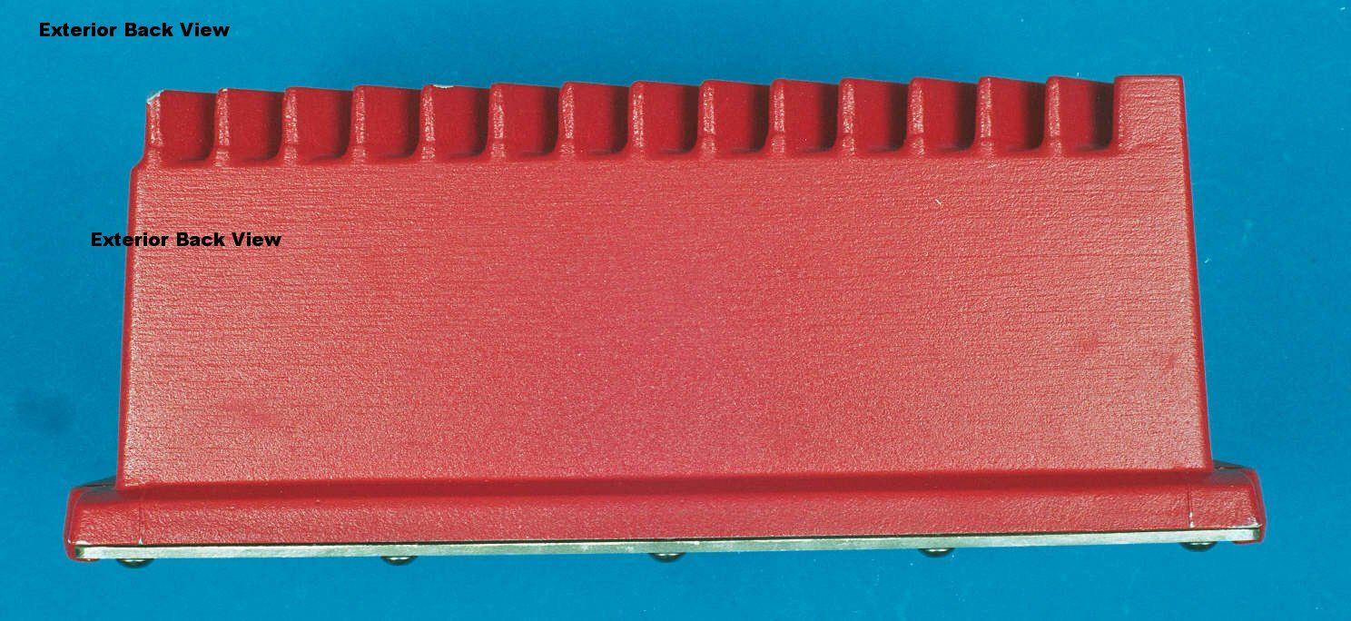
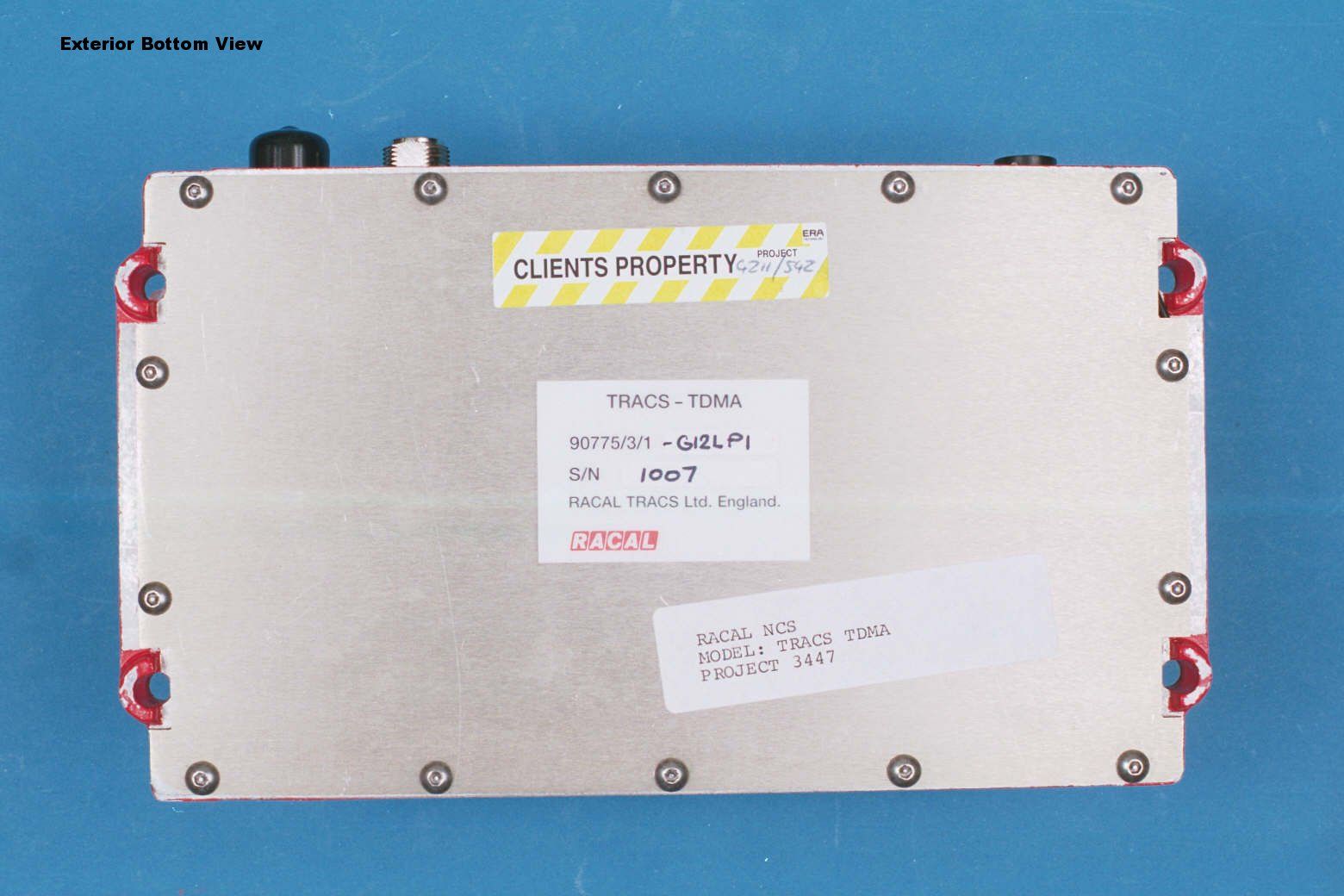
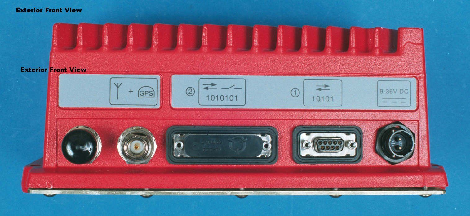
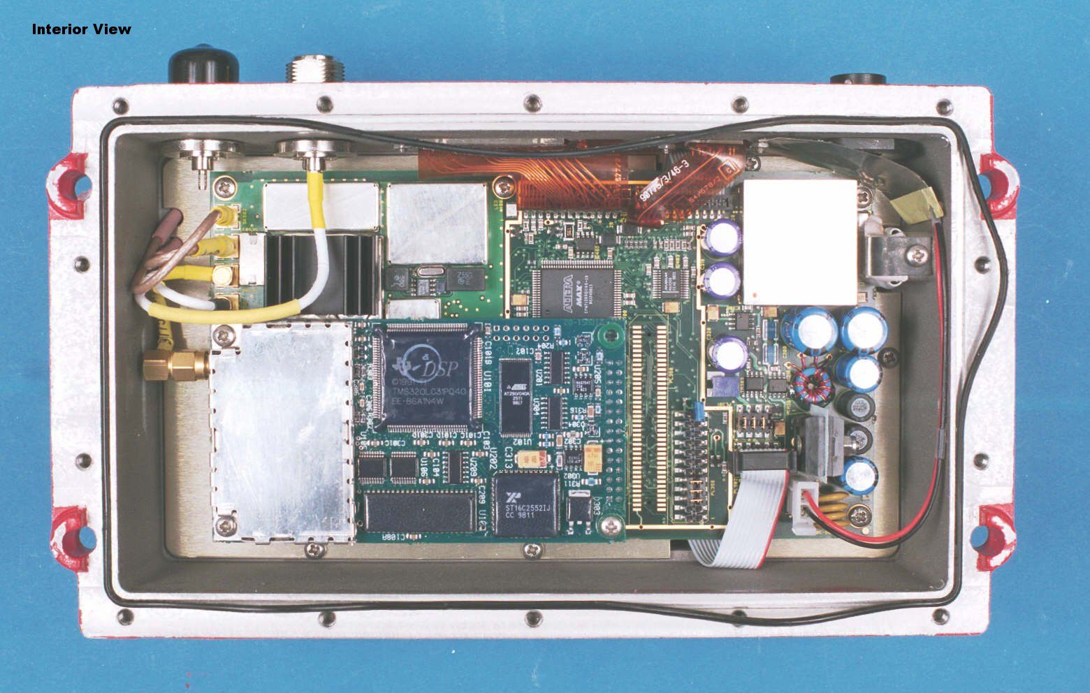
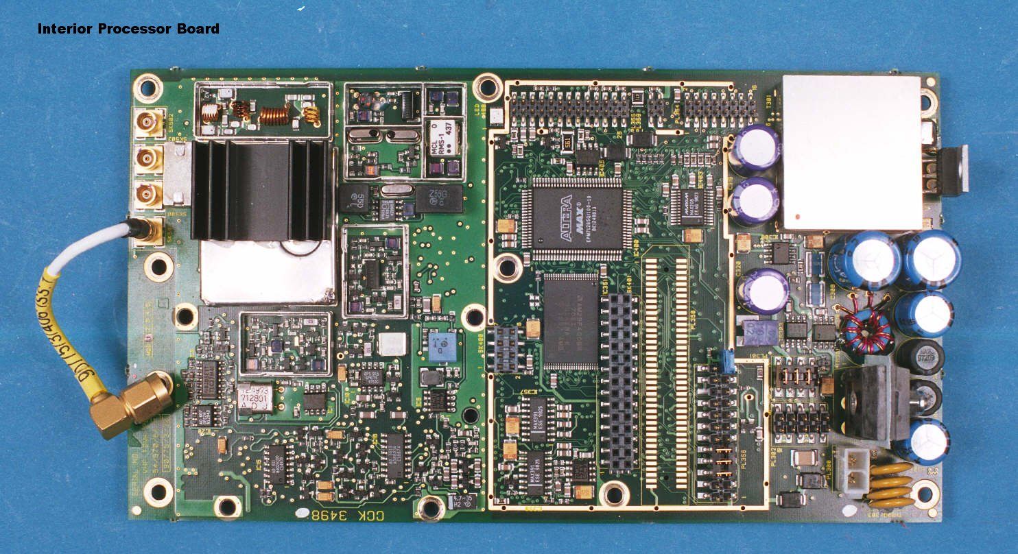
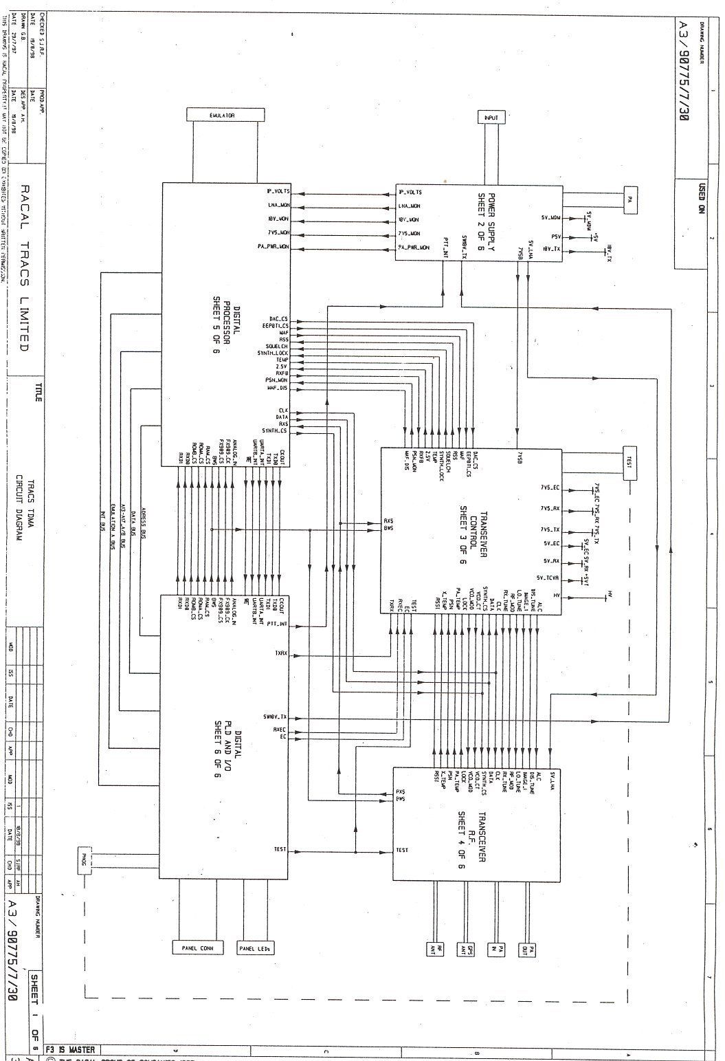
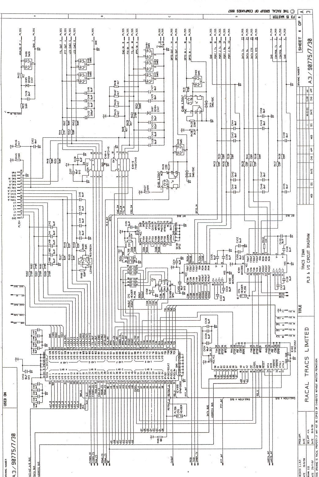
Document Text
Text extracted from the exhibit documents filed with the FCC. Open a document above to read the original.
Users Manual
c:\temp\hyak\Page0.gif c:\temp\hyak\Page1.gif c:\temp\hyak\Page2.gif c:\temp\hyak\Page3.gif c:\temp\hyak\Page4.gif c:\temp\hyak\Page5.gif c:\temp\hyak\Page6.gif c:\temp\hyak\Page7.gif c:\temp\hyak\Page8.gif c:\temp\hyak\Page9.gif c:\temp\hyak\Page10.gif c:\temp\hyak\Page11.gif c:\temp\hyak\Page12.gif c:\temp\hyak\Page13.gif c:\temp\hyak\Page14.gif c:\temp\hyak\Page15.gif c:\temp\hyak\Page16.gif c:\temp\hyak\Page17.gif c:\temp\hyak\Page18.gif c:\temp\hyak\Page19.gif c:\temp\hyak\Page20.gif c:\temp\hyak\Page21.gif c:\temp\hyak\Page22.gif c:\temp\hyak\Page23.gif c:\temp\hyak\Page24.gif c:\temp\hyak\Page25.gif c:\temp\hyak\Page26.gif c:\temp\hyak\Page27.gif c:\temp\hyak\Page28.gif c:\temp\hyak\Page29.gif c:\temp\hyak\Page30.gif c:\temp\hyak\Page31.gif c:\temp\hyak\Page32.gif c:\temp\hyak\Page33.gif c:\temp\hyak\Page34.gif c:\temp\hyak\Page35.gif c:\temp\hyak\Page36.gif c:\temp\hyak\Page37.gif c:\temp\hyak\Page38.gif c:\temp\hyak\Page39.gif c:\temp\hyak\Page40.gif c:\temp\hyak\Page41.gif c:\temp\hyak\Page42.gif c:\temp\hyak\Page43.gif c:\temp\hyak\Page44.gif c:\temp\hyak\Page45.gif c:\temp\hyak\Page46.gif c:\temp\hyak\Page47.gif c:\temp\hyak\Page48.gif c:\temp\hyak\Page49.gif
Operational Description
ALIGNMENT PROCEDURE Test No. Parameter Stimulus Monitor Limit Notes 01.01 5 Volt Current From a 500mA current limited supply, apply 5 volts DC toPL301/4 wrt PL301/2 5v Input current 10mA to 400mA Input Voltage into PL300 and 7.5 and 10 volts for the radio not required until later.Record value 02.01 PLD Configuration Select the ' Max Plus 2 - Programming' menu item. Select the program option Package response, Sat/UnsatVerification of theprogramming process.Examine, Programme, andVerify OK Using the Altera Max + Plus II programming softwarepackage.Choose the PLD program configuration file (.POF)specified in configuration document.Connect the PC to the PLD JTAG interface port via thePL351 connector. 03.01 Processor Initialise Connect bootload link across PL356/3 to PL356/4. Apply inputpower. Reset processor usingPL356/2 pulled to groundPL356/1 then disconnected.From the PC send a Null character(00H) as per 90775/18/310 The RS232 transmit line.PL359/2. Sat/UnsatRS232 response : Returnof a single ‘U’ character(55H) Connect Control Serial port to Processor input port ViaPL359/1 0v, PL359/2 Tx, PL359/3 Rx. 03.01.01 Processor Initialiseresponse failed As above. PL356/18 command_rx_ttl PL356/17 command_tx_ttl Sat/UnsatRS232 TTL response Look for fail either side of MAX208 or in processor 03.01.02 Processor Initialiseresponse still fails 5v Power only XTAL1 PL350/40 18.432Mhz signal Now probing by hand using > 40MHz oscilloscope. 03.02 Load preload32 program From the PC send the preload32 program as per 90775/18/310PL359/3 control Rx The RS232 transmit line.PL359/2 Sat/UnsatRS232 response : Returnof a single ‘P’ character This test is part of a continues no power breaksequence. 03.03 Load Processor Xram test Send ram test program. Drive as per 90775/18/310PL359/3 control Rx The RS232 transmit line.PL359/2 Sat/Unsat Tests Ram from within Processor prior to loading Ram to test Flash. 03.03.01 Load Processor port test -Xram fail Follow from load preload32program. Send port test program.Drive as per 90775/18/310PL359/3 control Rx The RS232 transmit line.PL359/2 Sat/Unsat 2 stage process setting direction and reading values Test No. Parameter Stimulus Monitor Limit Notes 04.01 Download Flash Test Follow from load preload32 program Send Flash Test program.Drive as per 90775/18/310 The RS232 transmit line.PL359/2 Sat/Unsat 04.02 Software Identification PL359/3 control Rx Drive as per 90775/18/310 The RS232 transmit line.PL359/2 Sat/Unsat 04.03 Flash A sector test PL359/3 control Rx Drive as per 90775/18/310 The RS232 transmit line.PL359/2 Sat/Unsat 04.04 Flash B sector test PL359/3 control Rx Drive as per 90775/18/310 The RS232 transmit line.PL359/2 Sat/Unsat 04.05 Store Ftest Results PL359/3 control Rx Drive as per 90775/18/310 The RS232 transmit line.PL359/2 Sat/Unsat 04.06 Set Serial Number PL359/3 control Rx Drive as per 90775/18/310 The RS232 transmit line.PL359/2 Sat/Unsat 04.07 Download Downloader PL359/3 control Rx Drive as per 90775/18/310 The RS232 transmit line.PL359/2 Sat/Unsat 04:08 Software identification PL359/3 control Rx Drive as per 90775/18/310 The RS232 transmit line.PL359/2 Sat/Unsat 04.09 Check Boot code area PL359/3 control Rx Drive as per 90775/18/310 The RS232 transmit line.PL359/2 Sat/Unsat 04.10 Load Boot Code PL359/3 control Rx Drive as per 90775/18/310 The RS232 transmit line.PL359/2 Sat/Unsat 04.11 Copy Boot Code PL359/3 control Rx Drive as per 90775/18/310 The RS232 transmit line.PL359/2 Sat/Unsat 04.12 Load Loader Code PL359/3 control Rx Drive as per 90775/18/310 The RS232 transmit line.PL359/2 Sat/Unsat 04.13 Load ATE code PL359/3 control Rx Drive as per 90775/18/310 The RS232 transmit line.PL359/2 Sat/Unsat 04:14 Software Identification PL359/3 control Rx Drive as per 90775/18/310 The RS232 transmit line.PL359/2 Sat/Unsat 05.01 LED red test Drive RED as per 90775/18/310, PL359/3 control Rx Optically check Led400Red. Sat/Unsat User input required 05.02 LED green test Drive GREEN as per 90775/18/310 PL359/3 control Rx Optically check Led400Green Sat/Unsat User input required Test No. Parameter Stimulus Monitor Limit Notes 05.03 Display output drive L1 Drive PL354/9 high. Drive as per 90775/18/310 All PL354 outputs 3,4,6,7,8,9,10,11,12,13,14,16 Sat/Unsat Only PL354/9 high Drive the other outputs low. The PWR output shouldalways be high. All outputs tied to 0v via resistor. 05.04 Display output drive L2 Drive PL354/13 high. Drive as per 90775/18/310 All PL354 outputs 3,4,6,7,8,9,10,11,12,13,14,16 Sat/UnsatOnly PL354/13 high. Drive the other outputs low. The PWR output shouldalways be high. All outputs tied to 0v via resistor. 05.05 Display output drive L3 Drive PL354/11 high. Drive as per 90775/18/310 All PL354 outputs 3,4,6,7,8,9,10,11,12,13,14,16 Sat/UnsatOnly PL354/11 high. Drive the other outputs low. The PWR output shouldalways be high. All outputs tied to 0v via resistor. 05.06 Display output drive L4 Drive PL354/12 high. Drive as per 90775/18/310 All PL354 outputs 3,4,6,7,8,9,10,11,12,13,14,16 Sat/UnsatOnly PL354/12 high. Drive the other outputs low. The PWR output shouldalways be high. All outputs tied to 0v via resistor. 05.07 Display output drive L5 Drive PL354/14 high. Drive as per 90775/18/310 All PL354 outputs 3,4,6,7,8,9,10,11,12,13,14,16 Sat/UnsatOnly PL354/14 high. Drive the other outputs low. The PWR output shouldalways be high. All outputs tied to 0v via resistor. 05.08 Display output drive TXRX_G Drive PL354/10 high.Drive as per 90775/18/310 All PL354 outputs 3,4,6,7,8,9,10,11,12,13,14,16 Sat/UnsatOnly PL354/10 high. Drive the other outputs low. The PWR output shouldalways be high. All outputs tied to 0v via resistor. 05.09 Display output drive TXRX_R Drive PL354/8 high.Drive as per 90775/18/310 All PL354 outputs 3,4,6,7,8,9,10,11,12,13,14,16 Sat/UnsatOnly PL354/8 high. Drive the other outputs low. The PWR output shouldalways be high. All outputs tied to 0v via resistor. 05.10 Display output drive STAT-G Drive PL354/7 high.Drive as per 90775/18/310 All PL3…
Text truncated - open the document above for the full version.
Test Report
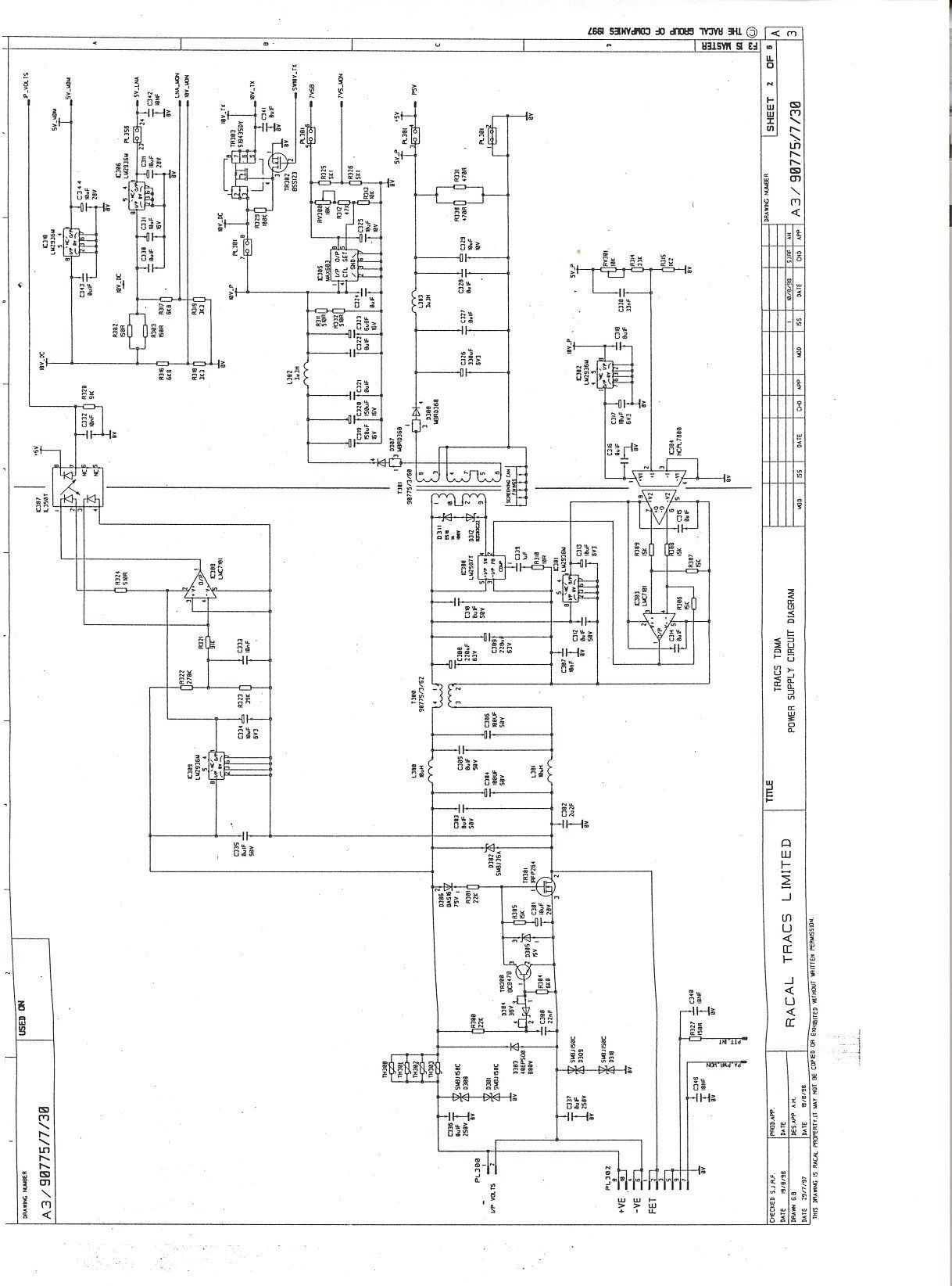
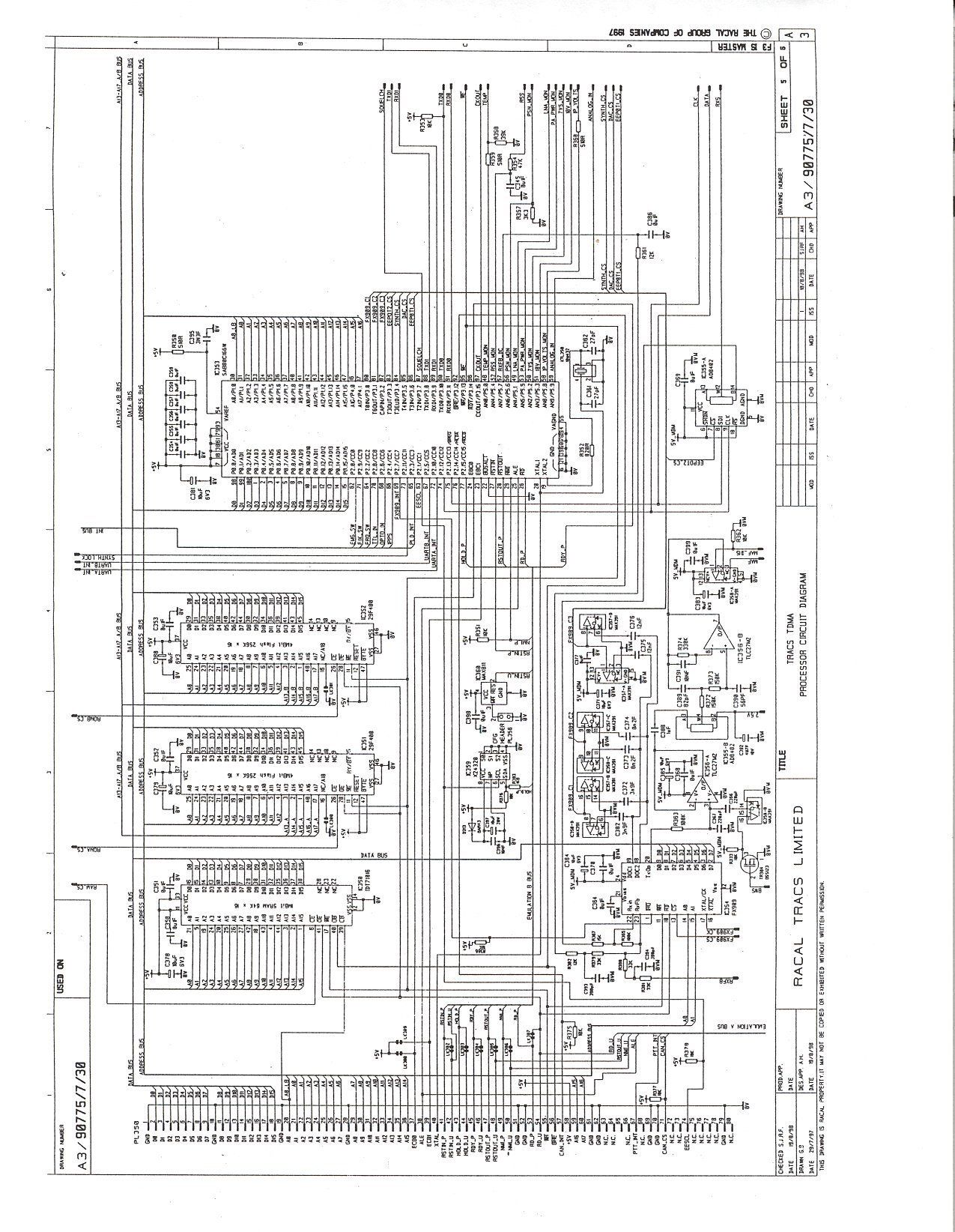
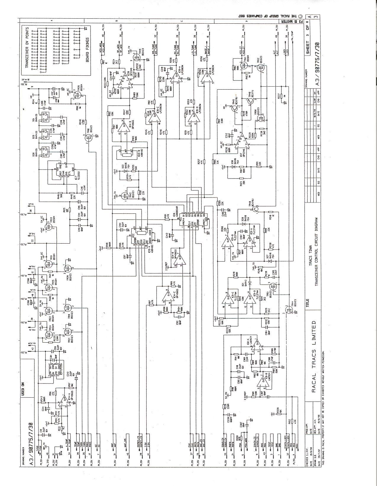
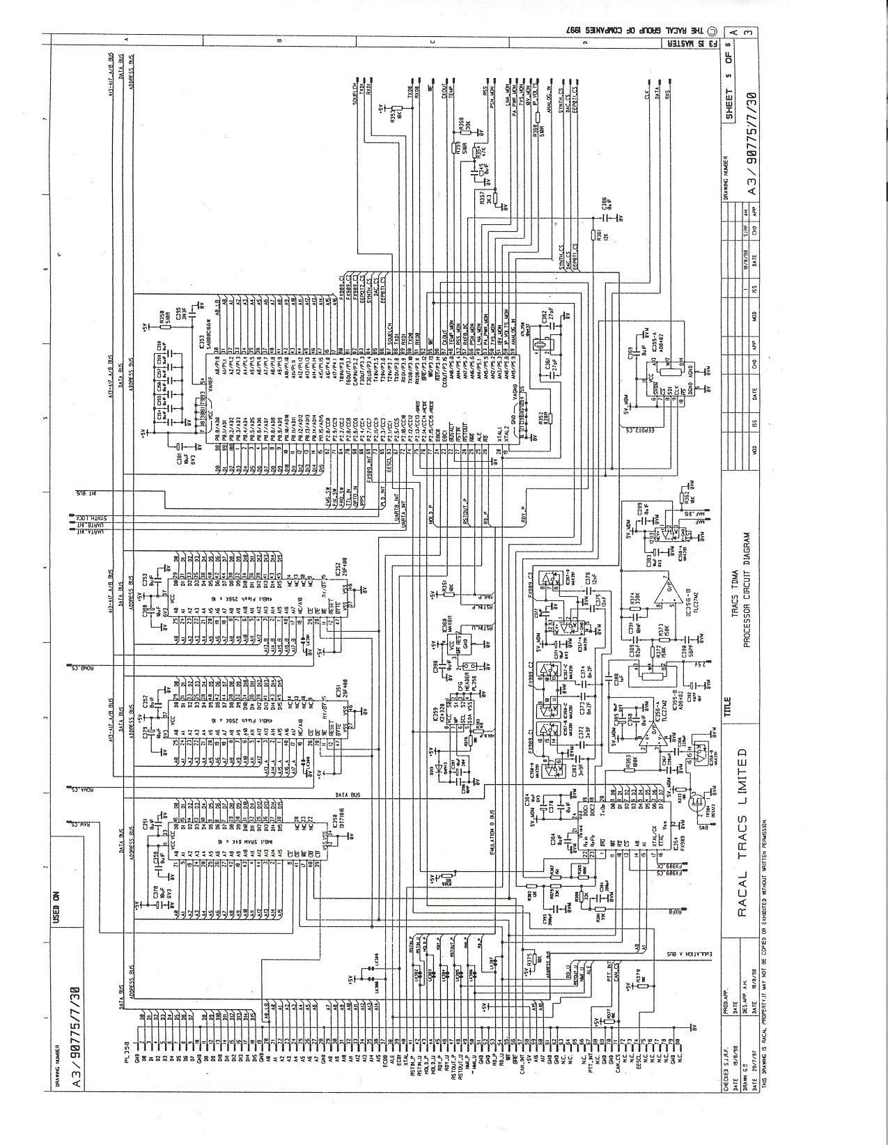
ENGINEERING STATEMENT For Type Certification of Racal NCS, Inc. Model No. Tracs TDMA FCC ID: OSPTRACS I am an Electronics Engineer, a principal in the firm of Hyak Laboratories, Inc., Springfield, Virginia. My education and experience are a matter of record with the Federal Communications Commission. Hyak Laboratories, Inc. has been authorized by Racal NCS, Inc., to make type certification measurements on the Tracs TDMA transceiver. These tests made by me or under my supervision in our Springfield laboratory. Test data and documentation required by the FCC for type certification are included in this report. The data verifies that the above mentioned transceiver meets FCC requirements and type certification is requested. _________________________ Rowland S. Johnson Dated: October 12, 1999 A. INTRODUCTION The following data are submitted in connection with this request for type certification of the Tracs TDMA transceiver in accordance with Part 2, Subpart J of the FCC Rules. The Tracs TDMA is a VHF, non-voice, 25/12.5 kHz channel, 10 watt transceiver intended for data-link applications in the 136-174 MHz band, operating under Subpart D, Industrial Radio Services, using time division multiple access, (TDMA) Gaussian minimum shift keying (GMSK). Tracs TDMA is a high speed, intelligent network radio datalink which operates in the VHF/UHF band to provide an addressable network datalink with integrated position reporting from an internal or external GPS receiver. It is primarily intended for vehicle and vessel tracking applications although it can be used for general data communication. B. GENERAL INFORMATION REQUIRED FOR TYPE CERTIFICATION (Paragraph 2.983 of the Rules) 1. Name of applicant: Racal NCS, Inc. 2. Identification of equipment: FCC ID: OSPTRACS a. The equipment identification label is submitted as a separate exhibit. b. Photographs of the equipment are submitted as a separate exhibit. 3. Quantity production is planned. 4. Technical description: a. 16k9F1D or 11k1F1D emission b. Frequency range: 136 - 174 MHz c. Operating power of transmitter is fixed at the factory at 10 watts, and can be Programmed to 500 mW. d. Maximum power permitted under Part 90 of the FCC is 350 watts, and the Tracs TDMA fully complied with those power limitations. e. The dc voltage and dc currents at final amplifier: Collector voltage: 10.0 V Collector current: 1.9 mA f. Function of each active semiconductor device: See Appendix 1. g. Circuit diagrams (6) are submitted as a separate exhibit. h. User instruction book is submitted as a separate exhibit. i. Transmitter tune-up procedure is submitted as a separate exhibit. j. A description of circuits for stabilizing frequency. See Appendix 3. 2 B. GENERAL INFORMATION...(Continued) k. A description of circuits and devices employed for suppression of spurious radiation And for limiting modulation. See Exhibit 4. l. Not applicable. 5. Data for 2.985 through 2.997 follow this section. 6. Transient frequency behavior of the equipment is included in Appendix 2. 7. RF Power Output (Paragraph 2.985(a) of the Rules) RF power output was measured with a Bird 4421 RF power meter and a Narda 765-20 attenuator as a 50 ohm dummy load. Maximum power measured was 9.8W, minimum 0.5W. The transmitter was tuned according to the procedure of Exhibit 4 with a supply voltage of 13.8 Vdc. C. MODULATION CHARACTERISTICS 1. The Tracs TDMA has no provisions for voice input and is intended only for data transmission. The requirements 2.987(a)(b), 90.211(c) and 90.211(d) do not apply. 2. Occupied Bandwidth (Paragraphs 2.989(c) and 90.209(c) or (d) of the Rules) Figures 1a and 1b; 2a and 2b are plots of the sideband envelope of the transmitter for both 25 and 12.5 kHz channels at rated Hi/Lo power level, taken from a Advantest R3361A spectrum analyzer. CW reference level was 0 dBm (top of screen) for each plot, with modulation corresponding to 19.2/9.6 kps channel efficiency respectively per 90.203(j)(3), and consisted of internally generated random data. The plots are within the limits imposed by Paragraph 90.209(c)/90.209(d) for frequency modulation. The horizontal scale (frequency) is 10 kHz per division and the vertical scale (amplitude) is a logarithmic presentation equal to 10 dB per division. Resolution bandwidth was 100 Hz; video bandwidth was 100 kHz. Emission designator was determined by measurement of the spectrum occupied by 99% of the emitted power, using an HP 8569E spectrum analyzer. 3 FIGURE 1a OCCUPIED BANDWIDTH 25 kHz, 10 watt ATTENUATION IN dB Required (1) On any frequency of more than 5 kHz but less than 10 kHz: At least 83 Log 10 (fd/5) decibels. 25 (2) On any frequency of more than 10 kHz up to and including 250% (50 kHz) of the authorized 20 kHz bandwidth: At least 29 Log 10 (fd 2 /11) 50 decibels or 50 decibels, whichever is the lesser attenuation. (3) On any frequency removed from the assigned frequency by 43+10 LogP = 53 more than 250% of the authorized (P = 9.8W) bandwidth (over 50 kHz). 4 FIGURE 1b OCCUPIED BANDWIDTH 25 kHz, 0.5 watt ATTENUATION IN dB Required (1) On any frequency of more than 5 kHz but less than 10 kHz: At least 83 Log 10 (fd/5) decibels. 25 (2) On any frequency of more than 10 kHz up to and including 250% (50 kHz) of the authorized 20 kHz bandwidth: At least 29 Log 10 (fd 2 /11) 50 decibels or 50 decibels, whichever is the lesser attenuation. (3) On any frequency removed from the assigned frequency by 43+10 LogP = 40 more than 250% of the authorized (P = 0.5W) bandwidth (over 50 kHz). 5 FIGURE 2a OCCUPIED BANDWIDTH 12.5 kHz, 10 watt ATTENUATION IN dB Required (1) On any frequency from the center of the authorized bandwidth f o to 5.625 kHz removed from f o : Zero dB 0 (2) On any displacement frequency of more than 5.625 kHz but no more than 12.5 kHz: At least 7.27(f d – 2.88 kHz) dB. 70 (3) On any displacement frequency of more than 12.5 kHz: At least 50 + 10 log (P) dB or 70 dB, whichever is the lesser attenuation. 50+10 LogP = 60 (P = 9.8W) 6 F…
Text truncated - open the document above for the full version.
Contact Information
Applicant
Angela Mejia(Legal Officer)
[email protected](713) 784-4482
Technical Contact
Hyak Laboratories, Inc.Rowland S Johnson
[email protected](703) 451-1188
7011 Calamo St., Suite 107 · Springfield, Virginia · United States
Non-Technical Contact
Hyak Laboratories, Inc.Georgia Hall
[email protected](703) 451-1188
Technical Specifications
| # | Rule Parts | Frequency Range | Power Output | Emission | Tolerance |
|---|---|---|---|---|---|
| 2 | 90.21 | 136 MHz - 174 MHz | 10 W | 11K1F1D | 0.00025 % |