OVWXH9-RXReceiver for water timer
Bondrich Development Limited
Click to zoom
Application Details
- Equipment Class
- CYY - Communications Receiver used w/Pt 15 Transmitter
- Date of Grant
- Apr 09, 2001
- Application Purpose
- Original Equipment
- Date of Application
- Apr 09, 2001
- Equipment Note
- Receiver for water timer
- Frequency Range
- 315.00000000 - 315.00000000
- Company
- Bondrich Development Limited
- Country
- Hong Kong
Documents & Files
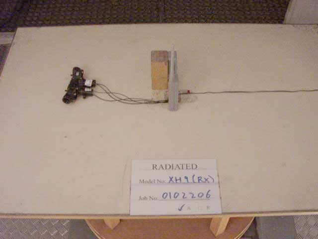
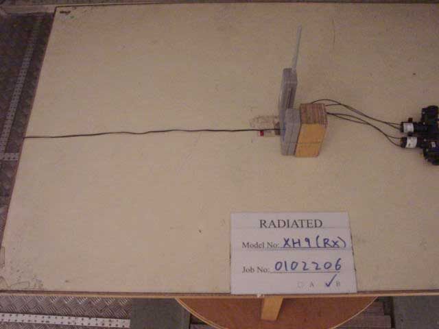
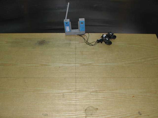
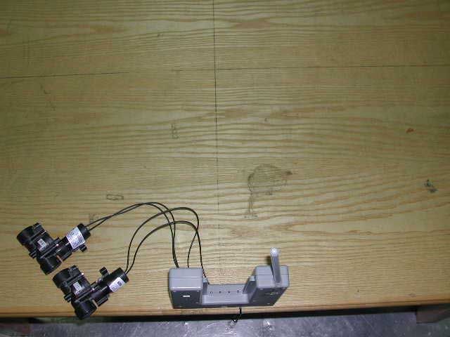
Document Text
Text extracted from the exhibit documents filed with the FCC. Open a document above to read the original.
Operational Description
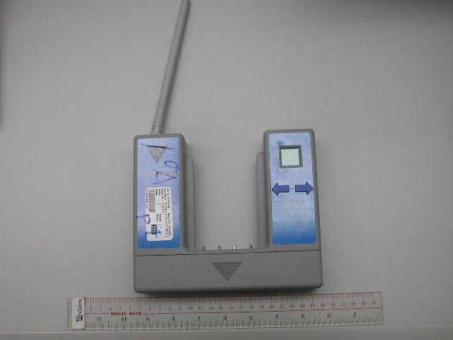
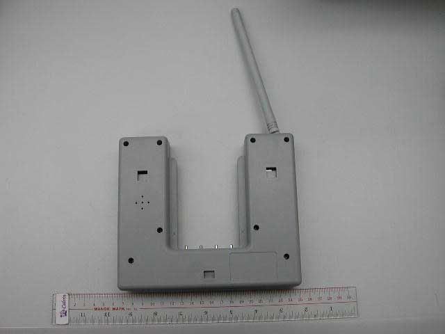
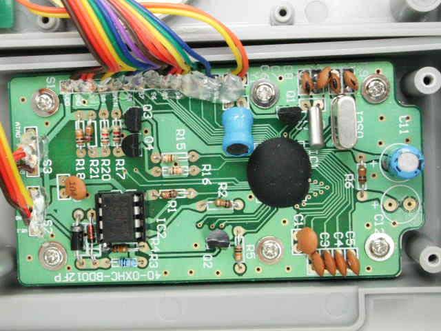
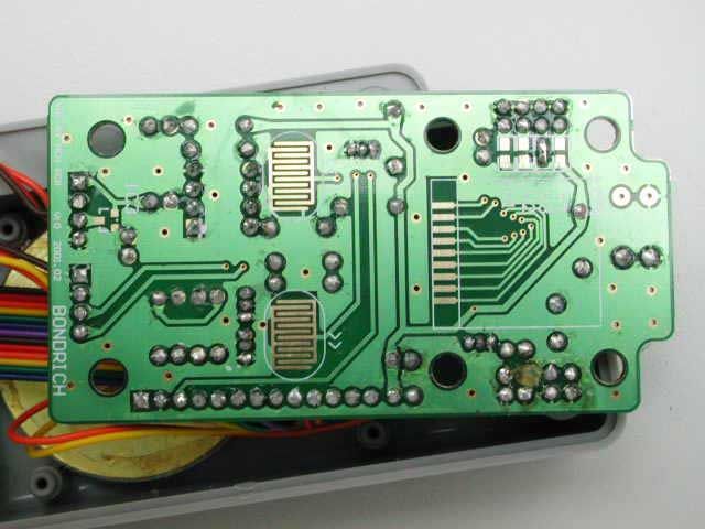
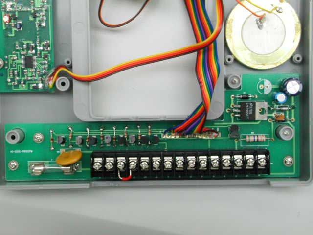
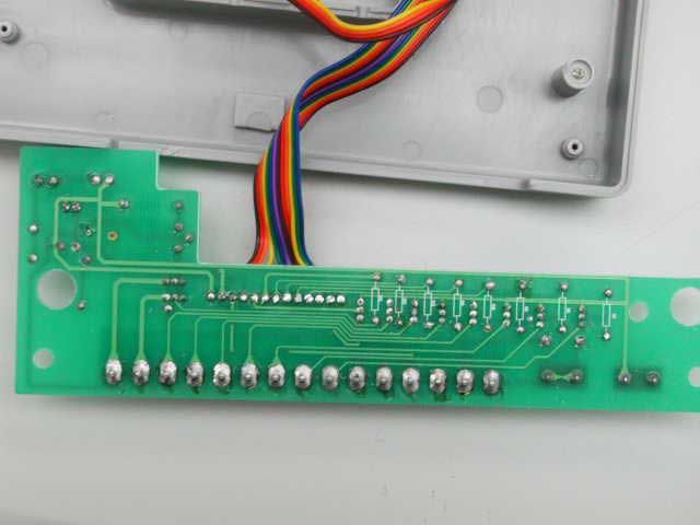
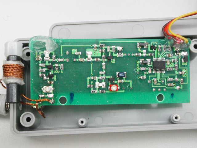
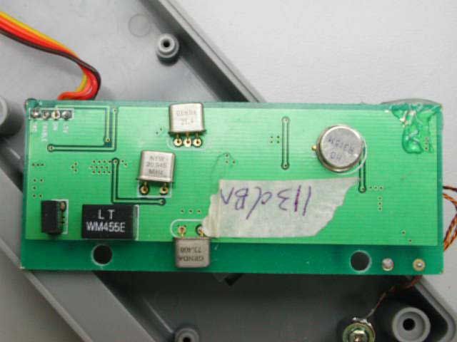
Main Structure of Rx unit The Rx Unit (Base Unit), the mainly RF received communication channel is 315MHz, the structure of the Rx unit include 8 bit MCU, 16k EEPROM, 315MHz RF Receiver board, LCD display, keypad input, Control Solenoid output & 4pins marry communication channel with base unit. The supply source by 24V AC. RF Board The Receiver RF board, the fundamental oscillator frequency is 73.4MHz and the data received Base received sensitivity is “- 60dBuV”. On the circuit U1 TA1142FN function is demodulation the incoming signal. The Q3 “2SC3585” is the local oscillator & Q5 “2SC3585” transistor are the side band frequency filter, signal voltage regulator & Mixer signal to IC. The IF frequency is 455KHz by the U2 Ceramic Discriminator. MCU The 8 bit MCU (HE89A22) is main control in the TX unit, This is received the RF board data, control External Memory (16K EEPROM), LCD display & Solenoid on/off. The main duty of MCU is represent the state from input ports (Key Pad or Low battery detected) and display the program states on the LCD display & output control on the Solenoid. The MCU can store the program data in to the external memory “EEPROM”. The function of the C1, C2, C3, C4 & C5 is LCD Charge Pump setting, IC3 16K EEPROM function is the external memory in the circuit OSC1 is 4MHz for Fast Clock of internal interrupt Program. OSC2 is 32768Hz for slow Clock & Real Time Clock of Program. This is the External memory for automatic store the program data, when change the dial key position. I/O Port 3 Group of input port in the Rx unit; a/ Key pads input. b/ Output pins Control for Solenoids. c/ Received Data Decode. d/ Data information port (for EEPROM & for Marry operation) e/ Rain Sensor Marry Operation When let TX Unit & Base Unit has connected together, the 4 pins connection pins have created the communication channel for transfer the “date / time / Base number / Security Code” from Base Unit to TX Unit. Solenoids ON/OFF These are control by the MCU internal timing; the driver voltage is 24V.
Schematics
12345678 A B C D 87654321 D C B A Title NumberRevisionSize A3 Date:13-Feb-2001Sheet of File:C:\My Documents\ww\rf\Rxmcu.schDrawn By: PRT17.7 1 PRT11.7 25 PRT17.6 2 PRT11.6 26 PRT17.5 3 SEG7 33 PRT17.4 4 PRT11.5 27 PRT17.3 5 SEG6 34 PRT17.2 6 PRT11.4 28 PRT17.1 7 SEG5 35 PRT17.0 8 PRT11.3 29 PRT15.7 9 SEG4 36 PRT15.6 10 PRT11.2 30 PRT15.5 11 SEG3 37 PRT15.4 12 PRT11.1 31 PRT15.3 13 SEG2 38 PRT15.2 14 PRT11.0 32 PRT15.1 15 SEG1 39 PRT15.0 16 SEG0 40 PRT14.7 17 COM7 41 PRT14.6 18 COM6 42 PRT14.5 19 COM5 43 PRT14.4 20 COM4 44 PRT14.3 21 COM3 45 PRT14.2 22 COM2 46 PRT14.1 23 COM1 47 PRT14.0 24 COM0 48 PRTD.0 74 PRTD.1 73 PRTD.2 72 PRTD.3 71 PRTD.4 70 PRTD.5 69 PRTD.6 68 PRTD.7 67 KEYTIONE 66 SDO 65 DTMFO 64 MUTE 63 VDD 62 SXI 61 SXO 60 TSTP_P 59 FXI 58 FXO 57 RSTP_N 56 GND 55 LV4 54 LV3 53 LV2 52 LV1 51 LC1 49 LC2 50 IC1 HE89A22 LCD SEG0 3 COM1 2 COM0 1 SEG1 4 SEG2 5 SEG3 6 SEG4 7 SEG5 8 SEG6 9 LCD1 RX LCD OSC1 4MHZ OSC2 32.768KHZ C6 22P C7 22P C8 22P C9 22P Y1 40mm L1 47mH C11 100UF/16V R6 10K VDD VDD C1 104 C2 104 C3 104 C4 104 C5 104 VDD VDD VDD VDD VDD VDD 123456789 10111213 S1 13 SIP Q2 8050 Q3 9012 Q4 9012 R4 10K R5 10K 1 2 3 4 S3 1 2 3 4 J3 5 6 7 81 2 3 4 IC2 24C16 K1 << K2 >> VDD RS RS R15 51K R16 51K R17 1K R1810K R20 1K R21 10K VDD Z2 2.2v D2 IN4007 VDD 15 XHC RX MCU CM VDD Q1 8050 R1 10k R2 10k R3 390 C12 10UF C10 104 12345678 A B C D 87654321 D C B A Title NumberRevisionSize A3 Date:13-Feb-2001Sheet of File:C:\My Documents\ww\rf\Rxpower.schDrawn By: T9 MAC97A T1 MAC97A T2 MAC97A T3 MAC97A T4 MAC97A MVS1S2S3S4COMACAC F 0.5A SLOW FUSE R19 56 OHM/1W D1 IN4004 Z1 18V R10 1K R8 1K R9 1K T5 MAC97A T6 MAC97A R12 1K R11 1K S5S6 Vin 2 GND 1 -5V 3 IC2 MC7905CT C12 100UF/16V TERMINAL W/SCREW AC 24V C14 0.1uF C13 100UF/63V VR1 14N470K 1 2 3 4 5 6 7 8 9 10 11 12 13 S1 13 SIP T7 MAC97A T8 MAC97A T10 MAC97A S7S8S9 R14 1K R7 1K R13 1K RSRS VDD VDD 12345678 A B C D 87654321 D C B A Title NumberRevisionSize A3 Date:13-Feb-2001Sheet of File:C:\My Documents\ww\rf\Xh525rx0.schDrawn By: XH 525 RX V1222 R1 22K R2 330 R3 1K2 R4 82K R5 1K2 R6 330 R8 2K2 R10 22K R11 3K3 R12 68K R13 68K R14 68K R15 1K2 R16 100K R17 56K R18 100 R19 100 R20 100K R21 100K C3 680P C4 10N C5 2-10P C7 47P C8 680P C9 5P C10 10N C11 18P C13 10N C14 10N C15 47P C16 56P C17 100N C18 10U C19 100N C20 10U C21 22P C22 1N C23 390P C25 10N C26 47P C27 2-20P C28 7P C29 10N C30 10P C31 1P C32 10N C33 10N C34 10N C35 10U C36 47P L1 22NH L2 22NH L3 2.2UH L5 10UH L9 330NH Q1 2SC3585 Q2 2SC3585 Q3 2SC3585 Q5 2SC3585 Q6 2SA812 X1 73.4M OSC/IN 1 OSC/OUT 2 MIXOUT 3 VCC 4 IF IN 5 DEC 6 FSKREF 7 IF OUT 8 QUAD 9 AF OUT 10 LPF IN 11 LPF OUT 12 BS 13 CHARGE 14 FSKOUT 15 ALM 16 REGCONT 17 REGOUT 18 GND 19 MIXIN 20 U1 TA31142FN Y4 21.4M U2 455D U3 315M Y2 455K-C28 Y1 20.945M 1 2 3 4 J2 CON4 L7 22NH GNDGNDGNDGNDGNDGNDGND GND GND GND GND GNDGNDGND GND GNDGNDGND GNDGND GND GND GND GND GND GND GNDGNDGND 1.5V DIN ENABLE GND GND ANT1 ANTENNA L8 22NH
Test Report
• The test results rep orted in this test rep ort shall refer only to the samp le actually tested and shall not refer or be deemed to refer to bulk from which such a samp le may be said to have been obtained. • This rep ort shall not be rep roduced excep t in full without p rior authorization from Intertek Testing Services Hong Kong Limit ed Inte rte k Te sting Se rvice s Hong Kong Ltd. 2/F., Garment Centre, 576 Castle Peak Road, Kowloon, Hong Kong. Tel: (852) 2173 8888 Fax: (852) 2745 8306 Bondrich Development Limited Application For Certification (FCC ID: OVWXH9-RX) Superheterodyne Receiver WO# 0102206 WL/at Ann Choy March 13, 2001 INTERTEK TESTING SERVICES FCC ID: OVWXH9-RX i LIST OF EXHIBITS INTRODUCTION EXHIBIT 1 :General Description EXHIBIT 2 :System Test Configuration EXHIBIT 3 :Emission Results EXHIBIT 4 :Equipment Photographs EXHIBIT 5 :Product Labelling EXHIBIT 6 :Technical Specifications EXHIBIT 7 :Instruction Manual EXHIBIT 8 :Miscellaneous Information INTERTEK TESTING SERVICES FCC ID: OVWXH9-RX ii MEASUREMENT/TECHNICAL REPORT Bondrich Development Limited MODEL: Xh Remote Controller Xh 9 9 Station Indoor Model FCC ID: OVWXH9-RX This report concerns (check one:)Original Grant X Class II Change _____ Equipment Type: Superregenerative Receiver (example: computer, printer, modem, etc.) Deferred grant requested per 47 CFR 0.457(d)(1)(ii)?Yes No X If yes, defer until: date Company Name agrees to notify the Commission by: date of the intended date of announcement of the product so that the grant can be issued on that date. Transition Rules Request per 15.37?Yes No X If no, assumed Part 15, Subpart B for unintentional radiator - the new 47 CFR [10-1-96 Edition] provision. Report prepared by:Wilson Loke Intertek Testing Services Hong Kong Ltd. 2/F., Garment Centre, 576, Castle Peak Road, Kowloon, Hong Kong Phone:852-2173-8575 Fax:852-2745-8306 INTERTEK TESTING SERVICES FCC ID: OVWXH9-RX iii Table of Contents 1.0 General Description ...........................................................................................................2 1.1 Product Description ..........................................................................................................2 1.2 Related Submittal(s) Grants ..............................................................................................2 1.3 Test Methodology .............................................................................................................3 1.4 Test Facility.......................................................................................................................3 2.0 System Test Configuration .................................................................................................5 2.1 Justification .......................................................................................................................5 2.2 EUT Exercising Software ..................................................................................................5 2.3 Special Accessories ...........................................................................................................5 2.4 Equipment Modification ...................................................................................................6 2.5 Support Equipment List and Description ..........................................................................6 3.0 Emission Results .................................................................................................................8 3.1 Field Strength Calculation .................................................................................................9 3.2 Radiated Emission Configuration Photograph ................................................................11 3.3 Radiated Emission Data ..................................................................................................12 3.4 Line Conducted Configuration Photograph ....................................................................14 3.5 Line Conducted Emission Configuration Data ...............................................................15 4.0 Equipment Photographs ..................................................................................................16 5.0 Product Labelling .............................................................................................................18 6.0 Technical Specifications ...................................................................................................20 7.0 Instruction Manual ...........................................................................................................22 8.0 Miscellaneous Information ..............................................................................................24 8.1 Discussion of Pulse Desensitization ................................................................................25 8.2 Calculation of Average Factor ........................................................................................26 8.3 Emissions Test Procedures..............................................................................................27 INTERTEK TESTING SERVICES FCC ID: OVWXH9-RX iv List of attached file Exhibit typeFile Descriptionfilename Test ReportTest Reportreport.doc Operation DescriptionTechnical Descriptiondescri.pdf Test Setup PhotoRadiated Emissionradiated1.jpg to radiated2.jpg External PhotoExternal Photoophoto1.jpg to ophoto2.jpg Internal PhotoInternal Photoiphoto1.jpg to iphoto6.jpg Block DiagramBlock Diagramblock.pdf SchematicsCircuit Diagramcircuit.pdf ID Label/LocationLabel Artwork and Locationlabel.pdf User ManualUser Manualmanual.pdf Test ReportConducted Emissionconduct.pdf Test Setup PhotoConducted Emissionconduct1.jpg to conduct3.jpg INTERTEK TESTING SERVICES FCC ID: OVWXH9-RX 1 EXHIBIT 1 GENERAL DESCRIPTION INTERTEK TESTING SERVICES FCC ID: OVWXH9-RX 2 1.0 General Description 1.0 General Description 1.1Product Description 1.1Product Description The Equip…
Text truncated - open the document above for the full version.
Contact Information
Applicant
Alice Chui(Operations Manager)
Technical Contact
Intertek Testing ServicesWilson Loke
[email protected]852-2173-8575
7F., Garment Centre · Kowloon · Hong Kong
Non-Technical Contact
Intertek Testing ServicesWilson Loke
[email protected]852-2173-8575
Test Firm
Intertek Testing Services Hong KongC. Yuen
Technical Specifications
| # | Rule Parts | Frequency Range | Power Output |
|---|---|---|---|
| 1 | 15B | 315 MHz - 315 MHz | - |
Other Applications from Bondrich Development Limited

OVWXH9-TX
Apr 09, 2001Transmitter for RF water timer
Equipment Class
DXX - Part 15 Low Power Communication Device Transmitter