P9WAQUILA
SenTech EAS Corporation
Click to zoom
Application Details
- Equipment Class
- FAP - Part 15 Anti-Pilferage Device
- Date of Grant
- Dec 03, 2002
- Application Purpose
- Original Equipment
- Date of Application
- Mar 18, 2002
- Frequency Range
- 7.50000000 - 8.90000000
- Company
- SenTech EAS Corporation
- Country
- United States
Documents & Files
Document Text
Text extracted from the exhibit documents filed with the FCC. Open a document above to read the original.
Users Manual
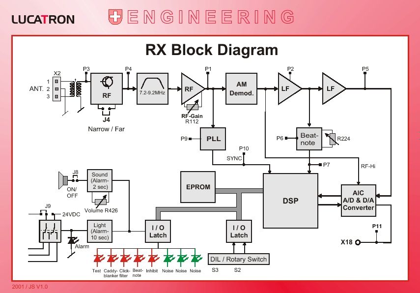
URB-100 Tuning Guide LUCATRON AG CH-8606 Greifensee, Switzerland Version 2 Page 1 R R X X T T U U N N I I N N G G G G U U I I D D E E URB-100 Tuning Guide LUCATRON AG CH-8606 Greifensee, Switzerland Version 2 Page 2 Table of Contents Page 1. Basic Description, Receiver Electronics.................................................................................3 1.1. Analog Part .....................................................................................................................3 1.2. Digital Part ......................................................................................................................3 1.3. Power / Alarm Part ...........................................................................................................4 2. Description of Features ............................................................................................................4 2.1. Manually Adjustable RF Gain..........................................................................................4 2.2. Air Synchronization .........................................................................................................4 2.3. Synchronous Demodulator..............................................................................................4 2.4. Beat Note Filter ...............................................................................................................4 2.5. Software Click Filter with Adaptive Slope ........................................................................4 2.6. Software Spike Blanker...................................................................................................4 2.7. Accept Counter ...............................................................................................................5 2.8. Threshold Calculation .....................................................................................................5 2.9. Alarm Threshold Margin Settings ....................................................................................5 3. Tuning........................................................................................................................................6 3.1. Philosophy ......................................................................................................................6 3.2. Recommended Tools ......................................................................................................6 3.3. Receiver Preparatory Steps ............................................................................................6 3.3.1. Preparation.........................................................................................................6 3.4. Receiver Tuning..............................................................................................................8 3.4.1. RF Gain Adjustment ............................................................................................8 3.4.2. Beat Note Adjustment .......................................................................................10 3.4.3. Signal / Noise Level Check ................................................................................11 3.4.4. DIL Switch Settings ..........................................................................................12 3.5. Alarm Adjustments ........................................................................................................12 3.6. Quick Check .................................................................................................................13 3.6.1. Basics ..............................................................................................................13 3.6.2. RF-Gain Check.................................................................................................13 3.6.3. Beat Note Check ...............................................................................................14 3.6.4. Signal / Noise Check .........................................................................................15 4. Appendix .................................................................................................................................16 4.1. Technical Specifications................................................................................................16 4.2. Tuning Flowchart ..........................................................................................................17 4.3. X3 Connector Layout (External Alarm Unit)...................................................................18 4.4. DIL Switch Settings .......................................................................................................19 4.5. Rotary Switch Settings ..................................................................................................20 4.6. Test Points....................................................................................................................21 4.7. Jumper Settings ............................................................................................................22 4.8. Compressed Overview..................................................................................................23 URB-100 Tuning Guide LUCATRON AG CH-8606 Greifensee, Switzerland Version 2 Page 3 1. Basic Description, Receiver Electronics The URB-100 receiver board consists of a: - Analog Part - Digital Part - Power / Alarm Part Analog Part Digital PartPower / Alarm Part + +- + GNDP3/RF P4/ RF GND GNDGND GND P1/RF P9 P2 P7 P6 R224 P5 P11 R112 P10 P8 S3 S2 ONOFF X18 R426 DSP J10 J4 J9 J8 J1 J3 J2 J5 J7 IN NC IN OUT NC OUT Power (X1) Relay (X3) Light (X4) Antenna (X2) X6 Fuse S1 X7 X5 (+ +) (- -) J6 WD R RF-Gain BeatBeatBeat Beat Beatnote Gain LF Video Video LF Sync Mod Volume 0 4 6 2 8 1 RLY NC NO GND Receiver Board 1.1. Analog Part The first input stage amplifies the received RF signal. If this signal is too large, the gain of the first input stage can b…
Text truncated - open the document above for the full version.
Users Manual
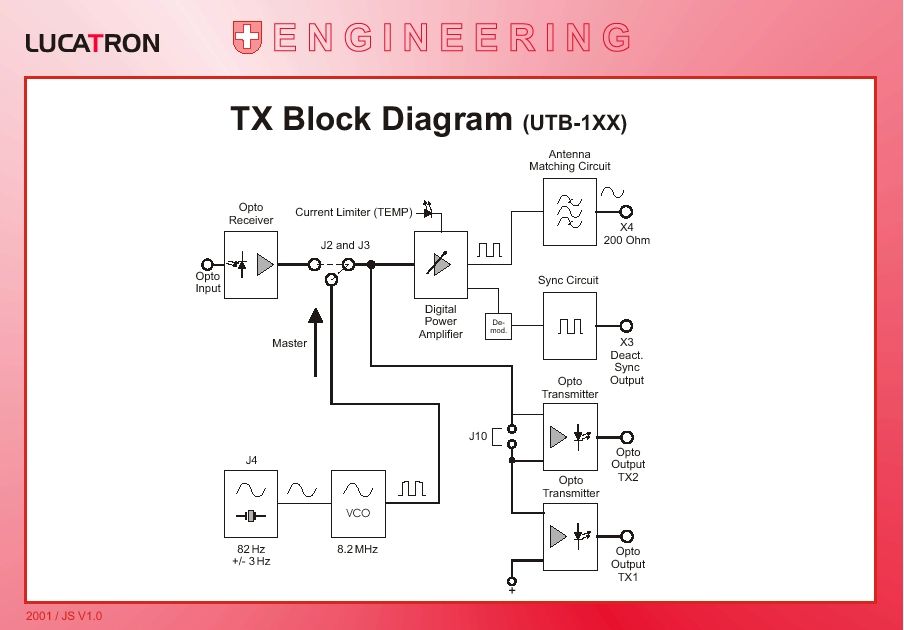
UTB-100 TX Tuning Guide LUCATRON AG CH-8606 Greifensee, Switzerland Version 1.0 Page 1 T T X X T T u u n n i i n n g g G G u u i i d d e e U U T T B B - - 1 1 0 0 0 0 A A UTB-100 TX Tuning Guide LUCATRON AG CH-8606 Greifensee, Switzerland Version 1.0 Page 2 Table of Contents Page 1. Introduction .................................................................................................................................3 1.1. Basic Description of the Transmitter Electronics...................................................................3 1.1.1. Digital Part ................................................................................................................6 1.1.2. Analog Part...............................................................................................................6 1.1.3. Power Supply / Filter Part .........................................................................................6 1.2. Receiver Electronics.............................................................................................................6 2. UTB-100 Filter Concept ...............................................................................................................7 3. Deactivator DAV-100 Synchronization .......................................................................................8 3.1. Cable Synchronization..........................................................................................................8 4. Opto TX Setup..............................................................................................................................9 4.1. One (1) Opto TX Output .......................................................................................................9 4.2. Two (2) Opto TX Output .......................................................................................................9 5. Installation Configurations .......................................................................................................10 6. Tuning ........................................................................................................................................12 6.1. Recommended Tools .........................................................................................................12 6.2. Preparation.........................................................................................................................12 6.3. Power On Adjustments.......................................................................................................14 7. Appendix ....................................................................................................................................15 7.1. Compressed Overview .......................................................................................................15 UTB-100 TX Tuning Guide LUCATRON AG CH-8606 Greifensee, Switzerland Version 1.0 Page 3 1. Introduction This manual describes the UTB-100 (Universal Transmitter Board) as well as the setup and tuning procedures needed to put the UTB-100 and URB-100 electronics into operation. For details on the receiver board, see the RX Tuning Guide. 1.1. Basic Description of the Transmitter Electronics Each transmitter electronics is able to feed one LUCATRON antenna with a swept HF signal of 8.2 MHz. In order to avoid disturbances between the emitted HF signals, synchronization with other transmitters must be guaranteed. The standard version of the UTB-100 board allows the 82 Hz sinusoidal modulated 8.2 MHz HF carrier signal to be: − −− − generated locally (oscillator circuit for master applications), or alternatively. − −− − to be regenerated from an optically received swept HF signal of another TX (opto receiver for slave applications). The bi-opto version of the UTB-100 additionally allows the onboard generated (master) or received- and-then-regenerated- (slave)-swept HF-signal to be converted and optically transmitted in order to synchronize additional transmitters. The two opto transmitters used in the bi-opto version allow: − −− − a master transmitter to synchronize two other optically slaved (and possibly repeating) transmitters. − −− − an optically slaved transmitter to be used as repeater to synchronize two other optically slaved transmitters. By using 3 bi-opto transmitter boards (TX) (one used as synchronization master and two as synchronization repeaters) and 4 standard TX (as synchronization slaves), clusters of up to 7 TX may be synchronized. This way up to 7 checkout or 14 exit-gates (in a row) may be configured without need of a master rack. Since the optically transmitted synchronization signal may be repeated only once, a master rack still has to be used if more than seven transmitters have to be synchronized. A block diagram and layout of the UTB-100 board are shown on the next 2 pages. The board consists of a digital part, an analog part and a power supply / filter part. The standard version of the UTB-100 is fully equipped with the exception of the two optional opto transmitters. It can be used as a master-TX for small installations (single or dual gates equipped with one TX only) or as slave-TX for all larger applications. The bi-opto version of the UTB-100 board is almost identical to the standard version. The only difference is that the two opto transmitters (IR-LED's) are already mounted. The bi-opto TX board can be used as a master-TX in medium installations (2 to 7 TX) or as synchronization signal repeating slave-TX for medium to very large installations. I NTRODUCTION UTB-100 TX Tuning Guide LUCATRON AG CH-8606 Greifensee, Switzerland Version 1.0 Page 4 VCO J4 82 Hz +/- 3 Hz 8.2 MHz Opto Transmitter Opto Transmitter Digital Power Amplifier Current Limiter (TEMP) Master Opto Receiver J2 and J3 Opto Output TX1 Opto Output TX2 Antenna Matching Circuit X4 200 Ohm J10 X3 Deact. Sync Output De- mod. Sync Circuit Opto Input + TX Board Block Diagram I NTRODUCTION UTB-100 TX Tuning Guid…
Text truncated - open the document above for the full version.
Cover Letter(s)
EAS Corporation 2843 Centerport Circle • Pompano Beach, Florida 33064 USA • US Toll Free: 800-331-4675 • Phone: 954-426-2965 • Fax: 954-426-8389 From: Richard Spagna To:FCC Subject: Confidentiality of Schematic Diagrams We request that you keep all of our schematic diagrams confidential. They are considered proprietary documents and we do not distribute them to anyone without a written non-disclosure agreement between our company and the recipient. These documents if published could allow other companies to copy our equipment. If you need more information regarding this request or if it is subject to being denied, please contact me via email at: [email protected] prior to it being posted publicly. Thank you, Richard Spagna President
Cover Letter(s)
From: Richard Spagna [email protected] To: Joe Dichoso [email protected] FCC Application Processing Branch Re: FCC ID P9WAQUILA Applicant: SenTech EAS Corporation Correspondence Reference Number: 23718 731 Confirmation Number: EA391720 Re Questions from: [email protected] Date: Tue Aug 20, 2002 12:58:22 PM US/Eastern To: [email protected] 1) The operational description indicates that the device has a digital part and an analog part. What does this mean? Does the device transmit in two different modulation types? What are the modulation types? 1. The system does not transmit in in two modulation types. The operational description was written in Switzerland and it is a language issue. What they meant is that the analog part is all of the circuitry except the Digital Signal Processor circuitry. It is FM frequency modulated only. 2) Provide a plot showing the signal sweeping throughout the operating frequency ranges. 2. see attached file. 3) Does the device sweep through the requested operating frequency range of 7.5-8.9 Mhz or does the device hop on specific frequencies throughout the operating frequency range? 3. It sweeps at an 82 Hz rate – see attached file. 4) It appears that the conducted output data shows levels above the 15.207 limits. Please explain. 4. We added filters and a ground to the PCB mounting plate – see attached file. 5) The device transmits on restricted band frequencies per 15.205. Please explain and indicate compliance. 5. see attached file.
ID Label/Location Info
SenTechEAS corporation 2843 CENTERPORT CIRCLE, POMPANO BEACH, FLORIDA U.S.A. PHONE: 954-426-2965 • FAX: 954-426-8389 4.000 2.000 R. SPAGNA 2/3/2002 SEE NOTES NONE 1 1 LABEL, FCC, "X"AISLE SYSTEM 2/3/2002 Aquila SWEPT RADIO FREQUENCY EAS SYSTEM MADE IN U.S.A. RATINGS: 18 VAC, 1.6A SERIAL NO: FCC ID: P9WAQUILA Thisdevicecomplieswithpart15oftheFCCrules.Operationissubjecttothe followingtwoconditions:(1)Thisdevicemustnotcauseharmfulinterference; and(2)Thisdevicemustacceptanyinterferencethatmaycauseundesired operation. SenTechEAS Corporation 2843 Centerport Circle, Pompano Beach, Florida 33064 U.S.A. Phone: 954-426-2965 Fax: 954-426-8389 www.sentecheas.com P9WAQUILA A DRAWING NUMBER REV MATERIAL CHECKED BY DATE TITLE DRAWN BY DATE SCALE SHEET OF THISDRAWINGMAYCONTAINPATENTEDOR PROPRIETARYINFORMATIONANDMUSTNOTBE USEDFORMANUFACTURINGORANYPURPOSE DETRIMENTALTOSENTECHCORPORATIONWITHOUT THEWRITTENCONSENTOFSENTECH CORPORATION.ACCEPTANCEOFTHISDRAWING WILLBECONSTRUEDASANAGREEMENTTOAND ACCEPTANCEOFTHEFORGOING. NOTES: 1. LETTERING IS TO BE APPROXIMATELY AS SHOWN, CENTERED ON LABEL. 2. MATERIAL - PRINTING IS TO BE 100% BLACK ON WHITE VINYL BACKED WITH ACRYLIC ADHESIVE.LAMINATE WITH IMPRINTABLE LAMINATION.
Operational Description
Article Security and Identification Aquila System, Theory of Operation LUCATRON AG, CH-8606 Greifensee, Switzerland Theory3.doc, 22-Apr-02, Page 1 of 2 1. Receiver Electronics The URB-100 receiver board consists of a: - Analog Part - Digital Part - Power / Alarm Part 1.1. Analog Part The first input stage amplifies the received RF signal. If this signal is too large, the gain of the first input stage can be reduced using jumper J4 (Narrow or Wide position). The next stage is a band-pass filter having a frequency range between 7.2 to 9.2 MHz. If necessary, the gain of the RF amplifier following the band-pass filter can be changed with potentiometer R112 (RF-Gain). An AGC is not built in, this gives a controlled RF amplification. The amplitude of the tag signal is pre-regulated by a fixed resistor. The DSP synchronization is done through "air", that is extracted from the received transmitter signal. A beat note circuit is implemented. This circuit is inhibiting spikes, radio transmitters and other signals with a very high Q factor. 1.2. Digital Part The analog tag signal is A/D converted and sampled. The DSP (40MIPS) filters the demodulated LF signal and stores the result in a memory. It processes this data and if all alarm criteria are met, it triggers an alarm. DIL and rotary octal switches allow adjusting the software parameters and test positions. 1.3. Power / Alarm Part Power is supplied to the receiver electronics by applying 20-26 VDC or 18-20 VAC to the power supply/power filter part. The integrated filter is used to reduce any interference picked up on the incoming line from the power supply. An audible alarm (buzzer) is mounted on the filter part. Outputs for the antenna lamp and an exter- nal alarm are provided. The volume of the buzzer is adjustable with the Volume potentiometer (R426). A jumper (J10) on the filter part allows setting the buzzer for continuous or intermittent tone. The duration of the audible alarm is about 2 seconds. The duration of the alarm light is about 10 seconds. Article Security and Identification Aquila System, Theory of Operation LUCATRON AG, CH-8606 Greifensee, Switzerland Theory3.doc, 22-Apr-02, Page 2 of 2 2. Description of the Transmitter Electronics Each transmitter electronics is able to feed one LUCATRON antenna with a swept HF signal of 8.2 MHz. In order to avoid disturbances between the emitted HF signals, synchronization with other transmitters must be guaranteed. The standard version of the Aquila TX board allows the 85 Hz sinusoidal modulated 8.2 MHz HF carrier signal to be: − generated locally (oscillator circuit for master applications), or alternatively − to be regenerated from an optically received swept HF signal of another TX (opto receiver for slave applications). The bi-opto version of the Aquila TX additionally allows the onboard generated (master) or received and then regenerated (slave) swept HF-signal to be converted and optically transmitted in order to synchronize additional transmitters. The two opto transmitters used in the bi-opto version allow: − a master transmitter to synchronize two other optically slaved (and possibly repeating) transmit- ters. − an optically slaved transmitter to be used as repeater to synchronize two other optically slaved transmitters. By using 3 bi-opto transmitter boards (TX) (one used as synchronization master and two as synchronization repeaters) and 4 standard TX (as synchronization slaves), clusters of up to 7 TX may be synchronized. This way up to 7 checkout or 14 exit-gates (in a row) may be configured with- out need of a master rack. Since the optically transmitted synchronization signal may be repeated only once, a master rack still has to be used if more than seven transmitters have to be synchronized. A block diagram and of the Aquila TX board are shown on the next pages. The board consists of a digital part, an analog part and a power supply / filter part. The standard version of the Aquila transmitter is fully equipped with the exception of the two optional opto transmitters. It can be used as a master-TX for small installations (single or dual gates equipped with one TX only) or as slave-TX for all larger applications. The bi-opto version of the Mark 4 transmitter board is almost identical to the standard version. The only difference is that the two opto transmitters (IR-LED's) are already mounted. The bi-opto TX board can be used as a master-TX in medium installations (2 to 7 TX) or as synchronization signal repeating slave-TX for medium to very large installations. 2001 / JS V1.0 E N G I N E E R I N GE N G I N E E R I N G LUCARONT LF 7.2-9.2MHz RF RF LF AM Demod. RX Block Diagram ANT. P4 P10 P7 P1 P3 P5 RF-Gain R112 PLL Beat- note J4 Narrow / Far X2 1 2 3 RF-Hi SYNC R224 EPROM DSP AIC A/D & D/A Converter P11 DIL / Rotary Switch Test Caddy- blanker Inhibit Noise Noise Noise I / O Latch J8 ON/ OFF Volume R426 J9 24VDC Alarm X18 Sound (Alarm- 2 sec) Light (Alarm- 10 sec) S3S2 P2 P6 Click- filter Beat- note I / O Latch P9 LF VCO J4 82 Hz +/- 3 Hz 8.2 MHz Opto Transmitter Opto Transmitter Digital Power Amplifier Current Limiter (TEMP) Master Opto Receiver J2 and J3 Opto Output TX1 Opto Output TX2 Antenna Matching Circuit X4 200 Ohm J10 X3 Deact. Sync Output De- mod. Sync Circuit Opto Input + TX Block Diagram (UTB-1XX) 2001 / JS V1.0 E N G I N E E R I N GE N G I N E E R I N G LUCARONT
Test Report
Technical Report No. 01-087a EMI Research and Development Laboratory Department of Electrical Engineering Florida Atlantic University 3998 FAU Blvd, Suite 310 Boca Raton, Florida 33431 (561) 338-1650 Technical Report No. 01-087a "EMI Evaluation of the SENTECH EAS CORP AQUILA to FCC Part 15 Class A Conducted and Radiated Emission Requirements." Performed: 2 November 2001 Customer: SENTECH EAS CORP Attn: Richard Spagna 2843 Centerport Circle Pompano Beach, Florida 33064 Company Official responsible for product tested:_____________________________ Richard Spagna Tel. (954-426-2965 ext.19) Performed and Reported by: _______________________________ Lynne Carmody FAU EMI R & D Laboratory 1. INTRODUCTION Technical Report No. 01-087a 2 The SENTECH EAS CORP Aquila Model No. AQA-100 for receiving, and Model No. AQA-200 for transmitting was evaluated for conformance to FCC requirements identified below. The Aquila received power from a power supply Model STC 8200- P. Evaluation results reported in this 13 page document apply only to the specific items of equipment, configurations (including software and unit operation), and procedures supplied to the Florida Atlantic University EMI Research Lab by SENTECH EAS CORP under the test conditions listed herein. 2. OBJECTIVE This evaluation was performed to verify conformance of the SENTECH EAS CORP Aquila with reference to the U.S. Federal Communications Commission (FCC) Code of Federal Regulations (CFR), Title 47 - Telecommunication, Part 15 - Radio Frequency Devices, Subpart B - Unintentional Radiators, Section 15.107(b) Conducted limits, Section 15.109(b) Radiated Emission limits and Section 15.223 Operation in the Band 1.705-10 MHz. 3. CONCLUSION The SENTECH EAS CORP Aquila met conducted and radiated emission requirements as described in the following test result section. 4.0 TEST PROCEDURES AND RESULTS 4.1 TEST PROCEDURES The measurement techniques identified in measurement procedure ANSI C63.4-2001 "American National Standard of Measurement of Radio-Noise Emissions from Low-Voltage Electrical and Electronic Equipment in the Range of 9 kHz to 40 GHz" were followed as close as practical during this evaluation. Complete details and specific procedures used are discussed in the respective Tests Results sections. Technical Report No. 01-087a 3 4.2 TEST RESULTS 4.2.1 CONDUCTED POWERLINE EMISSIONS The SENTECH EAS CORP Aquila Model No. AQA-100 for receiving, and Model No. AQA-200 was set up at the FAU EMI Research facilities conducted emissions shielded enclosure. The equipment as a pair was placed on the floor and 40 centimeters from the rear wall of the RF shielded room as defined in the referenced FCC adopted measurement procedure ANSI C63.4-2001. Photograph 1 shows the physical positioning of the SENTECH EAS CORP Aquila and associated power supply during the conducted emissions test. The SENTECH EAS CORP Aquila was powered by a power supply Model STC8200-P which was plugged into a Solar model 8028-50, 50 Ω / 50 μH Line Impedance Stabilization Network (LISN). Conducted power line emissions were measured on both the phase and neutral lines in reference to earth ground over the specified 450 kHz to 30 MHz range on a Hewlett Packard HP 8566B Spectrum Analyzer. The spectrum analyzer was operated in the peak detector mode with a bandwidth of 9 kHz obtained through an HP 85650A Quasi-Peak Adapter. The HP 85864C EMI test program collected the conducted emissions over the specified frequency range and plotted the results. Figures 1 and 2 show the peak detected conducted emissions from the SENTECH EAS CORP Aquila was below the FCC Class A conducted emission limit over the entire specified frequency range. A quasi peak was performed on both phase and neutral lines showing a 1-3 dB drop in the area close to the limit. Technical Report No. 01-087a 4 PHOTOGRAPH 1: CONDUCTED EMISSIONS TEST SETUP Technical Report No. 01-087a 5 FIGURE 1: CONDUCTED EMISSION LEVELS (PHASE LINE) Technical Report No. 01-087a 6 FIGURE 2: CONDUCTED EMISSION LEVELS (NEUTRAL LINE). Technical Report No. 01-087a 7 4.2.2 RADIATED EMISSIONS The SENTECH EAS CORP Aquila unit was set up on a wooden turntable 80 centimeters above the ground plane of the FCC listed Semi-Anechoic test site. The radiated emission test was performed with the Aquila powered by a power supply Model STC-8200-P. An EMCO 3104 Broadband Biconical antenna was installed on an EMCO pneumatically controlled Antenna Mast at a distance of 3 meters from the system. The 30 to 200 MHz frequency range was automatically scanned on the HP 8566B Spectrum Analyzer operated in the peak detector mode with a bandwidth of 120 kHz obtained through the HP 85650A Quasi Peak Adapter. The turntable was incrementally rotated through 360 degrees, the antenna was scanned in height from 1 to 4 meters in both the horizontal and vertical polarizations. An EMCO 3146 Log Periodic antenna was then installed and the above procedure was repeated for the 200 to 1000 MHz range. Photographs 2 and 3 show the physical positioning of the Aquila and associated power supply during the radiated emissions test. Figures 3 and 4 show the composite plot of the worst-case level radiated emissions in peak detector mode, at horizontal and vertical polarization between 30-200 MHz, independent of azimuth. Figures 5 and 6 show the composite plot of the worst -case level radiated emissions in peak detector mode, at horizontal and vertical polarization between 200-1000 MHz, independent of azimuth. The frequency band of operation is 7.47 to 9.00. The worst emission was determined to be at 8.9 MHz. The unit under test was brought out to the 30 ft. by 70 ft. Open Field 10 meter Test Site and measurements were done at the maximum azimuth with a loop antenna model no. ALR 25M , see Photograph 4. The data was extrapolated to 30 meters as per Section 15.223 restricting the field strength of any emission to 100 μV/m at a distance of 30 meters. The antenna factor is 42 dB/m and the amplifier…
Text truncated - open the document above for the full version.
Test Report
Technical Report No. 01-087a EMI Research and Development Laboratory Department of Electrical Engineering Florida Atlantic University 3998 FAU Blvd, Suite 310 Boca Raton, Florida 33431 (561) 338-1650 Technical Report No. 01-087a "EMI Evaluation of the SENTECH EAS CORP AQUILA to FCC Part 15 Class A Conducted and Radiated Emission Requirements." Performed: 2 November 2001 Customer: SENTECH EAS CORP Attn: Richard Spagna 2843 Centerport Circle Pompano Beach, Florida 33064 Company Official responsible for product tested:_____________________________ Richard Spagna Tel. (954-426-2965 ext.19) Performed and Reported by: _______________________________ Lynne Carmody FAU EMI R & D Laboratory 1. INTRODUCTION Technical Report No. 01-087a 2 The SENTECH EAS CORP Aquila Model No. AQA-100 for receiving, and Model No. AQA-200 for transmitting was evaluated for conformance to FCC requirements identified below. The Aquila received power from a power supply Model STC 8200- P. Evaluation results reported in this 13 page document apply only to the specific items of equipment, configurations (including software and unit operation), and procedures supplied to the Florida Atlantic University EMI Research Lab by SENTECH EAS CORP under the test conditions listed herein. 2. OBJECTIVE This evaluation was performed to verify conformance of the SENTECH EAS CORP Aquila with reference to the U.S. Federal Communications Commission (FCC) Code of Federal Regulations (CFR), Title 47 - Telecommunication, Part 15 - Radio Frequency Devices, Subpart B - Unintentional Radiators, Section 15.107(b) Conducted limits, Section 15.109(b) Radiated Emission limits and Section 15.223 Operation in the Band 1.705-10 MHz. 3. CONCLUSION The SENTECH EAS CORP Aquila met conducted and radiated emission requirements as described in the following test result section. 4.0 TEST PROCEDURES AND RESULTS 4.1 TEST PROCEDURES The measurement techniques identified in measurement procedure ANSI C63.4-2001 "American National Standard of Measurement of Radio-Noise Emissions from Low-Voltage Electrical and Electronic Equipment in the Range of 9 kHz to 40 GHz" were followed as close as practical during this evaluation. Complete details and specific procedures used are discussed in the respective Tests Results sections. Technical Report No. 01-087a 3 4.2 TEST RESULTS 4.2.1 CONDUCTED POWERLINE EMISSIONS The SENTECH EAS CORP Aquila Model No. AQA-100 for receiving, and Model No. AQA-200 was set up at the FAU EMI Research facilities conducted emissions shielded enclosure. The equipment as a pair was placed on the floor and 40 centimeters from the rear wall of the RF shielded room as defined in the referenced FCC adopted measurement procedure ANSI C63.4-2001. Photograph 1 shows the physical positioning of the SENTECH EAS CORP Aquila and associated power supply during the conducted emissions test. The SENTECH EAS CORP Aquila was powered by a power supply Model STC8200-P which was plugged into a Solar model 8028-50, 50 Ω / 50 μH Line Impedance Stabilization Network (LISN). Conducted power line emissions were measured on both the phase and neutral lines in reference to earth ground over the…
Text truncated - open the document above for the full version.
Contact Information
Applicant
Richard J Spagna(President)
Technical Contact
SenTech EAS CorporationRichard J Spagna
[email protected]954-426-2965
2843 Centerport Circle · Pompano Beach, Florida · United States
Test Firm
Florida Atlantic UniversityVichate Ungvichian
Technical Specifications
| # | Rule Parts | Frequency Range | Power Output |
|---|---|---|---|
| 1 | 15C | 7.5 MHz - 8.9 MHz | - |