POW9000V5Nonbroadcast VHF Transceiver
DX Radio Systems Inc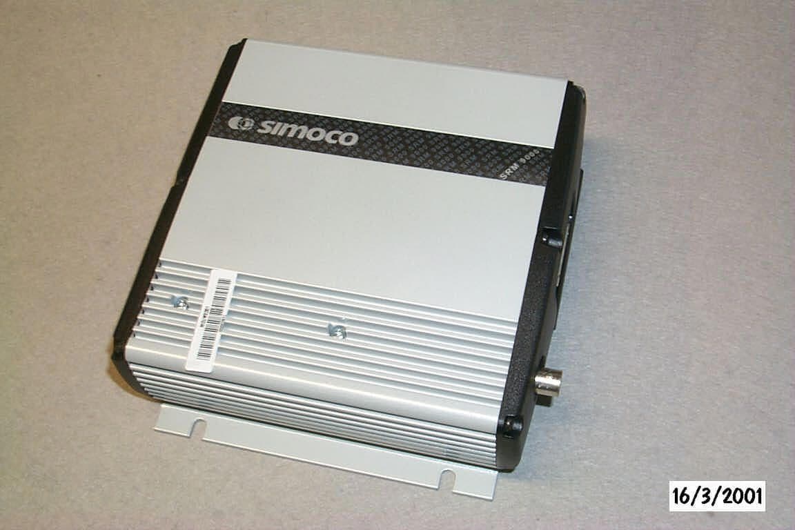
Click to zoom
Application Details
- Equipment Class
- TNB - Licensed Non-Broadcast Station Transmitter
- Date of Grant
- Aug 16, 2001
- Application Purpose
- Original Equipment
- Date of Application
- Jun 18, 2001
- Equipment Note
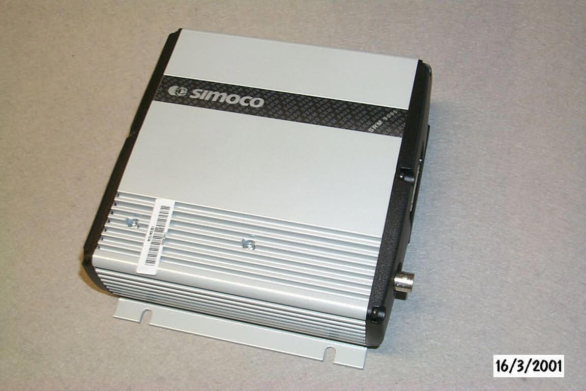
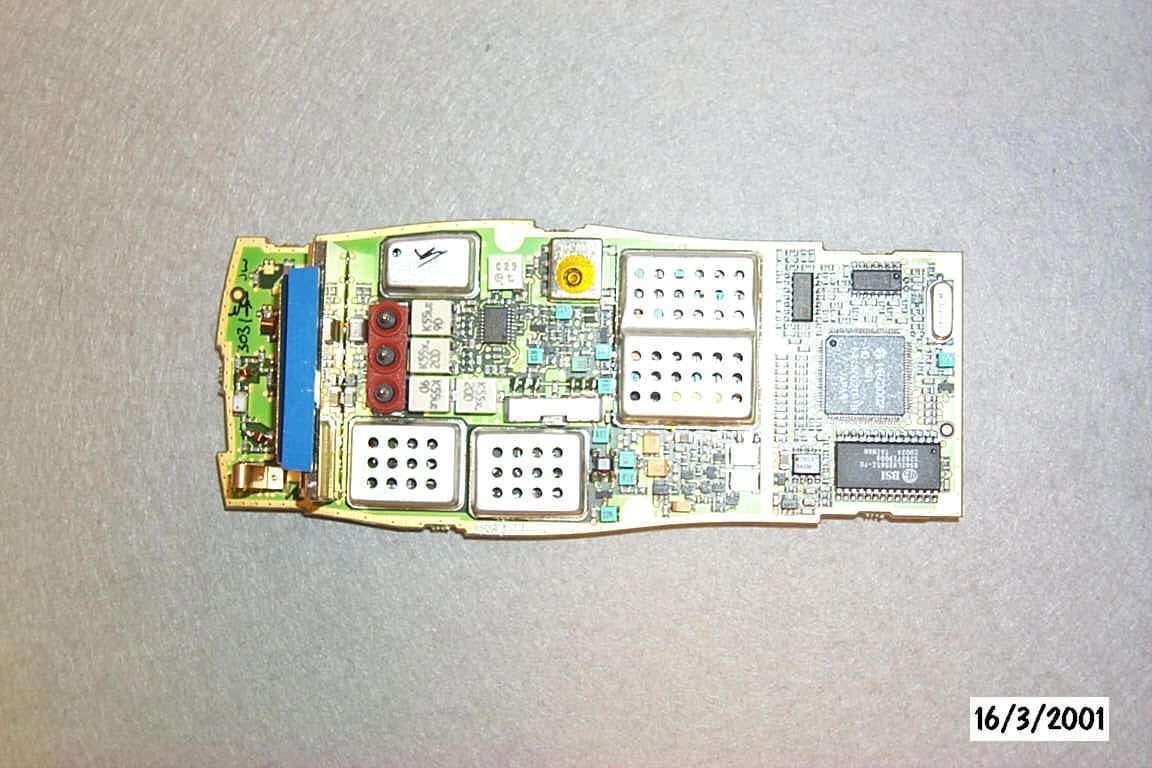
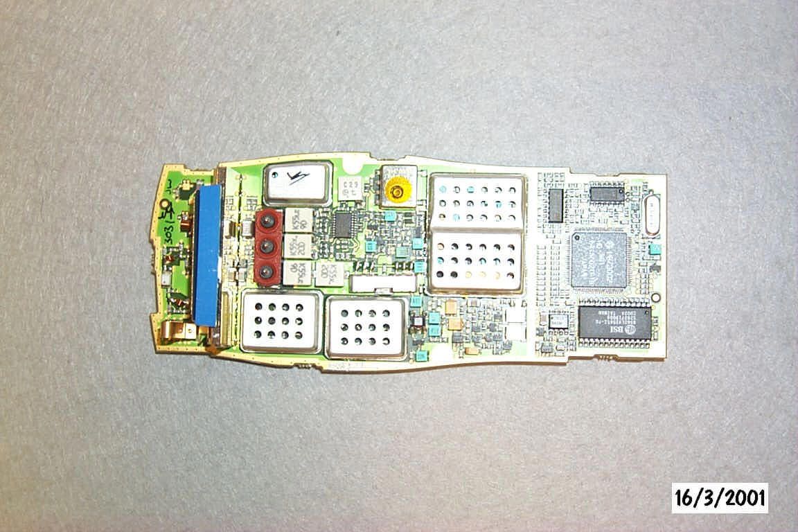
- Nonbroadcast VHF Transceiver
- Frequency Range
- 216.00000000 - 222.00000000
- Company
- DX Radio Systems Inc
- Country
- United States
Documents & Files
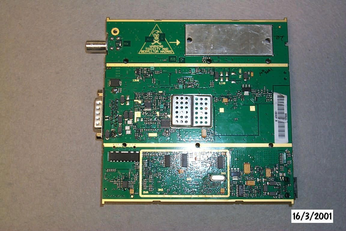
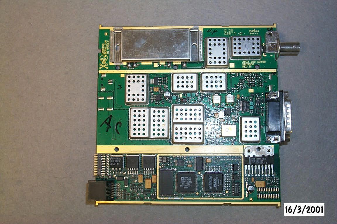
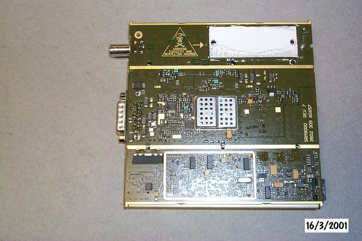
Document Text
Text extracted from the exhibit documents filed with the FCC. Open a document above to read the original.
Users Manual
SRM 9000 Series FM VHF/UHF Mobile Radio Transceiver SERVICE MANUAL TNM-M-E-0001 October 2000 Draft D abcde abcde DRAFT D TNM-M-E-0001Page ii Revision History RevisionEditorDateRevision Details 1.0J. McB30/03/2000Initial Release Draft AA.G.June 2000Partial re-format to Simoco Europe standard. Draft BP.N.04/07/2000Rev6 Schematics, UW Band & Appendix updates Draft CP.N.31/07/2000Still in progress – not to be released! Updated with E0,AC,TK,UW rev7 schematics & layouts Revised Block Diagram. 9010 mic, corrected alignment instructions Draft C5A.G.17-07-2000Update to Draft C from Simoco Pacific. Draft DA.G.27-09-2000Amended text: Variants; Tech Spec & App B. List of Associated Publications Document No.DescriptionIssued By TNM-I-E-0005SRM9000 Series Installation InstructionsSimoco Europe TNM-U-M-0001SRM9010 PMR/Trunk Operating InstructionsSimoco Europe TNM-U-E-0013SRM9020 PMR Operating InstructionsSimoco Europe TNM-U-E-0014SRM9025 PMR Operating InstructionsSimoco Europe TNM-U-E-0015SRM9025 Trunk Operating InstructionsSimoco Europe TNM-U-E-0003SRM9030 PMR Operating InstructionsSimoco Europe TNM-U-E-0004SRM9030 Trunk Operating InstructionsSimoco Europe DRAFT D TNM-M-E-0001Page iii Table of Contents 1.INTRODUCTION............................................................................................................1 1.1GENERAL........................................................................................................................1 1.2SCOPE...........................................................................................................................1 1.3DESCRIPTION..................................................................................................................1 1.4PRODUCT VARIANTS AND FACILITIES...............................................................................2 1.5GLOSSARY......................................................................................................................5 2.SERVICE PHILOSOPHY...............................................................................................6 2.1SERVICE CONCEPT.........................................................................................................6 2.2WARRANTY.....................................................................................................................6 2.2.1Service within and out of warranty........................................................................6 2.2.2Ancillary Items.......................................................................................................6 2.3SOFTWARE POLICY.........................................................................................................6 2.4ADJUSTMENT AND ALIGNMENT.........................................................................................7 2.5TECHNICAL SPECIFICATION..............................................................................................8 2.5.1General.................................................................................................................8 2.5.2Transmitter............................................................................................................9 2.5.3Receiver..............................................................................................................10 2.5.4Signalling.............................................................................................................11 2.5.5Environmental.....................................................................................................12 3.TECHNICAL DESCRIPTION.......................................................................................13 3.1RECEIVER.....................................................................................................................13 3.1.1Front End Filters and RF Amplifier......................................................................13 3.1.2First Mixer and IF Section...................................................................................13 3.1.3Quadrature Demodulator....................................................................................15 3.1.4Receiver Audio Processing.................................................................................15 3.2TRANSMITTER...............................................................................................................15 3.2.1Drivers and PA Stages........................................................................................15 3.2.2Power Control.....................................................................................................17 3.2.3Antenna Changeover and Harmonic Filter..........................................................17 3.2.4Transmitter Audio Processing.............................................................................17 3.3FREQUENCY SYNTHESISER............................................................................................19 3.3.1General...............................................................................................................19 3.3.2PLL......................................................................................................................19 3.3.3VCO....................................................................................................................19 3.3.4Negative Bias Generator and Loop Filter............................................................19 3.3.5Phase Modulator.................................................................................................19 3.3.6Reference Oscillator...........................................................................................20 3.4CONTROL.....................................................................................................................20 3.4.1DSP and FPGA...................................................................................................20 3.4.2DSP Clock Oscillator.................…
Text truncated - open the document above for the full version.
Block Diagram
DRAFT D TNM-M-E-0001 Page 16 Figure 3-2 VHF/UHF Transmitter Block Diagram An active filter comprising Q14, 17,18 and 19 provides isolation to minimise power supply noise at the PA. This is achieved by maintaining a voltage differential of approximately 1V across Q14 and indirectly filtering its gate voltage. Q14 is switched on only during transmit via R523 to minimise receiver power requirements. 9 0 0 0 _ 1 7 T x / R x S w i t c h D 6 1 0 / 6 1 1 T x V C O Q 6 0 2 T x V C O S w i t c h Q 6 0 3 T x B u f f e r / A m p Q 6 0 6 / 6 0 9 / 6 1 2 P o w e r C o n t r o l Q 3 / 1 0 V C O B u f f e r Q 6 0 4 / 6 0 5 S y n t h e s i s e r B u f f e r Q 6 0 7 T x P A D r i v e r Q 1 2 C o m p a r a t o r U 3 A Q 1 5 / 1 6 T X P A U 2 T x P A F i l t e r / S w i t c h Q 1 4 / 1 7 / 1 8 / 1 9 P o w e r C o n t r o l D e t e c t o r D 6 B u f f e r U 3 B A n t e n n a S w i t c h D 3 / 4 / 5 A n t e n n a F i l t e r L 1 0 / 1 1 / 1 2 R x A F S w i t c h U 1 0 3 C A D C / D A C C O D E C U 8 0 0 F r o m F P G A / D S P R x A F T X M O D 1 V C O C o n t r o l V o l t s C P P T o R x M i x e r L O 1 R x t o U 7 0 1 R x / T x A F S w i t c h U 1 0 3 B M i c A m p Q 8 1 2 F r o m I Q D e m o d u l a t o r U 4 0 1 Q I M O D 1 O N ( T x / R x A F C o n t r o l ) T x P o w e r S e t F r o m M u l t i p l e x e r U 9 0 2 G a t e T x M i c A u d i o T x O p t i o n s A u d i o + D a t a A U D I N 2 A U D I N 1 F r o m F P G A S Y N T H G a t e U 1 0 7 G a t e U 1 0 8 I n v e r t e r Q 2 0 DRAFT D TNM-M-E-0001 Page 14 Figure 3-1 VHF/UHF Receiver Block Diagram 9 0 0 0 _ 1 6 A n t e n n a S w i t c h D 3 , D 4 & D 5 A n t e n n a F i l t e r L 1 0 , L 1 1 & L 1 2 9 0 M H z L . O . Q 4 0 2 R x V C O Q 6 0 0 R x V C O S w i t c h Q 6 0 1 V C O B u f f e r Q 6 0 4 / 6 0 5 S y n t h e s i s e r B u f f e r Q 6 0 7 t o U 7 0 1 T o T x B u f f e r t o U 7 0 1 T o T x P A C P P V C O C o n t r o l V o l t s R x P S U T x / R x S w i t c h D 6 1 0 / 6 1 1 R x / T x A F S w i t c h U 1 0 3 B M i c A m p Q 8 1 2 B a n d p a s s F i l t e r R F A m p Q 4 0 0 B a n d P a s s F i l t e r M i x e r T 4 0 0 I F A m p Q 4 0 1 S p e a k e r A m p U 5 S p k r S w i t c h Q 8 1 0 / 8 1 1 / 8 1 3 4 - P o l e 4 5 M H z F i l t e r s Z 4 0 1 / 4 0 2 A F A m p U 8 0 3 A u x A F O / P A m p U 8 0 3 I Q D e m o d u l a t o r U 4 0 1 R x A F S w i t c h U 1 0 3 C A G C B u f f e r U 9 0 1 B A D C / D A C C O D E C U 8 0 0 F r o m M u l t i p l e x e r U 9 0 2 T u n e 1 , 2 , 3 & 4 Q I A F C / R e f O S C / M O D A u d i o I n F r o m M i c A u d i o o r O p t i o n A u d i o F r o m M u l t i p l e x e r U 9 0 2 F r o m F P G A / D S P A U D O u t S P K R O N S P K R O U T 1 S P K R O U T 2 T X M O D 1 T o T X V C O S Y N T H A U X C P DRAFT D TNM-M-E-0001 Page 21 Figure 3-4 VHF/UHF Control Block Diagram 9 0 0 0 _ 1 5 C l o c k Q 1 0 0 R e s e t U 1 0 1 D S P U 1 0 2 F P G A U 1 0 6 F l a s h M e m o r y U 1 0 4 S y n t h e s i s e r U 7 0 1 L o o p V o l t s R a m p G e n U 1 0 5 C A D C / D A C C O D E C U 8 0 0 M u l t i p l e x e r U 9 0 2 T x P o w e r C o n t r o l B u f f e r U 8 0 2 B M O V E X L o o p V o l t s M U X E N M U X A O M U X A 1 A U X C T L F E T u n e F r o n t E n d T u n e B u f f e r U 9 0 1 A F r o n t E n d V a r i c a p N e g V o l t s L e v e l T r a n s l a t o r Q 9 0 0 / 9 0 1 / 9 0 2 / 9 0 9 R x D a t a T x D a t a S e r i a l P o r t S e r i a l P o r t A G C T x P o w e r S e t A T o n e A D C R e f T u n e 1 - 4 T x D a t a B u f f e r Q 1 DRAFT D TNM-M-E-0001 Page 18 Figure 3-3 VHF/UHF Synthesiser, Block Diagram L o o p F i l t e r C 7 3 4 / 7 1 9 / 7 2 2 9 0 M H z L O Q 4 0 2 S y n t h e s i s e r U 7 0 1 L O 2 T o I Q D e m o d u l a t o r U 4 0 1 A U X L O 2 A U X C P C P P C P P F S Y N T H D O U T V C A P B I A S V C O N e g B i a s S u p p l y Q 7 0 0 / 7 0 1 / 7 0 2 / 7 0 3 R x / T x V C O Q 6 0 0 / 6 0 2 V C O B u f f e r Q 6 0 4 / 6 0 5 T x / R x S w i t c h D 6 0 1 / 6 1 1 T o R x M i x e r L O 1 R x T o T x B u f f e r S y n t h B u f f e r Q 6 0 7 F r o m F P G A T x M O D S w i t c h U 1 0 3 A R x / T x A F S w i t c h U 1 0 3 B M i c A m p Q 8 1 2 I A F C I N M O D 1 O N T x M O D 1 A D C / D A C C O D E C U 8 0 0 Q R e f O S C U 7 0 0 A F C A m p U 8 0 2 A A F C 9 0 0 0 _ 1 4 F r o m F P G A / D S P D i v i d e r U 7 1 0 3 6 ( U H F ) 7 2 ( V H F ) B u f f e r Q 7 1 0 F X T A L P h a s e M o d u l a t o r Q 7 1 4 / 7 1 5 / 7 1 6 R a m p G e n Q 7 1 1 / 7 1 2 / 7 1 3 B u f f e r U 7 1 1 / B L o w P a s s F i l t e r U 7 1 1 / A T x M o d 1 T u n e B a l G a t e U 1 0 7 G a t e U 1 0 8 A u d i n 1 M i c A u d i o O p t i o n A u d i o a n d D a t a I n p u t
ID Label/Location Info
FCC ID label for DXM9000 Model: DXM9000 SERIES Mobile transceiver FCC ID: POW9000V5 Serial Number: ______________________ This device complies with Part 15 of the FCC Rules. Operation is subject to the condition that this device does not cause harmful interference. Frequencies or channels programmed: Web page: dxradiosystems.com DX Radio S y stems , Inc. , US A 3.90 typ. 0.925 typ.
ID Label/Location Info
DXM9000 SERIES
Operational Description
DRAFT D TNM-M-E-0001 Page 13 3. Technical Description 3.1 Receiver Refer Figure 3-1 3.1.1 Front End Filters and RF Amplifier The receiver input signal from the antenna passes through the antenna filter comprising L10, L11, L12 and associated tuning capacitors. With the mobile in receive mode, diodes D3, D4 and D5 in the antenna switch are reverse biased allowing the receiver input signal to be coupled through to the front end with minimal loss. The overall insertion loss of the antenna filter and switch is approximately 0.8dB. Front end selectivity is provided by varactor tuned bandpass filters at the input and output of the RF amplifier. Front end tuning voltages are derived from the alignment data stored in the radio. The DSP processes this data to optimise front end tuning relative to the programmed channel frequencies which may be changed at any time without re-aligning the radio. To achieve the required varactor tuning range an arrangement of positive and negative bias power supplies is used to provide a total bias across the varactors of up to 14.0VDC. A fixed 2.5V positive bias derived from the 5.0V supply and voltage divider R425/426 is applied to the cathodes of the varactor diodes. The negative bias supply originates at the DSP/FPGA as a composite digital tuning signal (FE TUNE) containing the data for the four front end tuning values TUNE 1 to 4 for the particular channel frequency selected. The level is dependent on channel frequency and tuning and varies between +0.1 and +3.0V. This signal then passes through buffer U901A and level translator Q900 to Q903 where it is converted to a high level (- 0.5 to -11.5V) negative equivalent of the original signal. The -12.0V rail of the level translator is generated by U300B/C with D304 to D306 providing the required voltage multiplier effect. The high level negative signal is then split into the four individual front end negative DC values under software control by multiplexer U902 and associated storage capacitors C904 to C907 before being applied to the anodes of the front end tuning varactors. The RF amplifier stage comprises a low noise transistor amplifier (Q400) which is compensated to maintain good linearity across the required frequency bands and temperature range. This provides excellent intermodulation and blocking performance across the full operating range. The gain of this stage is typically 17dB for both UHF and VHF versions. 3.1.2 First Mixer and IF Section The output of the last front end bandpass filter is coupled into single balanced mixer T400/D413 which converts the RF signal to an IF frequency of 45MHz. The local oscillator injection level is typically +8dBm at T400 pin 1 with low side injection used for UHF and high side for VHF. Following the mixer is IF amplifier Q401 which provides approximately 15dB of gain and in association with its output circuitry presents the required load conditions to the 4 pole 45MHz crystal filter Z401/402. DRAFT D TNM-M-E-0001 Page 14 Figure 3-1 VHF/UHF Receiver Block Diagram 9 0 0 0 _ 1 6 A n t e n n a S w i t c h D 3 , D 4 & D 5 A n t e n n a F i l t e r L 1 0 , L 1 1 & L 1 2 9 0 M H z L . O . Q 4 0 2 R x V C O Q 6 0 0 R x V C O S w i t c h Q 6 0 1 V C O B u f f e r Q 6 0 4 / 6 0 5 S y n t h e s i s e r B u f f e r Q 6 0 7 t o U 7 0 1 T o T x B u f f e r t o U 7 0 1 T o T x P A C P P V C O C o n t r o l V o l t s R x P S U T x / R x S w i t c h D 6 1 0 / 6 1 1 R x / T x A F S w i t c h U 1 0 3 B M i c A m p Q 8 1 2 B a n d p a s s F i l t e r R F A m p Q 4 0 0 B a n d P a s s F i l t e r M i x e r T 4 0 0 I F A m p Q 4 0 1 S p e a k e r A m p U 5 S p k r S w i t c h Q 8 1 0 / 8 1 1 / 8 1 3 4 - P o l e 4 5 M H z F i l t e r s Z 4 0 1 / 4 0 2 A F A m p U 8 0 3 A u x A F O / P A m p U 8 0 3 I Q D e m o d u l a t o r U 4 0 1 R x A F S w i t c h U 1 0 3 C A G C B u f f e r U 9 0 1 B A D C / D A C C O D E C U 8 0 0 F r o m M u l t i p l e x e r U 9 0 2 T u n e 1 , 2 , 3 & 4 Q I A F C / R e f O S C / M O D A u d i o I n F r o m M i c A u d i o o r O p t i o n A u d i o F r o m M u l t i p l e x e r U 9 0 2 F r o m F P G A / D S P A U D O u t S P K R O N S P K R O U T 1 S P K R O U T 2 T X M O D 1 T o T X V C O S Y N T H A U X C P DRAFT D TNM-M-E-0001 Page 15 3.1.3 Quadrature Demodulator Additional IF gain of approximately 30dB occurs at U401 which is a dedicated IF AGC amplifier/Quadrature Demodulator configured for single ended input and output operation. The AGC voltage for U401 is derived from the RSSI function of the DSP via AUX CTL and multiplexer U902. The onset of AGC operation occurs when RF input signal levels at the antenna exceed -90dBm. Conversion of the 45MHz IF signal to I and Q baseband signals is carried out by the demodulator section of U401. The 90MHz local oscillator signal is generated by VCO Q402 which is phase locked by the auxiliary PLL output of U701 via feedback signal AUX LO2. 3.1.4 Receiver Audio Processing All receiver audio processing and filtering functions are performed by the CODEC U800 under the control of the DSP. The receiver I and Q analog baseband signals are converted to digital signals by the CODEC ADC before being applied to a series of digital filters which provide the final stage of adjacent channel filtering, high pass and low pass filtering and mute noise processing for narrow and wideband operation. The processed signals are then converted to analog audio signals by the CODEC DAC and are applied to conventional audio amplifiers U803A/B and the speaker amplifier U5. There are two speaker options available. A half bridged configuration using a speaker across balanced output SPKR OUT1 and 2 which provides an audio output level of up to 4 watts into 4 ohms. The other option is a full bridge configuration using a high power speaker across SPKR OUT1 and 2 and providing an audio output level of up to 10 watts into 8 ohms. The carrier and signalling mute functions are performed by Q810/811/813 under DSP control with additional receiver muting to U803B…
Text truncated - open the document above for the full version.
Parts List/Tune Up Info
DRAFT D TNM-M-E-0001 Page 25 4. Alignment This procedure is applicable to all versions of SRM9000 mobile transceivers. If the radio contains customer configuration data that must be retained, you must first use the SRM9000 Configuration Programmer (FPP) software to read the radio and store the data on an FPP file before commencing with the alignment procedure. When the Alignment is completed, use the SRM9000 Configuration Programmer (FPP) software to retrieve this stored data from the FPP file and write it back to the radio. It is preferred that the radio remain installed in its aluminium extruded case throughout this alignment procedure. If the radio is to be aligned when removed from the case, a temporary heat sink must be fitted under the Transmitter PA module and the receiver output must be kept below 100 mW. 4.1 TEST EQUIPMENT 1.Radio transceiver test setCMT, 52/82 or similar. 2.Variable DC power supply10.8V to 16.2V at 10 amps 3.Oscilloscope20 MHz bandwidth minimum 4.SRM9000 Programming & Alignment Breakout Box As detailed in Figure 4-1 5.SRM9000 Speaker O/P Breakout BoxAs detailed in Figure 4-2 6.Personal Computer486 DX 66 or better. Operating system Windows 95 or later. Minimum RAM - 16MB. 5MB free hard disk space. Floppy drive - 1.44MB. Mouse and serial port required 7.SRM9000 Alignment ToolComputer Software file 8.SRM9000 Configuration Programmer (FPP)Computer Software file Caution Preparing the radio will erase from the radio all customer PMR and Trunking configuration data (channel, signalling information etc). The only data retained by the Alignment Tool is the alignment data from the radio (DAC settings for TX power, front-end tuning etc). DRAFT D TNM-M-E-0001 Page 26 Black Red Yellow Blue Brown Orange Green(4) White (8) (Not Used) + 470E White Green Mic Audio in Mic Ground Ground Handset AF Output 13.8V Switched On/Off Rx Data Tx Data 8 4 7 6 5 3 2 1 RJ45 PRM80 Programming Cable P/N 9525-001-00016 BNC (F) Connector 22uF to 47uF Tant. or Elect DB25 Access and modify cable as shown 9000_49/2 2 5 - 9 W a y A d a p t o r PC To SRM9000 S1 AF Generator Figure 4-1 SRM9000 Programming & Alignment Breakout Box Figure 4-2 SRM9000 Speaker Output Breakout Box T1 600E 1:1 Line Matching Transformer To Noise & Distortion Meter & CRO To SRM9000 P2 Pins 6 & 13 9000_49/3 R R = Audio Power Load (set as appropriate) or Resistor 4E 4W for 1/2 Bridge Speaker option Resistor 8E 12W for full Bridge Speaker option DRAFT D TNM-M-E-0001 Page 27 4.2 test set up 7 6 5 4 3 2 1 8 15 14 13 12 11 10 9 SRM9000 P2 (DB15M) PC SRM9000 Programming and Alignment Breakout Box S5 Antenna Skt S1 RJ45 AF Generator 13.8V DC Power Supply CRO 9000_49 + - Radio Transceiver Test Set Noise & Distortion Meter SRM9000 Speaker O/P Breakout Box Coax (<200 mm) Figure 4-3 Test Set up 1. Connect the radio to the test equipment as shown in Figure 4-3. 2. Switch on the DC Power Supply. DRAFT D TNM-M-E-0001 Page 28 4.2.1 COMMS Set up 1.Copy the SRM9000 Alignment Tool Computer Software file to the PC hard drive and run the program The Alignment Tool Opening Menu is displayed. 2. Go to the Options menu and choose Comms Setup. 3. The Comms Setup dialogue box is displayed. Select the Comms Port setting appropriate to the configuration of your PC and choose ̧ ̧OK. (Usually COM1) DRAFT D TNM-M-E-0001 Page 29 4.2.2 Radio Preparation Radio parameters are to be aligned sequentially as detailed in this procedure. 1.At the Opening Menu, select the Align Menu and choose Prepare/Read Radio. 2. The WARNING is displayed. Choose No if you want to save the configuration and use the FPP software to read and save the data to a file. Choose Yes if you want to proceed and go to step 3. 3.The radio alignment data is read (indicated by percentage bar) and stored. The test alignment data is downloaded into the radio. Note: In test alignment mode the radio is configured only for 12.5 kHz channel spacing, therefore all alignment is carried out at 12.5 kHz levels. When the radio is configured with the FPP for other channel spacings, the deviation related levels are calculated on a per channel basis by the radio software. DRAFT D TNM-M-E-0001 Page 30 4.2.3 ALIGNMENT PROCEDURE Radio alignment must be done in the sequence detailed in the following paragraphs. This alignment assumes that the radio is functioning normally. 4.2.3.1 VCO DAC Alignment 1.Select the VCO DAC page and choose Channel 0. The channel number and frequency will be highlighted. 2. Select the Synth DAC Rx slider (slider will be highlighted) and (using the left/right arrow keys or the mouse) adjust for a VCO reading as close to 145 as possible (must be between 140 and 150). 3.Repeat Step 2 for the remaining 3 Channels (1, 2, & 3, in turn) 4.Select Channel 0. 5. Select PTT and adjust the Synth DAC Tx slider for a VCO reading as close to 145 as possible (must be between 140 and 150). 6.Repeat Step 5 for the remaining 3 Channels (1, 2, & 3). 7. Release the PTT. DRAFT D TNM-M-E-0001 Page 31 4.2.3.2 TCXO (Radio Netting Adjustment) 1. Select the Mute/TCXO page. 2. Select PTT. 3. Adjust the TCXO slider to ensure that the transmit frequency error is within normal tolerance for the selected channel (to be measured on the RF Test Set frequency counter). DRAFT D TNM-M-E-0001 Page 32 4.2.3.3 RX FRONT END 1.Ensure that the TCX0 Alignment has been done before proceeding with this section. 2. Select the Mute/Channel page 3. Select Mute Open. 4. Set the Volume slider to 15. Speaker audio should now be visible on the CRO, if required readjust the Volume slider to a suitable level. DRAFT D TNM-M-E-0001 Page 33 5. Select the Rx Front End Page 6. Select Channel 0 7.Set the Signal Generator to the Channel 0 carrier frequency, with a 1000Hz modulation signal, a deviation of ±1.5 kHz and a RF level of -90dBm. The RSSI barchart display should now be (typically) well above a reading of 20 - if so, jump to step 9. 8.If the RSSI is not visible or is very low, Manual Tuning may be required. To do this, adjust the four Fi…
Text truncated - open the document above for the full version.
Parts List/Tune Up Info
DRAFT D TNM-M-E-0001 Page 41 6. Circuit Diagrams and Parts List This section contains circuit schematics and printed circuit board details. 6.1 List of Illustrations Diagram Reference Sheet Code DescriptionComment Figure 6.11SRM9000 Block DiagramIllustration showing all sub- section interconnections Figure 6.22DSP and FGPA Schematic Figure 6.33Power Supply Schematic Figure 6.4E04Receiver Circuit SchematicE0 Band (66 - 88MHz) Figure 6.4AC4Receiver Circuit SchematicAC Band (136 - 174MHz) Figure 6.4TK4Receiver Circuit SchematicTK Band (400-450MHz) Figure 6.4UW4Receiver Circuit SchematicUW Band (440- 500MHz) Figure 6.5E05Transmitter Circuit SchematicE0 Band (66 - 88MHz) Figure 6.5AC5Transmitter Circuit SchematicAC Band (136 - 174MHz) Figure 6.5TK5Transmitter Circuit SchematicTK Band (400-450MHz) Figure 6.5UW5Transmitter Circuit SchematicUW Band (440- 500MHz) Figure 6.6E06Synthesiser - VCO SchematicE0 Band (66 - 88MHz) Figure 6.6AC6Synthesiser - VCO SchematicAC Band (136 - 174MHz) Figure 6.6TK6Synthesiser - VCO SchematicTK Band (400-450MHz) Figure 6.6UW6Synthesiser - VCO SchematicUW Band (440- 500MHz) Figure 6.7E07Synthesiser - PLL SchematicE0 Band (66 - 88MHz) Figure 6.7AC7Synthesiser - PLL SchematicAC Band (136 - 174MHz) Figure 6.7TK7Synthesiser - PLL SchematicTK Band (400-450MHz) Figure 6.7UW7Synthesiser - PLL SchematicUW Band (440- 500MHz) Figure 6.88A/D Converter Schematic Figure 6.99D/A Multiplexer Schematic Figure 6.1010I/O Connections Schematic Figure 6.11-SRM9000 PCB layout, Top1 of 2 Figure 6.12-SRM9000 PCB layout, Top2 of 2 Figure 6.13-SRM9000 PCB layout, Bottom1 of 2 Figure 6.14SRM9000 PCB layout, Bottom2 of 2
RF Exposure Info
FCC ID: POW9000V5 MFA p0140009, d0160026 Date: June 20, 2001 Federal Communications Commission Via: Electronic Filing Attention: Authorization & Evaluation Division Applicant: DX Radio Systems, Inc. Equipment: DXM9010 FCC ID: POW9000V5 FCC Rules: Radiofrequency Radiation Exposure Limits 47 CFR 1.1310 MPE - Mobiles x Fixed Based Station Gentlemen: On behalf of the Applicant, enclosed please find the Supplemental Test Data Report, the whole for Environmental Assessment (MPE) of the referenced equipment as shown. We trust the same is in order. Should you need any further information, kindly contact the writer who is authorized to act as agent. Sincerely yours, Morton Flom, P. Eng. enclosure(s) cc: Applicant MF/cvr FCC ID: POW9000V5 MFA p0140009, d0160026 ENVIRONMENTAL ASSESSMENT for MOBILES/FIXED BASE STATION for FCC ID: FCC ID: POW9000V5 Model:DXM9010 to FEDERAL COMMUNICATIONS COMMISSION 47 CFR 1.1310 (MPE) Radiofrequency Radiation Exposure Limits DATE OF REPORT: June 20, 2001 ON THE BEHALF OF THE APPLICANT: DX Radio Systems, Inc. AT THE REQUEST OF: P.O. Deposit DX Radio Systems, Inc. 10941 Pendleton Street Sun Valley, CA 91352 Attention of: Marius D. de Mos, Director of Engineering email: [email protected] (877) 439-7234, (818) 252-6700 FAX: (877) 329-2397, (818) 252-6711 general email: [email protected] SUPERVISED BY: Morton Flom, P. Eng. FCC ID: POW9000V5 MFA p0140009, d0160026 TABLE OF CONTENTS RULEDESCRIPTIONPAGE . Test Report 1 . Identification of the Equipment Under Test 2 . Standard Test Conditions and Engineering Practices 4 1.1310 Environmental Assessment 5 FCC ID: POW9000V5 MFA p0140009, d0160026 PAGE NO.1of8. Required information per ISO/IEC Guide 25-1990, paragraph 13.2: a) TEST REPORT (SUPPLEMENTAL) b) Laboratory: (FCC: 31040/SIT) (Canada: IC 2044) M. Flom Associates, Inc. 3356 N. San Marcos Place, Suite 107 Chandler, AZ 85225 c) Report Number: d0160026 d) Client: DX Radio Systems, Inc. 10941 Pendleton Street Sun Valley, CA 91352 e) Identification: DXM9010 FCC ID: POW9000V5 Description: VHF/UHF FM/AM Handheld/Portable/Mobile Transceiver f) EUT Condition: Not required unless specified in individual tests. g) Report Date: June 20, 2001 EUT Received: May 2, 2001 h, j, k): As indicated in individual tests. i) Sampling method: No sampling procedure used. l) Uncertainty: In accordance with MFA internal quality manual. m) Supervised by: Morton Flom, P. Eng. n) Results: The results presented in this report relate only to the item tested. o) Reproduction: This report must not be reproduced, except in full, without written permission from this laboratory. FCC ID: POW9000V5 MFA p0140009, d0160026 PAGE NO.2of8. IDENTIFICATION OF THE EQUIPMENT UNDER TEST (EUT) NAME AND ADDRESS OF APPLICANT: DX Radio Systems, Inc. 10941 Pendleton Street Sun Valley, CA 91352 MANUFACTURER: DX Radio Systems, Inc. 10941 Pendleton Street Sun Valley, CA 91352 FCC ID: POW9000V5 MODEL NO: DXM9010 DESCRIPTION: VHF FM Transceiver TYPE OF EMISSION: 11K0F3E, 16K0F3E FREQUENCY RANGE, MHz: 216 to 222 POWER RATING, Watts: 1 to 25 Switchable x Variable N/A MODULATION: AMPS TDMA CDMA x OTHER ANTENNA: HELICAL MONOPOLE WHIP x OTHER NOTE: For RF Safety test antenna gain taken at the upper range of expected gain (i.e. 0 dBd) and RF Power set to highest nominal power across all channels. FCC ID: POW9000V5 MFA p0140009, d0160026 PAGE NO.3of8. M. Flom Associates, Inc. is accredited by the American Association for Laboratory Association (A2LA) as shown in the scope below. "This laboratory is accredited by the American Association for Laboratory Accreditation (A2LA) and the results shown in this report have been determined in accordance with the laboratory's terms of accreditation unless stated otherwise in the report." Should this report contain any data for tests for which we are not accredited, or which have been undertaken by a subcontractor that is not A2LA accredited, such data would not covered by this laboratory's A2LA accreditation. FCC ID: POW9000V5 MFA p0140009, d0160026 PAGE NO.4of8. STANDARD TEST CONDITIONS and ENGINEERING PRACTICES Except as noted herein, the following conditions and procedures were observed during the testing: In accordance with ANSI C63.4-1992/2000, section 6.1.9, and unless otherwise indicated in the specific measurement results, the ambient temperature of the actual EUT was maintained within the range of 10°to 40°C (50°to 104°F) unless the particular equipment requirements specify testing over a different temperature range. Also, unless otherwise indicated, the humidity levels were in the range of 10% to 90% relative humidity. Prior to testing, the EUT was tuned up in accordance with the manufacturer's alignment procedures. All external gain controls were maintained at the position of maximum and/or optimum gain throughout the testing. Measurement results, unless otherwise noted, are worst case measurements. FCC ID: POW9000V5 MFA p0140009, d0160026 PAGE NO.5of8. Name of test:Environmental Assessment Specification:FCC: 47 CFR 1.1310 Measurement Guide:ANSI/IEEE C95.1 1992 Test Equipment:Maximum Permissible Exposure (MPE) measurement system, consisting of: Narda 8717-1174R, Radiation meter Narda 8761D, E-field probe (300 kHz – 3 GHz) (Calibrated Nov-98) Measurement Procedure: 1. The following measurements were …
Text truncated - open the document above for the full version.
Contact Information
Applicant
Marius D deMos(Director of Engineering)
Technical Contact
M. Flom Associates, IncMorton Flom
[email protected]480 926 3100
3356 N. San Marcos Pl., Suite 107 · Chandler, Arizona · United States
Non-Technical Contact
M. Flom Associates, Inc.Morton Flom
[email protected]480 926 3100
Test Firm
M. Flom Associates, Inc.Morton Flom
Technical Specifications
| # | Rule Parts | Frequency Range | Power Output | Emission | Tolerance |
|---|---|---|---|---|---|
| 8 | 90.259 | 216 MHz - 222 MHz | 25 W | 11K0F3E | 2.5 ppm |