Q3TLP232RF Wireless Game Pad
POWERSONIC CO., LTD.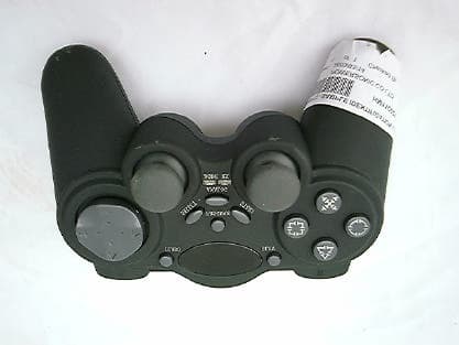
Click to zoom
Application Details
- Equipment Class
- DXT - Part 15 Low Power Transceiver, Rx Verified
- Date of Grant
- May 21, 2003
- Application Purpose
- Original Equipment
- Date of Application
- May 21, 2003
- Equipment Note
- RF Wireless Game Pad
- Frequency Range
- 903.00000000 - 926.60000000
- Company
- POWERSONIC CO., LTD.
- Country
- China
Documents & Files
Document Text
Text extracted from the exhibit documents filed with the FCC. Open a document above to read the original.
External Photos
PHOTOGRAPH OF THE PRODUCT FRONT VIEW OF THE PRODUCT REAR VIEW OF THE PRODUCT
Internal Photos
PHOTOGRAPH OF THE PRODUCT INNER CIRCUIT TOP VIEW INNER CIRCUIT BOTTOM VIEW
Operational Description
Circuit Description 1. Transmitter When receiver received every RF control signal from 902.978MHZ- 903.022MHZ,through the antenna received to module to proceed the buffering and amplifying then send to RF control (EA002HXM) to transform the signals to functional control (ET30X210HXK). The PSII transmitter’s function key signal through the function control IC (ET30X210HXK) transform, sent to RF control IC (EA002HXM) to perform the mix-freq. by using the oscillator 14.7456MHZ.Then send to module to proceed the freq. Rang define and course control after oscillator sent to antenna transmit to receiver. 2. Receiver When transmitter send every RF control signal from 902.978MHZ-903.022MHZ through the antenna received to module to precede the buffering and amplifying then sent to RF control (EA001HXM) to transform the signals to interface control. (EA001HXM) and sent to PSII console. The PSII console sent the protocol through the interface control IC (EA001HXM) transform, sent to RF control IC (EA001HXM) to perform the mix-freq. by using the oscillator 14.7456MHZ.Then sent to module to proceed the freq. Rang define and course control after oscillation sent to antenna transmit to transmitter. 3. Antenna PCB with cupper film, no ground. 4. Power 5(AAA3 rechargeable battery) with 4.5V UL charge. 5. Range 10M
Schematics
22OF PSX RF PAD D2018P-A6.00 SHEET No. SCH. No.REVISION COPYRIGHT 2002 C TITLE: R E V I S I O N S REV.DESIGNEDDATEPCB No.DRAWNCHECKEDCOMMENTSREV. 87654321 D C B A 12345678 A B C D 1 2 3 4 5 6 7 8 9 10 11 12 1314151617181920212223 24 25 26 27 28 29 30 31 32 33 34 35 363738394041424344454647 IC3 ASRF1 R59 24k TR5 8051 1 2 CN5 SIL2 MALE C17 100nF D3 LL4148 RIGHT MTR_0V TR4 8051 1 2 CN4 SIL2 MALE C16 100nF D2 LL4148 MTR_0V SINGLE SHOCK PS2 MOTOR LEFT DUAL SHOCK PS2 MOTOR R37 1k5 0V R36 1k5 0V R47 10k R35 1k5 0V VCC R58 10k R46 1k5 0V VCC R57 10k R45 1k5 0V VCC R56 10k R44 1k5 0V VCC SELECT SW3 0V START SW4 0V R55 10k R43 1k5 0V VCC R54 10k R42 1k5 0V VCC R53 10k R41 1k5 0V VCC R52 10k R40 1k5 0V VCC R39 1k5 0V R38 1k5 0V 0V T3 T2 T1 T5 T4 VCC VCC 0V C15 100nF C8 22uF 0V * OPTIONAL C26 10uF 0V * ESR R60 1R # MTR_VCC1 NOTE: 1) ALL COMPONENTS TO BE SURFACE MOUNT EXCEPT THOSE MARKED WITH AN *. 3) ALL CAPACITORS 6.3V UNLESS OTHERWISE STATED. 2) ALL SURFACE MOUNT COMPONENTS TO BE 0603 EXCEPT THOSE MARKED WITH A $ ARE 0805 AND THOSE MARKED WITH A # ARE 1206. ET30RF900PS2-R 123 CN11 SIL3 123 CN9 SIL3 L3 YL XL R3 YR XR L1L2 VCCVCC R1R2 L2VCCL1R1VCCR2 123456 CN7 SIL6 0V VCC T6 R69 1k R70 1k R71 100k R72 100k 0V0V 1 2 3 4 5 6 CN6 SIL6 RV1C JOYSTICK LEFT RV1B JOYSTICK LEFT XL AXIS YL AXIS 0k(L) <= 5k(C) => 10k(R) 0k(U) <= 5k(C) => 10k(D) RV1A JOYSTICK LEFT L3 JS_VCC JS_VCC JS_0V JS_0V JS_0V RV2C JOYSTICK RIGHT RV2B JOYSTICK RIGHT XR AXIS YR AXIS 0k(L) <= 5k(C) => 10k(R) 0k(U) <= 5k(C) => 10k(D) RV2A JOYSTICK RIGHT R3 JS_VCC JS_VCC JS_0V JS_0V JS_0V JS_VCC JS_0V L3 YL XL R3 YR XR VCC 0V 0.008-02-2002D2018P-A0.0 R74 1R # MTR_VCC2 12 CN13 SIL5 1 2 CN13 SIL5 Schematic Document of Emitter (1) 12OF PSX RF PAD D2018P-A6.00 SHEET No. SCH. No.REVISION COPYRIGHT 2002 C TITLE: R E V I S I O N S REV.DESIGNEDDATEPCB No.DRAWNCHECKEDCOMMENTSREV. 87654321 D C B A 12345678 A B C D ET30RF900PS2-R C18 18pF C19 18pF XL1 14.7456MHz 0V 0V * T4 T3 T2 T1 T5 VCC R14 1k VCC R13 1k TP1 X9 TC PULL TESTPOINT LOW ON BOOT TO INVOKE TEST CODE PULL HIGH IF LED NOT FITTED R23 2k2 VCC X9 VCC 0V C13 100nF C6 22uF 0V VCC 0V 1 2 3 4 5 6 7 8 9 10 11 12 13 14 15 1617 18 19 20 21 22 23 24 25 26 27 28 29 30 31 32 IC1 X9 C12 390pF LK6 LD2 ORANGE RX 0V A B 1 2 3 4 5 6 7 8 9 10 11 12 13 14 15 1617 18 19 20 21 22 23 24 25 26 27 28 29 30 31 32 TR1 8550 R18 5k6 R19 10k R11 1k C9 22nF VCCVCCVCC 0V * CLOSED=CW 0V LK4 R6 47k VCC C4 1uF C1 100pF 0V MOUNT CLOSE TO CN1 R1 1R C11 47uF 0V 0V0V 10V C2 100pF 0V C21 560pF 0V C22 560pF 0V C23 560pF 0V C24 560pF 0V ANT MODULE TANT 1 2 3 4 5 6 7 8 CN2 SIL8 MALE TP2 OUT L1 220nH 1 2 3 4 5 6 CN1 SIL6 MALE 0V TP3 SSI L2 0R 0V C10 SOT DON'T FIT 0V R25330R R26330R R27330R R28330R R10 22k 0V 0V VCC R5 47k VCC R4 47k VCC R3 47k BANK SELECT OPEN = A CLOSED = B R8 4k7 BNK_SEL CH2 CH3 CH4 R7 4k7 VCC R2 47k CLOSED=LP LK2 OPEN=HP C5 47uF * 10V TP4 ANTENNA WIRE R29 0R TP5 R30 0R ANTENNA PRINTED DON'T FIT R33 3R3 1 2 3 45 6 7 8 SW1 4 WAY DIP DON'T CLOSE LK3 XBox close R12 1k R16 1k 0V VCC TR3 8050 0V R9 4k7 R21 100k 0V R15 1k TR2 8550 R20 100k BATT D1 LL4148 BATT 0V R24 2k2 NOTE: 1) ALL COMPONENTS TO BE SURFACE MOUNT EXCEPT THOSE MARKED WITH AN *. 3) ALL CAPACITORS 6.3V UNLESS OTHERWISE STATED. 2) ALL SURFACE MOUNT COMPONENTS TO BE 0603 EXCEPT THOSE MARKED WITH A $ ARE 0805 AND THOSE MARKED WITH A # ARE 1206. 1 2 CN3 SIL2 MALE BATTERIES 2xAAA 3V 0VMTR_0V BATT R22 1k T6 R31 1k DON'T FIT=USA FIT=EUROPE DON'T FIT VCC $ MTR_VCC1 DON'T FIT OR 10uF LOW ESR 10V TANT TANT RUMBLE DISABLE R73 47k VCC CLOSE TO XL1 0.008-02-2002D2018P-A0.0 MTR_VCC2 DON'T FIT LD1 GREEN Mode VCC SW2 SW-PB BATT MD_SW Schematic Document of Emitter (2) 1234 A B C D 4 321 D C B A Title NumberRevisionSize A4 Date:19-Apr-2002Sheet of File:C:\Documents and Settings\Administrator\ \Sheet1.DDBDrawn By: 1 2 3 4 5 6 78 9 10 11 12 13 14 DIP-14 LM324 R8 100 R6 30K R5 470K D6 LED R1 1.5 R7 2K D3 IN4001 D2 IN4148 D1IN4148 C3104 C2 104 C1 47uF R3 330K R4 51K D5 LED R9 100 VCC BATT+ BATT- R2 1K D4 LED Schematic Document of Charger
Test Report
Alice, Technical review of the referenced application has been performed. Please provide responses to the questions listed below, so that review of the application may be completed and a grant issued. Thank you. Gregory Czumak EMC Consultant MET Labs RT Questions: 1. What is the actual tuning range of the EUT, lowest channel to highest channel? 2. Radiated emission data for the second harmonic of the fundamental emission has been provided. What detector function was used to make these measurements? Peak? Average? What RBW and VBW? 3. The table of radiated emissions on page 19 of 27 of the test report is illegible. Please provide another copy of the table. 4. Please provide spectral plots of the fundamental emission tuned to both the lowest and highest channel, in order to demonstrate compliance with the bandedge requirement of Section 15.249(d).
Test Report
Bandedge Measurement (Section 15.249(d))Bandedge Measurement (Section 15.249(d)) Lowest Frequency: Highest Frequency:Highest Frequency:
Test Setup Photos
TEST SET UP PHOTOGRAPH OF THE PRODUCT MEASUREMENT OF RADIATED EMISSION TEST SET UP MEASUREMENT OF CONDUCTED EMISSION TEST SET UP
Contact Information
Applicant
Ranke Joe(General Manager)
Technical Contact
MET Laboratories Inc.Chris Harvey
410-354-3300
914 W. Patapsco Avenue · Baltimore, Maryland · United States
Test Firm
Hong Kong Standards & Testing Cen.Wilson Wong
Technical Specifications
| # | Rule Parts | Frequency Range | Power Output |
|---|---|---|---|
| 1 | 15C | 903 MHz - 926.6 MHz | - |