Q8KPCSHW70ABi-directional booster
G-Way Solutions, LLC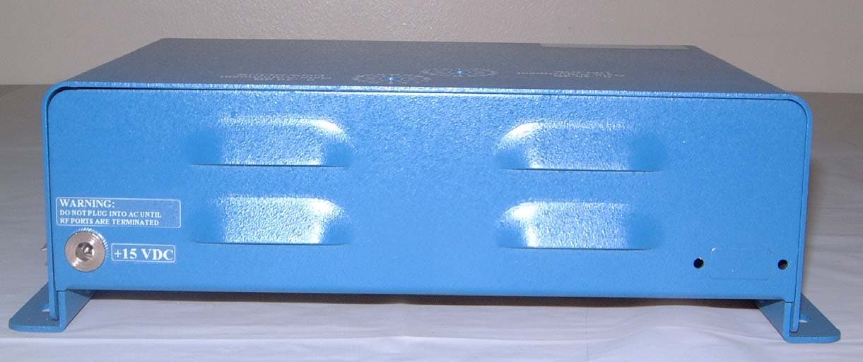
Click to zoom
Application Details
- Equipment Class
- PCB - PCS Licensed Transmitter
- Date of Grant
- Jun 28, 2004
- Application Purpose
- Original Equipment
- Date of Application
- Jun 28, 2004
- Equipment Note
- Bi-directional booster
- Frequency Range
- 1930.00000000 - 1990.00000000
- Company
- G-Way Solutions, LLC
- Country
- United States
Documents & Files
Document Text
Text extracted from the exhibit documents filed with the FCC. Open a document above to read the original.
Users Manual
INSTALLATION AND OPERATING MANUAL FOR BDA-1XXX-.X/.XW-XX-AX MINI-BI-Directional Amplifier TABLE OF CONTENTS PARAGRAPH PAGE NO Mini-BDA OVERVIEW 3 Mini-BDA BLOCK DIAGRAM DESCRIPTION 3 Mini-BDA OPTIONS 3 Mini-BDA BLOCK DIAGRAM DRAWING (Figure 1) 4 ELECTRICAL SPECIFICATIONS 5 FREQUENCY RANGES (Table 1) 6 SYSTEM SPECIFICATIONS (Table 2) 6 MECHANICAL CONNECTIONS 7 ENVIRONMENTAL CONDITIONS 7 Mini-BDA CONNECTIONS 7 MECHANICAL OUTLINE DRAWING (Figure 3 & 3a)8 RF EXPOSURE WARNING 9 Mini-BDA INSTALLATION 10 Mini-BDA OPERATION 11 MECHANICAL OUTLINE- ADJUSTMENT (Figure 4) 12 DIAGNOSTICS GUIDE 13 Page 2 Mini-BDA OVERVIEW: The Mini-BDA assembly extends the coverage area of radio communications in buildings and RF shielded environments. The Mini-BDA has dual RF paths to extend coverage in two distinct frequency bands. The unit features low noise figure and wide dynamic range. It is based on a duplexed path configuration with sharp out of band attenuation allowing improved isolation between the receiving and transmitting paths. Mini-BDA BLOCK DIAGRAM DESCRIPTION: Refer to Figure 1 for the following discussion. The Mini-BDA Downlink path receives RF signals from the base station and amplifies and transmits them to the subscriber. The Mini-BDA Uplink path receives RF signals from the subscriber and amplifies and transmits them to the base station. The Uplink and Downlink occupy two distinct frequency bands. For example, the PCS A frequency bands are as follows: 1850-1865 MHz for the Uplink and 1930-1945 MHz for the Downlink. Two diplexers isolate the paths and route each signal to the proper amplifying channel. An Automatic Level Control (ALC) allows for output power limiting. A variable step attenuator gives 0 – 30 dB of attenuation in 2 dB steps. The use of these controls is covered in the “OPERATION” section, later in this document. Mini-BDA Options: The Mini-BDA can be used as a line amplifier. With an optional external bias-tee, the Mini-BDA will function with power coming from the In-building antenna. Optional External Bias-Tees (For .1/.1 Watt Models only) An optional 9 pin D-sub connector is available for external alarm monitoring (See Figures 3 & 3a). Page 3 Figure 1 1. 2. 3. 4. 5. 6. Mini-BDA BLOCK DIAGRAM 1. Up-Link Diplexer - has low pass band insertion loss and high selectivity 2. Down-Link Pre-amp - is a low noise amplifier that drives the Down-Link MPA and offers 38dB Gain 3. Down-Link MPA – is a medium power amplifier with an ALC circuit which offers 40dB Gain. (High power amplifier with an ALC circuit which offers 40dB Gain for 1 & 2 Watt models) 4. Up-Link MPA – is a medium power amplifier with an ALC circuit which offers 40dB Gain 5. Up-Link Pre-amp - is a low noise amplifier that drives the Up-Link MPA and offers 38dB Gain 6. Down-Link Diplexer - has low pass band insertion loss and high selectivity Page 4 ELECTRICAL SPECIFICATIONS: Frequency Range : See Table 1 Pass band Gain @ min attenuation : See Table 2 Nominal Channel Bandwidth : 25.3 MHz typical Variable Step Attenuator Range : 0-30 dB (2-dB steps) Pass band Ripple : ±1.5 dB typical Noise Figure @+25 °C at max gain : 3.0 dB max. 3rd Order Intercept point : See Table 2 Output Power @ 1dB Compression : See Table 2 Isolation between Up/Down Link : 80 dB min., 90 typical Input/ Output Impedance : 50 Ohms VSWR (Input/Output) : 1.5: 1 max Power Supply (Local) : 15VDC/1.67 Amp : (24VDC/1.88 Amp for 1 Watt Model) : (24VDC/3 Amp for 2 Watt Model) Page 5 Table 1 Frequency Band Downlink Frequency Ranges Uplink Frequency Ranges PCS A 1930-1945 MHz 1850-1865 MHz PCS B 1950-1965 MHz 1870-1885 MHz PCS C 1975-1990 MHz 1895-1910 MHz PCS D 1945-1950 MHz 1865-1870 MHz PCS E 1965-1970 MHz 1885-1890 MHz PCS F 1970-1975 MHz 1890-1895 MHz Table 2 System Pass band Gain (dB) Typ. 3rd Order Intercept Point (dBm) Typ. Output Power @ 1dB Compression (dBm) Typ. ALC Factory Set Point (dBm) Uplink Downlink Uplink Downlink Uplink Downlink Uplink Downlink .1/.1 Watt 70 dB Gain 72 72 33 33 19 19 10 10 .1/.5 Watt 70 dB Gain 72 72 33 39 19 26 10 18 .5/.5 Watt 70 dB Gain 72 72 39 39 27 26 18 18 .5 / 1 Watt 70 dB Gain 72 72 39 44 27 31 18 22 .5 / 2 Watt 70 dB Gain 72 72 39 46 27 36 18 27 .1/.1 Watt 60 dB Gain 61 61 34 34 20 20 11 11 .1/.5 Watt 60 dB Gain 61 61 34 40 20 27 11 18 .5/.5 Watt 60 dB Gain 61 61 40 40 27 27 18 18 .5 / 1 Watt 60 dB Gain 61 61 39 44 27 31 18 22 .5 / 2 Watt 60 dB Gain 61 61 39 46 27 36 18 27 The Manufacturer's rated output power of this equipment is for single carrier operation. For situations when multiple carrier signals are present, the rating would have to be reduced by 3.5 dB, especially where the output signal is re-radiated and can cause interference to adjacent band users. This power reduction is to be by means of input power or gain reduction and not by an attenuator at the output of the device. Page 6 MECHANICAL SPECIFICATIONS: Size : 8.75 x 6.20 x 3.0 inch : (222.3 x 157.5 x 76.2 mm) RF Connectors : N-type Female Weight : 2.0 Lbs. (4.4 kg.) approx. ENVIRONMENTAL CONDITIONS: The unit is designed for indoor applications: Operating temperature: - 20°C to + 50°C Storage temperature: - 50°C to + 90°C Mini-BDA CONNECTIONS The Mini-BDA is powered by a +15 VDC/1.67 Amp Wall Plug-In AC adapter with a 2.5 mm output connector (+24 VDC/1.88 Amp Desk Top AC adapter for 1 Watt models and (+24 VDC/3.0 Amp Desk Top AC adapter for 2 Watt models). The Wall Plug-In and Desk Top power adapters are highly reliable and compact, designed for use in telecommunications. The power adapters are CE & UL approved. The metal enclosure of the Mini-BDA is connected to ground. A 9-pin D-Sub connector provides failure alarm output contacts. The RF connections are made via two type “N” female connectors. The RF connector labeled “BASE” must be connected to the antenna pointing towards the base station. The RF connection labeled “MOBILE” must be connected to the antenna facing the area to be covered by the Mini-BDA. The RF connections must be made through cables with…
Text truncated - open the document above for the full version.
Cover Letter(s)
G-Wave Incorporated 15 Ron’s Edge Road Springfield, NJ 07081 Tel 201-343-3140 Fax 201-343-6390 E-mail [email protected] Website: www.gwaverf.com April 15, 2004 Federal Communications Commission Office of Engineering and Technology 7435 Oakland Mills Rd. Columbia, MD 21046 Subject: Request for Confidentiality Dear Sir or Madam: G-Wave Incorporated respectfully requests that the schematic diagrams, block diagram, and circuit descriptions submitted with the application for certification under FCC ID Q8KPCSHW70A be withheld from public disclosure. This request is made under the provisions of Section 0.457 (d) of the Commission’s rules and Section 0.552 (b) (4) of the Freedom of Information Act. This product has been developed at considerable expense, and disclosure of this information would place G- Wave Incorporated at a competitive disadvantage. Thank you for your attention to this matter. Sincerely yours, G-Wave Incorporated Greg David Sr. Technical Consultant 15 Ron's Edge Road Springfield, NJ 07081 Tel: (201) 343-3140 Fax: (201) 343-6390 www.gwaverf.com
Cover Letter(s)
G-Wave Incorporated 15 Ron’s Edge Road Springfield, NJ 07081 Tel 201-343-3140 Fax 201-343-6390 E-mail [email protected] Website: www.gwaverf.com April 12, 2004 G-Wave Incorporated respectfully states that all models for certification under FCC ID Q8KPCSHW70A and Industry Canada ID 4901A-PCSHW70A are identical except for different diplexers which allow for the distinct frequency band blocks. Sincerely yours, G-Wave Incorporated Greg David Sr. Technical Consultant 15 Ron's Edge Road Springfield, NJ 07081 Tel: (201) 343-3140 Fax: (201) 343-6390 www.gwaverf.com
Cover Letter(s)
G-Wave Incorporated 15 Ron’s Edge Road Springfield, NJ 07081 Tel 201-343-3140 Fax 201-343-6390 E-mail [email protected] Website: www.gwaverf.com DATE Nemko Canada Inc 303 River Road Ottawa, Ontario, Canada K1V 1H2 Attn: Director of Certification Authority to Act as Agent On our behalf, I appoint Nemko Canada Inc. 303 River Road Ottawa, Ontario, Canada K1V 1H2, to act as our agent in the preparation of this application for equipment certification. I certify that submitted documents properly describe the device or system for which equipment certification is sought. I also certify that each unit manufactured, imported or marketed, as defined in the Federal Communications Commission’s regulations will have affixed to it a label identical to that submitted for approval with this application. For instances where our authorized agent signs the application for certification on our behalf, I acknowledge that all responsibility for complying with the terms and conditions for certification, as specified by Nemko Canada Inc, still resides with G-Wave Inc. 15 Ron’s Edge Road, Springfield, New Jersey 07081. Dated this 23rd Day of June 20 04 Agency agreement expiration date: Usually Give 8 - 12 Months By: Greg David Signature Printed Title: Sr. Technical Consultant On behalf of : G-Wave Inc. Telephone: 201-343-3140 15 Ron's Edge Road Springfield, NJ 07081 Tel: (201) 343-3140 Fax: (201) 343-6390 www.gwaverf.com
Internal Photos
PCB Back (same PCB’s for uplink and downlink) MA1XXX/1.0/XXSK-A1 MA1XXX/1.0/75SK-A2-2 PCB Front final assembl y (same assemblies for uplink and downlink)
Parts List/Tune Up Info
FCC ID: Q8KPCSHW70A RF OUTPUT STAGE BIASING IN BDA-PCS/A-0.5/0.5W-70 BDA. Uplink: Output stage: Sirenza Microdevices SHF-0289 D.C. bias: Vdd= +8.0 Volts, Vgg= -1.0 Volt @ 220 mA, typ. Downlink: Output stage: Sirenza Microdevices SHF-0289 D.C. bias: Vdd= +8.0 Volts, Vgg= -1.0 Volt @ 220 mA, typ. Page 1
Parts List/Tune Up Info
FCC ID: Q8KPCSHW70A RF OUTPUT STAGE BIASING IN BDA-PCS/B-0.5/0.5W-70 BDA. Uplink: Output stage: Sirenza Microdevices SHF-0289 D.C. bias: Vdd= +8.0 Volts, Vgg= -1.0 Volt @ 220 mA, typ. Downlink: Output stage: Sirenza Microdevices SHF-0289 D.C. bias: Vdd= +8.0 Volts, Vgg= -1.0 Volt @ 220 mA, typ. Page 1
Parts List/Tune Up Info
FCC ID: Q8KPCSHW70A RF OUTPUT STAGE BIASING IN BDA-PCS/C-0.5/0.5W-70 BDA. Uplink: Output stage: Sirenza Microdevices SHF-0289 D.C. bias: Vdd= +8.0 Volts, Vgg= -1.0 Volt @ 220 mA, typ. Downlink: Output stage: Sirenza Microdevices SHF-0289 D.C. bias: Vdd= +8.0 Volts, Vgg= -1.0 Volt @ 220 mA, typ. Page 1
Parts List/Tune Up Info
FCC ID: Q8KPCSHW70A RF OUTPUT STAGE BIASING IN BDA-PCS/D-0.5/0.5W-70 BDA. Uplink: Output stage: Sirenza Microdevices SHF-0289 D.C. bias: Vdd= +8.0 Volts, Vgg= -1.0 Volt @ 220 mA, typ. Downlink: Output stage: Sirenza Microdevices SHF-0289 D.C. bias: Vdd= +8.0 Volts, Vgg= -1.0 Volt @ 220 mA, typ. Page 1
Parts List/Tune Up Info
FCC ID: Q8KPCSHW70A RF OUTPUT STAGE BIASING IN BDA-PCS/E-0.5/0.5W-70 BDA. Uplink: Output stage: Sirenza Microdevices SHF-0289 D.C. bias: Vdd= +8.0 Volts, Vgg= -1.0 Volt @ 220 mA, typ. Downlink: Output stage: Sirenza Microdevices SHF-0289 D.C. bias: Vdd= +8.0 Volts, Vgg= -1.0 Volt @ 220 mA, typ. Page 1
Parts List/Tune Up Info
FCC ID: Q8KPCSHW70A RF OUTPUT STAGE BIASING IN BDA-PCS/F-0.5/0.5W-70 BDA. Uplink: Output stage: Sirenza Microdevices SHF-0289 D.C. bias: Vdd= +8.0 Volts, Vgg= -1.0 Volt @ 220 mA, typ. Downlink: Output stage: Sirenza Microdevices SHF-0289 D.C. bias: Vdd= +8.0 Volts, Vgg= -1.0 Volt @ 220 mA, typ. Page 1
Parts List/Tune Up Info
ALC (Automatic Level Control) To minimize intermodulation products, each amplifier in the BDA contains an ALC feedback loop. The ALC circuit senses the output power and limits it to the factory preset level. ALC function is selected with an on/off toggle switch located on each amplifier and accessible by removing of the BDA enclosures top cover. Both red indicator lamps are located on the front panel of the BDA and illuminate when output power exceeds the ALC set point. The indicator is functional regardless of the position of the ALC switch. To increase or decrease the output power, remove the top cover (See picture below) to make the adjustment. The adjustment has to be made with the output power 3-4 dB above the ALC setting (3-4dB after the ALC LED is illuminated) and the ALC switch has to be in the on position. Both uplink and downlink adjustments have a tamper sticker covering it, remove them for adjustment. Adjust output power level to desired value by varying the uplink or downlink ALC adjustment. NOTE: Output power level is recommended set at 7 dB below the amplifier P1dB measurement (see specification sheet) to minimize intermodulation products. Downlink ALC Switch Uplink ALC Switch Downlink ALC Adjustment Uplink ALC Adjustment O N O FF OFF ON 15 Ron's Edge Road Springfield, NJ 07081 Tel: (201) 343-3140 Fax: (201) 343-6390 www.gwaverf.com
RF Exposure Info
Maximum Permissible Exposure (MPE) Compliance BDA-PCS/A-0.5/0.5W-70-A FCC ID Q8KPCSHW70A At the maximum operating frequency of 1945MHz (Downlink) and 1865MHz (Uplink) the MPE limit for the General Population/Uncontrolled Exposure is as follows: Downlink = 1.0mW/cm2 and Uplink = 1.0mW/cm2. The analysis is provided below. Power Density (S) = EIRP/(4πR²), Therefore, R≥√EIRP/S x 4π From the above calculations, with: Downlink Maximum Antenna Gain = 2dBi Uplink Maximum Antenna Gain = 11dBi Downlink Maximum output power = 18dBm Uplink Maximum output power = 18dBm S = 1.0 mW/cm2 S = 1.0 mW/cm2 EIRP = 20dBm or .10W (worst case) EIRP = 29dBm or .794W (worst case) Therefore, R= 2.82cm (Downlink) R= 7.95cm (Uplink) These are the minimum safe distances for the general population for each antenna.
RF Exposure Info
Maximum Permissible Exposure (MPE) Compliance BDA-PCS/B-0.5/0.5W-70-A FCC ID Q8KPCSHW70A At the maximum operating frequency of 1965MHz (Downlink) and 1885MHz (Uplink) the MPE limit for the General Population/Uncontrolled Exposure is as follows: Downlink = 1.0mW/cm2 and Uplink = 1.0mW/cm2. The analysis is provided below. Power Density (S) = EIRP/(4πR²), Therefore, R≥√EIRP/S x 4π From the above calculations, with: Downlink Maximum Antenna Gain = 2dBi Uplink Maximum Antenna Gain = 11dBi Downlink Maximum output power = 18dBm Uplink Maximum output power = 18dBm S = 1.0 mW/cm2 S = 1.0 mW/cm2 EIRP = 20dBm or .10W (worst case) EIRP = 29dBm or .794W (worst case) Therefore, R= 2.82cm (Downlink) R= 7.95cm (Uplink) These are the minimum safe distances for the general population for each antenna.
RF Exposure Info
Maximum Permissible Exposure (MPE) Compliance BDA-PCS/C-0.5/0.5W-70-A FCC ID Q8KPCSHW70A At the maximum operating frequency of 1990MHz (Downlink) and 1910MHz (Uplink) the MPE limit for the General Population/Uncontrolled Exposure is as follows: Downlink = 1.0mW/cm2 and Uplink = 1.0mW/cm2. The analysis is provided below. Power Density (S) = EIRP/(4πR²), Therefore, R≥√EIRP/S x 4π From the above calculations, with: Downlink Maximum Antenna Gain = 2dBi Uplink Maximum Antenna Gain = 11dBi Downlink Maximum output power = 18dBm Uplink Maximum output power = 18dBm S = 1.0 mW/cm2 S = 1.0 mW/cm2 EIRP = 20dBm or .10W (worst case) EIRP = 29dBm or .794W (worst case) Therefore, R= 2.82cm (Downlink) R= 7.95cm (Uplink) These are the minimum safe distances for the general population for each antenna.
RF Exposure Info
Maximum Permissible Exposure (MPE) Compliance BDA-PCS/D-0.5/0.5W-70-A FCC ID Q8KPCSHW70A At the maximum operating frequency of 1950MHz (Downlink) and 1870MHz (Uplink) the MPE limit for the General Population/Uncontrolled Exposure is as follows: Downlink = 1.0mW/cm2 and Uplink = 1.0mW/cm2. The analysis is provided below. Power Density (S) = EIRP/(4πR²), Therefore, R≥√EIRP/S x 4π From the above calculations, with: Downlink Maximum Antenna Gain = 2dBi Uplink Maximum Antenna Gain = 11dBi Downlink Maximum output power = 18dBm Uplink Maximum output power = 18dBm S = 1.0 mW/cm2 S = 1.0 mW/cm2 EIRP = 20dBm or .10W (worst case) EIRP = 29dBm or .794W (worst case) Therefore, R= 2.82cm (Downlink) R= 7.95cm (Uplink) These are the minimum safe distances for the general population for each antenna.
RF Exposure Info
Maximum Permissible Exposure (MPE) Compliance BDA-PCS/E-0.5/0.5W-70-A FCC ID Q8KPCSHW70A At the maximum operating frequency of 1970MHz (Downlink) and 1890MHz (Uplink) the MPE limit for the General Population/Uncontrolled Exposure is as follows: Downlink = 1.0mW/cm2 and Uplink = 1.0mW/cm2. The analysis is provided below. Power Density (S) = EIRP/(4πR²), Therefore, R≥√EIRP/S x 4π From the above calculations, with: Downlink Maximum Antenna Gain = 2dBi Uplink Maximum Antenna Gain = 11dBi Downlink Maximum output power = 18dBm Uplink Maximum output power = 18dBm S = 1.0 mW/cm2 S = 1.0 mW/cm2 EIRP = 20dBm or .10W (worst case) EIRP = 29dBm or .794W (worst case) Therefore, R= 2.82cm (Downlink) R= 7.95cm (Uplink) These are the minimum safe distances for the general population for each antenna.
RF Exposure Info
Maximum Permissible Exposure (MPE) Compliance BDA-PCS/F-0.5/0.5W-70-A FCC ID Q8KPCSHW70A At the maximum operating frequency of 1975MHz (Downlink) and 1895MHz (Uplink) the MPE limit for the General Population/Uncontrolled Exposure is as follows: Downlink = 1.0mW/cm2 and Uplink = 1.0mW/cm2. The analysis is provided below. Power Density (S) = EIRP/(4πR²), Therefore, R≥√EIRP/S x 4π From the above calculations, with: Downlink Maximum Antenna Gain = 2dBi Uplink Maximum Antenna Gain = 11dBi Downlink Maximum output power = 18dBm Uplink Maximum output power = 18dBm S = 1.0 mW/cm2 S = 1.0 mW/cm2 EIRP = 20dBm or .10W (worst case) EIRP = 29dBm or .794W (worst case) Therefore, R= 2.82cm (Downlink) R= 7.95cm (Uplink) These are the minimum safe distances for the general population for each antenna.
Test Report
Master: FCC-PR24-E Date: February 13, 2002 Test Report: 4W08096 Applicant: G-Wave Inc. 15 Ron’s Edge Road Springfield, NJ, USA 07081 Equipment Under Test: BDA-PCS/A-0.5/0.5W-70-A (EUT) BDA-PCS/B-0.5/0.5W-70-A BDA-PCS/C-0.5/0.5W-70-A BDA-PCS/D-0.5/0.5W-70-A BDA-PCS/E-0.5/0.5W-70-A BDA-PCS/F-0.5/0.5W-70-A Q8KPCSHW70A FCC ID: In Accordance With: FCC Part 24, Subpart E Tested By: Nemko Canada Inc. 303 River Road, R.R. 5 Ottawa, Ontario K1V 1H2 Authorized By: Glen Westwell, Wireless Technologist Date: 22 June 2004 Total Number of Pages: 39 Nemko Canada Inc. FCC PART 24, SUBPART E PROJECT NO.:4W08096 EQUIPMENT: BDA-PCS/A-0.5/0.5W-70-A, BDA-PCS/B-0.5/0.5W-70-A, BDA-PCS/C-0.5/0.5W-70-A BDA-PCS/D-0.5/0.5W-70-A, BDA-PCS/E-0.5/0.5W-70-A, BDA-PCS/F-0.5/0.5W-70-A Page 2 of 39 Table of Contents Section 1. Summary of Test Results .................................................................................. 3 Section 2. General Equipment Specification..................................................................... 5 Section 3. RF Power Output ............................................................................................... 7 Section 4. Occupied Bandwidth ......................................................................................... 8 Section 5. Spurious Emissions at Antenna Terminals ................................................... 12 Section 6. Field Strength of Spurious .............................................................................. 33 Section 7. Block Diagrams ................................................................................................ 36 Section 8. Test Equipment List ........................................................................................ 39 Nemko Canada Inc. FCC PART 24, SUBPART E PROJECT NO.:4W08096 EQUIPMENT: BDA-PCS/A-0.5/0.5W-70-A, BDA-PCS/B-0.5/0.5W-70-A, BDA-PCS/C-0.5/0.5W-70-A BDA-PCS/D-0.5/0.5W-70-A, BDA-PCS/E-0.5/0.5W-70-A, BDA-PCS/F-0.5/0.5W-70-A Page 3 of 39 Section 1. Summary of Test Results General All measurements are traceable to national standards. These tests were conducted on a sample of the equipment for the purpose of demonstrating compliance with FCC Part 24, Subpart E. THIS TEST REPORT RELATES ONLY TO THE ITEM(S) TESTED. THE FOLLOWING DEVIATIONS FROM, ADDITIONS TO, OR EXCLUSIONS FROM THE TEST SPECIFICATIONS HAVE BEEN MADE. See “ Summary of Test Data”. TESTED BY: ______________________________ DATE: June 18, 2004 Daxesh Thakker, Wireless Test Engineer TESTED BY: ______________________________ DATE: June 18, 2004 Kevin Carr, EMC/EMI/Wireless Specialist Nemko Canada Inc. authorizes the above named company to reproduce this report provided it is reproduced in its entirety and for use by the company’s employees only. Any use which a third party makes of this report, or any reliance on or decisions to be made based on it, are the responsibility of such third parties. Nemko Canada Inc. accepts no responsibility for damages, if any, suffered by any third party as a result of decisions made or actions based on this report. This report applies only to the items tested. Nemko Canada Inc. FCC PART 24, SUBPART E PROJECT NO.:4W08096 EQUIPMENT: BDA-PCS/A-0.5/0.5W-70-A, BDA-PCS/B-0.5/0.5W-70-A, BDA-PCS/C-0.5/0.5W-70-A BDA-PCS/D-0.5/0.5W-70-A, BDA-PCS/E-0.5/0.5W-70-A, BDA-PCS/F-0.5/0.5W-70-A Page 4 of 39 Summary Of Test Data Name Of Test Para. No. Result RF Power Output 2.1046 Complied Occupied Bandwidth 2.1049 Complied Spurious Emissions at Antenna Terminals 2.1051 Complied Field Strength of Spurious Emissions 2.1053 Complied Frequency Stability 2.1055 N/A, the Eut is not a band translator Test Conditions: - The EUT was tested at full power - Testing was performed at proper temperature and humidity - At the clients request, testing was conducted on downlink side only, due to changes in the downlink amplifier. The uplink data should be used from Nemko project 07892, appropriate report page references have been made through out the report - Testing was carried out on the top, middle and bottom PCS Bands only. - The device employs a ALC, and was assessed at max. I/P Power as per published gain levels - Radiated testing was done on the top mid and bottom freq’s of the PCS Band Indoor Temperature: 24 °C Humidity: 45% Nemko Canada Inc. FCC PART 24, SUBPART E PROJECT NO.:4W08096 EQUIPMENT: BDA-PCS/A-0.5/0.5W-70-A, BDA-PCS/B-0.5/0.5W-70-A, BDA-PCS/C-0.5/0.5W-70-A BDA-PCS/D-0.5/0.5W-70-A, BDA-PCS/E-0.5/0.5W-70-A, BDA-PCS/F-0.5/0.5W-70-A Page 5 of 39 Section 2. General Equipment Specification Manufacturer: G-Wave Inc. Model No./Serial No. Submitted for Assessment: BDA-PCS/A-0.5/0.5W-70-A, 04021001 BDA-PCS/B-0.5/0.5W-70-A, 04021001 BDA-PCS/C-0.5/0.5W-70-A, 04021001 Date Received In Laboratory: 3 June 2004 Nemko Identification No.: 1, 2, 3 Supply Voltage: 120VAC, 60Hz Frequency Range: Downlink: 1930 – 1990 MHz RF Output Power (Rated) Downlink: 18.0dBm, Total composite Power, 2 Tone RF Output Power (measured) Downlink: 18.0dBm, Total composite Power, 2 Tone Emission Designator: DXW, F9W, GXW NOTE: UL data can be found on page 5, in report 4W07892, Issue 2 included in the submission package Nemko Canada Inc. FCC PART 24, SUBPART E PROJECT NO.:4W08096 EQUIPMENT: BDA-PCS/A-0.5/0.5W-70-A, BDA-PCS/B-0.5/0.5W-70-A, BDA-PCS/C-0.5/0.5W-70-A BDA-PCS/D-0.5/0.5W-70-A, BDA-PCS/E-0.5/0.5W-70-A, BDA-PCS/F-0.5/0.5W-70-A Page 6 of 39 Block Diagram: DL I/P UL I/P EUT AC/DC Converter CINCON ELECTRONICS AC ADAPTER M/N TR25150 S/N 25150-0001043 120VAC, 60Hz Nemko Canada Inc. FCC PART 24, SUBPART E PROJECT NO.:4W08096 EQUIPMENT: BDA-PCS/A-0.5/0.5W-70-A, BDA-PCS/B-0.5/0.5W-70-A, BDA-PCS/C-0.5/0.5W-70-A BDA-PCS/D-0.5/0.5W-70-A, BDA-PCS/E-0.5/0.5W-70-A, BDA-PCS/F-0.5/0.5W-70-A Page 7 of 39 Section 3. RF Power Output Para. No.: 2.1046 Test Performed By: Kevin Carr Date of Test: 10 June 04 Minimum Standard: Para. No.: 24.232. Test Results: Complied, UL data can be found on page 7, in report 4W07892, Issue 2 included in the submission package …
Text truncated - open the document above for the full version.
Test Report
First Diplexer’s Isolation and Rejection Frequency Response Second Diplexer’s Isolation and Rejection Frequency Response Frequency Response Combination of both Diplexers
Test Report
First Diplexer’s Isolation and Rejection Frequency Response Second Diplexer’s Isolation and Rejection Frequency Response Frequency Response Combination of both Diplexers
Test Report
First Diplexer’s Isolation and Rejection Frequency Response Second Diplexer’s Isolation and Rejection Frequency Response Frequency Response Combination of both Diplexers
Test Report
Master: FCC-PR24-E Date: February 13, 2002 Test Report: 4W07892, ISSUE 2 Applicant: G-Wave Inc. 15 Ron’s Edge Road Springfield, NJ 07081 Equipment Under Test: BDA-PCS/A-.5/2W-70-A, BDA-PCS/B-.5/2W-70-A, (EUT) BDA-PCS/C-.5/2W-70-A, BDA-PCS/D-.5/2W-70-A, BDA-PCS/E-.5/2W-70-A, BDA-PCS/F-.5/2W-70-A FCC ID: Q8KPCS2W70A In Accordance With: FCC Part 24, Subpart E Tested By: Nemko Canada Inc. 303 River Road, R.R. 5 Ottawa, Ontario K1V 1H2 Authorized By: Glen Westwell, Wireless Specialist Date: 12 March 2004 Total Number of Pages: 40 Nemko Canada Inc. FCC PART 24, SUBPART E PROJECT NO.:4W07892, ISSUE 2 EQUIPMENT: BDA-PCS/A-.5/2W-70-A, BDA-PCS/B-.5/2W-70-A, BDA-PCS/C-.5/2W-70-A, BDA-PCS/D-.5/2W-70-A, BDA-PCS/E-.5/2W-70-A, BDA-PCS/F-.5/2W-70-A Page 2 of 40 Table of Contents Section 1. Summary of Test Results .................................................................................. 3 Section 2. General Equipment Specification..................................................................... 5 Section 3. RF Power Output ............................................................................................... 7 Section 4. Occupied Bandwidth ......................................................................................... 8 Section 5. Spurious Emissions at Antenna Terminals ................................................... 15 Section 6. Field Strength of Spurious .............................................................................. 34 Section 7. Block Diagrams ................................................................................................ 37 Section 8. Test Equipment List ........................................................................................ 40 Nemko Canada Inc. FCC PART 24, SUBPART E PROJECT NO.:4W07892, ISSUE 2 EQUIPMENT: BDA-PCS/A-.5/2W-70-A, BDA-PCS/B-.5/2W-70-A, BDA-PCS/C-.5/2W-70-A, BDA-PCS/D-.5/2W-70-A, BDA-PCS/E-.5/2W-70-A, BDA-PCS/F-.5/2W-70-A Page 3 of 40 Section 1. Summary of Test Results General All measurements are traceable to national standards. These tests were conducted on a sample of the equipment for the purpose of demonstrating compliance with FCC Part 24, Subpart E. THIS TEST REPORT RELATES ONLY TO THE ITEM(S) TESTED. THE FOLLOWING DEVIATIONS FROM, ADDITIONS TO, OR EXCLUSIONS FROM THE TEST SPECIFICATIONS HAVE BEEN MADE. NONE See “ Summary of Test Data”. TESTED BY: ______________________________ DATE: 12 March 2004 Kevin Carr, EMC/EMI/Wireless Specialist Nemko Canada Inc. authorizes the above named company to reproduce this report provided it is reproduced in its entirety and for use by the company’s employees only. Any use which a third party makes of this report, or any reliance on or decisions to be made based on it, are the responsibility of such third parties. Nemko Canada Inc. accepts no responsibility for damages, if any, suffered by any third party as a result of decisions made or actions based on this report. This report applies only to the items tested. Nemko Canada Inc. FCC PART 24, SUBPART E PROJECT NO.:4W07892, ISSUE 2 EQUIPMENT: BDA-PCS/A-.5/2W-70-A, BDA-PCS/B-.5/2W-70-A, BDA-PCS/C-.5/2W-70-A, BDA-PCS/D-.5/2W-70-A, BDA-PCS/E-.5/2W-70-A, BDA-PCS/F-.5/2W-70-A Page 4 of 40 Summary Of Test Data Name Of Test Para. No. Result RF Power Output 2.1046 Complied Occupied Bandwidth 2.1049 Complied Spurious Emissions at Antenna Terminals 2.1051 Complied Field Strength of Spurious Emissions 2.1053 Complied Frequency Stability 2.1055 N/A(1) Footnotes For N/A’s: N/A(1) – The EUT is a F1 – F1 BDA Test Conditions: Indoor Temperature: 24°C Humidity: 13% Outdoor Temperature: 3°C Humidity: 93% Nemko Canada Inc. FCC PART 24, SUBPART E PROJECT NO.:4W07892, ISSUE 2 EQUIPMENT: BDA-PCS/A-.5/2W-70-A, BDA-PCS/B-.5/2W-70-A, BDA-PCS/C-.5/2W-70-A, BDA-PCS/D-.5/2W-70-A, BDA-PCS/E-.5/2W-70-A, BDA-PCS/F-.5/2W-70-A Page 5 of 40 Section 2. General Equipment Specification Manufacturer: G-Wave Inc. Model No.‘s Tested: BDA-PCS/A-.5/2W-70-A BDA-PCS/B-.5/2W-70-A BDA-PCS/C-.5/2W-70-A Serial No.: 04021001 04021001 04021002 Date Received In Laboratory: 23 Feb. 2004 Nemko Identification No.: 1, 2, 4, 7 Supply Voltage: 120VAC, 60Hz Frequency Range: Uplink: 1850 – 1910MHz Downlink: 1930 – 1990MHz RF Output Power (Rated) Uplink: 18.0dBm, Total Composite Power, 2 Tones Downlink: 27.0 dBm, Total Composite Power, 2 Tones RF Output Power (measured) Uplink: 18.5dBm, Total Composite Power, 2 Tones Downlink: 27.2 dBm, Total Composite Power, 2 Tones Emission Designator: DXW, F9W, GXW Nemko Canada Inc. FCC PART 24, SUBPART E PROJECT NO.:4W07892, ISSUE 2 EQUIPMENT: BDA-PCS/A-.5/2W-70-A, BDA-PCS/B-.5/2W-70-A, BDA-PCS/C-.5/2W-70-A, BDA-PCS/D-.5/2W-70-A, BDA-PCS/E-.5/2W-70-A, BDA-PCS/F-.5/2W-70-A Page 6 of 40 Block Diagram DL I/P UL I/P EUT AC/DC Converter CINCON ELECTRONICS TR70A24 POWER SUPPLY S/N 70240-0066225 c/w CORD 120VAC, 60Hz Nemko Canada Inc. FCC PART 24, SUBPART E PROJECT NO.:4W07892, ISSUE 2 EQUIPMENT: BDA-PCS/A-.5/2W-70-A, BDA-PCS/B-.5/2W-70-A, BDA-PCS/C-.5/2W-70-A, BDA-PCS/D-.5/2W-70-A, BDA-PCS/E-.5/2W-70-A, BDA-PCS/F-.5/2W-70-A Page 7 of 40 Section 3. RF Power Output Para. No.: 2.1046 Test Performed By: Kevin Carr Date of Test: 25 Feb. 2004 Minimum Standard: Para. No.: 24.232. Test Results: Complied Measurement Data: See attached chart, The maximum RF output power is within +/- 1 dB of the manufacturer’s rating, The RF output power is de-rated according to the number of channels via AGC and is equal to Pmax –10logN. Pmax = Max. RF output power N = Number of Channels ChannelRated MeasuredDelta dBm dBm dB Low 18.0 17.9 0.1 UL Mid 18.0 17.5 0.5 High 18.0 18.5 0.5 Low 27.0 27.2 0.2 DL Mid 27.0 26.2 0.8 High 27.0 27.1 0.1 Nemko Canada Inc. FCC PART 24, SUBPART E PROJECT NO.:4W07892, ISSUE 2 EQUIPMENT: BDA-PCS/A-.5/2W-70-A, BDA-PCS/B-.5/2W-70-A, BDA-PCS/C-.5/2W-70-A, BDA-PCS/D-.5/2W-70-A, BDA-PCS/E-.5/2W-70-A, BDA-PCS/F-.5/2W-70-A Page 8 of 40 Section 4. Occupied Bandwidth Para. No.: 2.1049 Test Performed By: Kevin Carr Date of Test: 25 Feb. 2004 Mi…
Text truncated - open the document above for the full version.
Test Setup Photos
Nemko Canada Inc. FCC PART 24, SUBPART E PROJECT NO.:4W08096 EQUIPMENT: BDA-PCS/A-0.5/0.5W-70-A, BDA-PCS/B-0.5/0.5W-70-A, BDA-PCS/C-0.5/0.5W-70-A BDA-PCS/D-0.5/0.5W-70-A, BDA-PCS/E-0.5/0.5W-70-A, BDA-PCS/F-0.5/0.5W-70-A Page 35 of 39 Range Set up: Photo
Contact Information
Applicant
Sharon David(Marketing Director)
Technical Contact
G-Wave Inc.Dino Giordano
[email protected]201-343-6388
38 Leuning Street · south Hackensack, New Jersey · United States
Non-Technical Contact
G-Wave Inc.Adrian Kofler
[email protected]201-343-3140
Test Firm
Nemko Canada Inc. (Ottawa)Charles Neal
Technical Specifications
| # | Rule Parts | Frequency Range | Power Output | Emission | Tolerance |
|---|---|---|---|---|---|
| 6 | 24E | 1.93 GHz - 1.99 GHz | 63.00 mW | F9W | Amp |
Other Applications from G-Way Solutions, LLC

Q8KUHF3680AB
Jul 17, 2015Booster
Equipment Class
B9B - Part 90 Class B Industrial Booster (non-SMR)
Q8KUHF3680R
Jul 17, 2015Booster
Equipment Class
B9B - Part 90 Class B Industrial Booster (non-SMR)
Q8KUHF3680N
Jul 17, 2015Booster
Equipment Class
B9B - Part 90 Class B Industrial Booster (non-SMR)
Q8KCELLPCS2W80N
Mar 28, 2015RigBooster PRO, Dual Band Outdoor BDA
Equipment Class
B2I - Part 20 Industrial Booster (CMRS)
Q8KCELLPCS3380AB
Mar 28, 2015Dual Band Bi-Directional Amplifier
Equipment Class
B2I - Part 20 Industrial Booster (CMRS)