QDJ-0306CPN01GSM1900/GPRS Class 12 Cellular Phone
Chi Mei Communication Systems, Inc.
Click to zoom
Application Details
- Equipment Class
- PCE - PCS Licensed Transmitter held to ear
- Date of Grant
- Jul 29, 2003
- Application Purpose
- Original Equipment
- Date of Application
- Jul 29, 2003
- Equipment Note
- GSM1900/GPRS Class 12 Cellular Phone
- Frequency Range
- 1850.20000000 - 1909.80000000
- Country
- Taiwan
Documents & Files
Document Text
Text extracted from the exhibit documents filed with the FCC. Open a document above to read the original.
Users Manual
1 Making Your First Call Making Your First Call 2 Installing SIM card 1. Turn the phone face down. 2. Open the back cover. 3. Slide the SIM card into the SIM card socket. Installing and charging the battery 1. Place the top end of the battery on the back of the phone, then push the bottom end into the phone until you hear a click. 2. Install the battery cover. 3. Insert the battery charger connector into the battery charging socket located at the bottom of the phone, and then plug into the electric!power outlet. The SIM (Subscriber Identification Module) card is a small plastic card with metal contact on it. You get this card after you subscribe to your operator. Your personal subscriber infor- mation is stored in the SIM card and you need to use this card in the phone to make/receive calls and access services provided by your operator. What is a SIM card? • When the battery is being charged, the bars of the charging status icon on phone screen scrolls. When charging is completed, the bars will stop scrolling. • You can use the phone while charging, however, it will take longer to charge the battery. • For future use of the battery, it takes approximately 3 hours to complete the recharging process. • When battery power is low, low battery message will appear on the screen. Charge the battery immediately. If battery power runs out, the power of phone will be turned off automatically. Note 3 Making Your First Call Turning on the phone 1. Press and hold the power key located on the bottom right-hand corner of the phone. 2. A welcome screen appears and you probably will be asked to enter your PIN code. Enter the PIN code and press OK. If you accidentally typed a wrong number, press Clear to erase it. 3. After the PIN code is verified, you will be prompted to enter current time and date. Enter the information and press OK. 4. The phone will start searching for the network to use. If network is avail- able, the operator name, signal strength and some other icons will appear on the screen (see "Icons on the screen"on page 6 for details). This is called the standby mode of the phone. Dialing the number Enter the number you want to dial (including the area code) and press key. If the phone number you entered is wrong, press Clear to erase a wrong number, or press and hold Clear to clear a whole line. Ending the call For convenience of operation, your phone is equipped with two soft keys. You can press a softkey to execute the function that is indicated on the screen. In this manual, “press OK” refers to “press the softkey under OK that is displayed on the screen”. Note Making Your First Call 4 When you want to end the call, press key (or press End). The call will be terminated. 5 Making Your First Call Parts of your phone and their names Front view Screen Right soft key Left soft key Power key Send key Navigation key Alphanumeric keys End key Making Your First Call 6 Icons on the screen Please refer to the table below for the icons that appear on the screen and their meanings. Signal strength Battery power level Current time Operator name Soft key items Status icon(s) IconNameDescription Signal strength Shows the condition of signal reception. The more the num- ber of vertical bars, the better the reception of signal (Appear- ance of 4 bars indicates the best signal reception). Battery power level Shows remaining battery power. The more the number of vertical bars, the more the battery power (Appearance of 4 bars indicates that the battery is full). If battery power is near empty, charge it immediately. When charging, the vertical bars scroll until the battery is fully charged. Current time Shows current time. See "Setting up current time and date"on page 73 for how to set up current time. Current date Shows current date. See "Setting up current time and date"on page 73 for how to set up current time. Status icons New text message Appearance of this icon indicates that you have new unread! text message(s). Message full This icon appears when the message storage is full. You need to delete some messages. 7 Introduction to Your Phone Introduction to Your Phone 8 Status icons New voicemail message Appearance of this icon indicates that you have new voicemail messages. Roaming This icon appears when you are roaming under another net- work. Line 2 If you speak with the second telephone line, this icon will appear. (See "Selecting a phone line to use"on page 65 for details) Vibrator onThis icon appears when the vibrator function is turned on. SilentThis icon appears when you turn off all sounds of your phone. Call divert This icon shows that the call divert function is turned ON. (See "Call divert"on page 61 for details) GPRS mode When your phone has been connected to the!GPRS network, this con will appear. Next call is set as fax call This icon appears when you have set your phone ready to receive the next incoming call as fax call. Next call is set as data call This icon appears when you have set your phone ready to receive the next incoming call as data call. AlarmIf you have activated the Alarm function, this icon will appear. Auto power off If you have activated the Auto Power Off function, this icon will appear. New fax messageThis icon appears when you have received a new fax message. New data message This icon appears when you have received a new data mes- sage. New e-mail This icon appears when you have received a new message in e- mail format. 9 Introduction to Your Phone The keys on the phone Function keys KeyNameDescription Power key • Long press this key to turn phone power on or off. • When phone power is on, press this key to open the Profile Selection menu. (See "Selecting sound profile"on page 14 for details) Call key • When there is an incoming call, press this key to answer the call. • After phone number is entered using alphanumeric keys, press this key to dial. • In standby mode, press to view the last dialed calls. Press again to dial. Cancel key • Press to return to standby mode …
Text truncated - open the document above for the full version.
Cover Letter(s)
From: Lucy [[email protected]] Sent: Wednesday, July 16, 2003 5:34 AM To: Mike Kuo Cc: Shirley Kang; Eric (E-mail); Ting (E-mail); Jonson Lee (E-mail); ? ??; ? ?? Subject: Re: Chi Mei Communication Systems, Inc. , FCC ID: QDJ-0306CPN01, Assessment NO.: AN03T3034 Hi Mike, Please refer to the below for the makeup documents for Chi Mei, FCC ID: QDJ-0306CPN01. Q#1 Attached please find the CHOPIN Specification-revised.pdf for the revised technical spec. Q#2 It is Class B phone device. Q#3 It was used GPRS Class 12 for Part 24 test. Q#4 Attched please find the Chopin TestRpt(Rev.01).pdf for the revised test report. Q#5 Attached please find (CHOPIN) user manual-1.pdf, page 111 for the RF exposure statement. Q#6 Attached please find the other 4 files for the supprot SAR test data. As for the SAR test report, there has some problems that we will revise it and email it to you asap. Best Regards, Lucy ----- Original Message ----- From: "Mike Kuo" <[email protected]> To: "Jonson Lee (E-mail)" <[email protected]>; "Vincent (E-mail)" <[email protected]>; "Eric (E-mail)" <[email protected]>; "Lucy (E-mail)" <[email protected]>; "Ting (E-mail)" <[email protected]> Cc: "Shirley Kang" <[email protected]> Sent: Tuesday, July 15, 2003 3:11 PM Subject: FW: Chi Mei Communication Systems, Inc. , FCC ID: QDJ-0306CPN01, Assessment NO.: AN03T3034 -----Original Message----- From: Compliance Certification Services [mailto:[email protected]] Sent: Monday, July 14, 2003 11:01 PM Subject: Chi Mei Communication Systems, Inc. , FCC ID: QDJ-0306CPN01, Assessment NO.: AN03T3034 Question #1: Please provide a technical specification sheet to describe the radio functions of this device. From the block diagram, this device is capable of operating other protocols other than GSM/GPRS functions. Question #2: Which class of phone is this device ( Class A , B or C ) ? Question #3: Which GPRS class was used during Part 24 tests ? Question #4: Please correct the occupied BW units as indicated in page 17 and page 19 of test report. Question #5: There is no RF exposure information contained in the user manual. Please provide revised user manual and also reduce the size of files. The file size submitted is 27MB. Please make use to submit the attachments with file size less than 3MB. Question #6: There is SAR test report submitted. Please provide SAR test report with suppport attachments. Technical and administrative have not yet completed due to lack of required information. Best Regards Mike Kuo The items indicated above must be submitted before processing can continue on the above referenced application. Failure to provide the requested information within 60 days of the original e-mail date may result in application dismissal and forfeiture of the filing fee. Also, please note that partial responses increase processing time and should not be submitted. Any questions about the content of this correspondence should be directed to the e-mail address listed below the name of the sender.
Cover Letter(s)
TCB 2nd and third Q and A To: [email protected] Subject: RE: RE: Chi Mei Communication Systems, FCC ID:QDJ-0306CPN01, AN03T303 4 ( 3rd notice)-revised (pleasedisregard the previous email) -----Original Message----- From: [email protected] [mailto:[email protected]] Sent: Thursday, July 29 , 2003 1:52 AM To: Mike Kuo Cc: [email protected] Subject: RE: Chi Mei Communication Systems, FCC ID:QDJ-0306CPN01, AN03T303 4 ( 3rd notice)-revised (pleasedisregard the previous email) Hi Mike, This is to reply the 2nd and 3nd Notice_content. For Q#7, since this device is operating at 1850-1909MHz, and then the middle band will be 1879.5MHz. So it does meet the requirement of OET 65 supplement C that the system validation has within 100MHz of the mid-band channel of each operating mode. ForQ# 8, 9,10,11, 14, 15, we have redo the test for GPRS mode and please refer to the revised SAR test report and support datas as attached . For Q#12 &13, after checking with Chi Mei that this device won't 850GSM module inside and then please refer to the revised technical specification as attached file for details. For Q#16, please refer to the revised label for details. For Q#17, please refer to the revised the RF test report for details. Thank you and Best Regards, Jonson -------------- 2nd Notice_content ------------- Question #7: Page 15 of SAR test report indicated the system validation was done with 1800MHz head liquid. Per OET 65 supplement C, the system validation shall be done within 100MHz of the mid-band channel of each operating mode. This device is with transmitting frequency from 1850-1909MHz which is outside of 100MHz to its mid band frequency. Please address this measurement procedure issue. Question #8: Page 20 of SAR test report is the test setup picture during the body worn SAR. Even though in the footnote, it indicates the microphone was connected to the phone but microphone does not show in the test setup photos. In addition, it appears the phone was connected to the battery charger during the tests which is not allowed per OET 65 supplement C requirement. During SAR tests, the EUT shall be operated at the battery power. Please redo body worn SAR tests with battery power. Question #9: Crest factor of 8.3 with duty factor of 12% was used for GSM operation. Crest factor of 8 was expected for GSM mode. Please provide duty cycle plots to justify 12% duty factor. Question #10: The liquid parameter indicated on the SAR plots for body and head do not agree with the information given at page 16 of SAR test report. Please explain. Question #11: The conducted output power reported in the SAR test report are lower than those readings reported in the EMC test report. While doing SAR Page 1 TCB 2nd and third Q and A evaluation, the output power has to be higher or equal to the EMC test report. Please re-evaluation SAR measurement and provide explanation. Question #12: In accordance with revised technical specification sheet, this device is capable of 850GSM, 900GSM, 1800DCS,and 1900GSM. 900GSM and 1800DCS are considered as European band and will not be certified. However, 850GSM ( TX:824-849 MHz) is considered as TDMA modulation with 1/8 duty factor and can be operated in the U.S. Based upon the capabilities of phone, please provide Part 22 EMC test report and additional SAR test report to address 850GSM operation. 3nd Notice_content ------------- Question 13: Page 2 of revised SAR report in the note section, it mentioned again that this device is capable of 835GSM operation which does to agree with your reply to Question #12 which indicates that this device is not capable of 850GSM operation. Please explain. Question 14: Page 4 of revised SAR report listed the max. conducted output power for GSM is 30.27dBm and GRPS is 30.18dBm. Once again, this is the same problem that I asked in question #11. In the revised SAR test report measurement result section, the highest power before the tests for GSM is 29.65dBm and GPRS is 29.66dBm. These output power before SAR do not agree with Page 4 and the output used during the SAR is lower than the average output power reported in Part 24 test report. In the Part 24 test report, the highest output power for GSM is 30.02dBm and GPRS is 30.01dBm. Please explain. Question #15: In your reply to question #9 and with revised SAR test report, the crest factor has been changed from 8.3 to 8 but the SAR reading is identical with crest factor of 8.3. Please explain how this is possible. Question #16: Please provide the justification why the FCC DoC logo shall be used on the FCC ID label format for this licensed Part 24 device. Question #17: Page 2 of Part 24 EMC test report mentioned this device is Part 22 subpart H device. Please make necessary correction. Page 2
External Photos
C&C Laboratory Co. Ltd. REPORT NO: B30606020-RP FCC ID: QDJ-0306CPN01 DATE: 07/02/2003 Page 73 Rev. 00 APPENDIX 2 EXTERNAL PHOTOGRPHS OF EUT C&C Laboratory Co. Ltd. REPORT NO: B30606020-RP FCC ID: QDJ-0306CPN01 DATE: 07/02/2003 Page 74 Rev. 00 All View of EUT Front View of EUT C&C Laboratory Co. Ltd. REPORT NO: B30606020-RP FCC ID: QDJ-0306CPN01 DATE: 07/02/2003 Page 75 Rev. 00 Back View of EUT Left View of EUT C&C Laboratory Co. Ltd. REPORT NO: B30606020-RP FCC ID: QDJ-0306CPN01 DATE: 07/02/2003 Page 76 Rev. 00 Top View of EUT Open View of EUT C&C Laboratory Co. Ltd. REPORT NO: B30606020-RP FCC ID: QDJ-0306CPN01 DATE: 07/02/2003 Page 77 Rev. 00 Front View of Adaptor
Internal Photos
C&C Laboratory Co. Ltd. REPORT NO: B30606020-RP FCC ID: QDJ-0306CPN01 DATE: 07/02/2003 Page 78 Rev. 00 APPENDIX 3 INTERNAL PHOTOGRPHS OF EUT C&C Laboratory Co. Ltd. REPORT NO: B30606020-RP FCC ID: QDJ-0306CPN01 DATE: 07/02/2003 Page 79 Rev. 00 Internal of EUT --- 1 Internal of EUT --- 2 C&C Laboratory Co. Ltd. REPORT NO: B30606020-RP FCC ID: QDJ-0306CPN01 DATE: 07/02/2003 Page 80 Rev. 00 Internal of EUT --- 3 Internal of EUT --- 4 C&C Laboratory Co. Ltd. REPORT NO: B30606020-RP FCC ID: QDJ-0306CPN01 DATE: 07/02/2003 Page 81 Rev. 00 Internal of EUT --- 5 Internal of EUT --- 6 C&C Laboratory Co. Ltd. REPORT NO: B30606020-RP FCC ID: QDJ-0306CPN01 DATE: 07/02/2003 Page 82 Rev. 00 Internal of EUT --- 7 Internal of EUT --- 8 C&C Laboratory Co. Ltd. REPORT NO: B30606020-RP FCC ID: QDJ-0306CPN01 DATE: 07/02/2003 Page 83 Rev. 00 Internal of EUT --- 9 Internal of EUT --- 10 C&C Laboratory Co. Ltd. REPORT NO: B30606020-RP FCC ID: QDJ-0306CPN01 DATE: 07/02/2003 Page 84 Rev. 00 Internal of EUT --- 11 Internal of EUT --- 12 C&C Laboratory Co. Ltd. REPORT NO: B30606020-RP FCC ID: QDJ-0306CPN01 DATE: 07/02/2003 Page 85 Rev. 00 Internal of EUT --- 13 Internal of EUT --- 14 C&C Laboratory Co. Ltd. REPORT NO: B30606020-RP FCC ID: QDJ-0306CPN01 DATE: 07/02/2003 Page 86 Rev. 00 Internal of EUT --- 15 Internal of EUT --- 16 C&C Laboratory Co. Ltd. REPORT NO: B30606020-RP FCC ID: QDJ-0306CPN01 DATE: 07/02/2003 Page 87 Rev. 00 Internal of EUT --- 17 Internal of EUT --- 18 C&C Laboratory Co. Ltd. REPORT NO: B30606020-RP FCC ID: QDJ-0306CPN01 DATE: 07/02/2003 Page 88 Rev. 00 Internal of EUT --- 19 Internal of EUT --- 20 C&C Laboratory Co. Ltd. REPORT NO: B30606020-RP FCC ID: QDJ-0306CPN01 DATE: 07/02/2003 Page 89 Rev. 00 Internal of EUT --- 21 Internal of EUT --- 22 C&C Laboratory Co. Ltd. REPORT NO: B30606020-RP FCC ID: QDJ-0306CPN01 DATE: 07/02/2003 Page 90 Rev. 00 Internal of EUT --- 23 Internal of EUT --- 24
Operational Description
CMCS Proprietary & Confidential Version: Doc. No.: Chopin Tune Up Procedures Date: 2003/6/5 Copyright Statement Copyright 2002 by Chi Mei Communication Systems, Inc. All rights reserved. No part of this publication may be reproduced, transmitted, transcribed, stored in a retrieval system or translated into any language or computer language, in any form or by any means, electronic, mechanical, magnetic, optical, chemical, manual or otherwise, without the prior written permission of Chi Mei Communication Systems, Inc. Disclaimer Chi Mei Communication Systems, Inc. makes no representations or warranties, either expressed or implied, with respect to the contents hereof and specifically disclaims any warranties, merchantability or fitness for any particular purpose. Further, Chi Mei Communication Systems, Inc. reserves the right to revise this publication and to make changes from time to time in the contents hereof without obligation of Chi Mei Communication Systems, Inc. to notify any person of such revision or changes. ALL INFORMATION IS PROVIDED BY CMCS ON AN "AS IS" BASIS ONLY. CMCS PROVIDES NO REPRESENTATIONS AND WARRANTIES, EXPRESS OR IMPLIED, INCLUDING THE IMPLIED WARRANTIES OF FITNESS FOR A PARTICULAR PURPOSE, MERCHANTABILITY AND NONINFRINGEMENT. Amadeus Tune Up Procedures History 2003-06-05 Created by Alex Chen CMCS Proprietary & Confidential 1 RF Functional Descriptions RF Block Diagram Triple Band PA T/R Switch Charge Pump PFD R 90 0 90 0 90 0 90 0 N N-fractional PLL TCXO 2 3 QRxP QRxN IRxP IRxN DCOC DCOC DCO C DCO C DCO C DCO C QTxP QTxN ITxP ITxN TXINP I MIX OUT Q MIX OUT VGA1 VGA1 Sallen Key Sallen Key GmC Filter GmC Filter VGA2 VGA2 GSM LNA DCS LNA Control Interface RXENA TXENA FEENA T/H LE DATA CLK Serial Interface SXENA GSM: 925~ 960 MHz 2805~2880 MHz GSM:42~50 MHz DCS:84~100 MHz TX GSM: 890~ 915 MHz DCS:1710~1785 MHz PCS :1850~1910MHz TCXO: 13 MHz 900~1008 MHz 450~504 MHz 80~110 MHz DCS:1805~1880 MHz PCS:1930~1990 MHz PCS LNA PA Controller The whole RF block includes RF transceiver, LDO, T/R switch, PA controller, and TCXO. We used the 13MHz TCXO for system internal clock. The RF transceiver is a highly integrated device for GSM or GPRS applications. It includes receiver, transmitter and synthesizer features in single chip. The transmit path implements an offset phase lock loop with fully integrated transmit VCO. It consists of an I/Q modulator, phase-frequency detector (PFD), charge pump, mixer, programmable divider, and high power transmit VCO. The I,Q signal from baseband passed into the modulator and through OPLL architecture of TX path, we can get GMSK modulated signal from TXVCO output. Then triple band PA amplifies the signal and we use the PA controller to control the specified output power level. 2 Synthesizer Electrical Characteristics 2.1 Introduction The transceiver IC includes a single integrated fractional-N synthesizer, and a integrated frequency translation loop in the transmit path. The fractional-N synthesizer can phase lock the local oscillator used in both the transmit and the receive path to a precision frequency reference source, TCXO. It contains a fast phase frequency detector, charge pump, high frequency prescaler, divider, and fully integrated wideband Ultra High Frequency(UHF) VCO. Fractional-N operation offers low phase noise and fast settling times, allowing for multiple slot applications such as GPRS. Fractional-N synthesizer Translation loop TXÅ R X The frequency translation loop can minimize the post-PA filtering requirements and provide high output spectral purity. It contains a Phase Frequency Detector(PFD), charge pump, mixer, modulator, two programmable dividers, and two integrated high power transmit Voltage Controlled Oscillators (VCOs). Fractional-N synthesizer Translation loop 2.2 Synthesizer electrical characterics The frequency synthesizer are controlled by a 3-wire input signals CLK, DATA, and LE . The division ratios and charge pump currents in the fractional-N (SX Register1 & SX Register2) and translation loop (RX/TX Control Register) can be programmed using 24-bit words. Rx section: Channel Rx Freq. LO Freq. GSM Band 62 947.4MHz 1421.1MHz DCS Band 697 1842.2MHz 1381.65MHz PCS Band 660 1959.8MHz 1469.85MHz Tx section: Channel Tx Freq. LO Freq.(U201 pin53,pin54) GSM Band 62 902.4MHz 1489MHz DCS Band 700 1747.8MHz 1388MHz PCS Band 660 1879.8MHz 1492.8MHz
Operational Description
CMCS Proprietary & Confidential Date: 2003/7/16 Version: 1.0 Author: Han Lu CMCS CHOPIN SPECIFICATION Copyright Statement Copyright 2002 by Chi Mei Communication Systems, Inc. All rights reserved. No part of this publication may be reproduced, transmitted, transcribed, stored in a retrieval system or translated into any language or computer language, in any form or by any means, electronic, mechanical, magnetic, optical, chemical, manual or otherwise, without the prior written permission of Chi Mei Communication Systems, Inc. Disclaimer Chi Mei Communication Systems, Inc. makes no representations or warranties, either expressed or implied, with respect to the contents hereof and specifically disclaims any warranties, merchantability or fitness for any particular purpose. Further, Chi Mei Communication Systems, Inc. reserves the right to revise this publication and to make changes from time to time in the contents hereof without obligation of Chi Mei Communication Systems, Inc. to notify any person of such revision or changes. ALL INFORMATION IS PROVIDED BY CMCS ON AN "AS IS" BASIS ONLY. CMCS PROVIDES NO REPRESENTATIONS AND WARRANTIES, EXPRESS OR IMPLIED, INCLUDING THE IMPLIED WARRANTIES OF FITNESS FOR A PARTICULAR PURPOSE, MERCHANTABILITY AND NONINFRINGEMENT.
RF Exposure Info
C&C Laboratory Co. Ltd. REPORT NO: B30606020-RP FCC ID: QDJ-0306CPN01 DATE: 07/30/2003 Page 1 Rev. 00 SAR EVALUATION REPORT In accordance with the requirements of FCC Report and Order: ET Docket 93-62, and OET Bulletin 65 Supplement C for GSM Handset Model: Chopin FCC ID: QDJ-0306CPN01 Issue Date: July 30, 2003 Report No: B30606020-RP Prepared for Chi Mei Communication Systems, Inc. 11F, No. 39, Chung Hua Road Sec. 1, Taipei 100, Taiwan, R.O.C. Prepared by C&C LABORATORY, CO., LTD. 1F, No. 181, Sec. 1, Tatung Rd, Hsijr City, Taipei Hsien, (221) Taiwan. TEL: 886-2-8642-2071 FAX: 886-2-8642-1150 C&C Laboratory Co. Ltd. REPORT NO: B30606020-RP FCC ID: QDJ-0306CPN01 DATE: 07/30/2003 Page 2 Rev. 00 CERTIFICATE OF COMPLIANCE (SAR EVALUATION) DATES OF TEST: JUNE 28 -July 29, 2003 REPORT NO: B30606020-RP APPLICANT: Chi Mei Communication Systems, Inc. 11F, No. 39, Chung Hua Road Sec. 1, Taipei 100 Taiwan, R.O.C MODEL: Chopin FCC ID: QDJ-0306CPN01 DEVICE CATEGORY: PORTABLE DEVICES EXPOSURE CATEGORY: GENERAL POPULATION/UNCONTROLLED EXPOSURE Test Sample is a: Production unit Modulation type: GSM+GPRS Operating Mode: Maximum continuous output Tx Frequency: 1850.2 ~ 1909.8 MHz Max. O/P Power: (Conducted) GSM mode – 30.27 dBm GPRS mode – 30.15 dBm Max. SAR (1g): 0.187 W/Kg (Right head - touched position) 0.206 W/Kg (Body worn – GSM mode) 0.311 W/Kg (Body worn – GPRS mode) Application Type: Certification FCC Rule Part(s): 24 (E) Note: This device contains 1900GSM function which is not operational in US territories. This report is only applicable for 1900GSM band. This wireless portable device has been shown to be capable of compliance for localized specific absorption rate (SAR) for uncontrolled environment/general population exposure limits specified in ANSI/IEEE Std. C95.1- 1992 and had been tested in accordance with the measurement procedures specified in FCC OET 65 Supplement C (released on 6/29/2001 see Test Report). I attest to the accuracy of data. All measurements reported herein were performed by me or were made under my supervision and are correct to the best of my knowledge and belief. I assume full responsibility for the completeness of these measurements and vouch for the qualifications of all persons taking them. Approved By Reviewed By Jonson Lee / Director Chris Hsieh / Engineer C&C Laboratory Co., Ltd. C&C Laboratory Co., Ltd. C&C Laboratory Co. Ltd. REPORT NO: B30606020-RP FCC ID: QDJ-0306CPN01 DATE: 07/30/2003 Page 3 Rev. 00 TABLE OF CONTENTS 1. EUT DESCRIPTION .................................................................................................4 2. REQUIREMENTS FOR COMPLIANCE TESTING DEFINED BY THE FCC............5 3. DOSIMETRIC ASSESSMENT SETUP.....................................................................5 3.1. SYSTEM COMPONENTS ...................................................................................................................... 7 4. EVALUATION PROCEDURES ................................................................................9 5. MEASUREMENT UNCERTAINTY .........................................................................12 6. EXPOSURE LIMIT .................................................................................................13 7. EUT ARRANGEMENT ...........................................................................................14 8. MEASUREMENT RESULTS ..................................................................................15 8.1. SYSTEM VALIDATION ........................................................................................................................ 15 8.2. TEST LIQUID CONFIRMATION ........................................................................................................... 16 8.3. EUT SETUP PHOTOS......................................................................................................................... 18 8.4. SAR MEASUREMENT RESULTS ........................................................................................................21 9. EUT PHOTOS ........................................................................................................22 10. EQUIPMENTS LIST & CALIBRATION STATUS...................................................23 11. REFERENCES .......................................................................................................24 12. ATTACHMENTS ....................................................................................................25 C&C Laboratory Co. Ltd. REPORT NO: B30606020-RP FCC ID: QDJ-0306CPN01 DATE: 07/30/2003 Page 4 Rev. 00 1. EUT DESCRIPTION APPLICANT: Chi Mei Communication Systems, Inc. 11F, No. 39, Chung Hua Road Sec. 1, Taipei 100, Taiwan,R.O.C. MODEL: Chopin FCC ID: QDJ-0306CPN01 DEVICE CATEGORY: PORTABLE DEVICES EXPOSURE CATEGORY: GENERAL POPULATION/UNCONTROLLED EXPOSURE Test Sample is a: Production unit Modulation type: GSM+GPRS Operating Mode: Maximum continuous output Tx Frequency: 1850.2 ~ 1909.8 MHz Max. O/P Power: (Conducted) GSM mode – 30.27 dBm GPRS mode – 30.18 dBm Max. SAR (1g): 0.187 W/Kg (Right head - touched position) 0.206 W/Kg (Body worn – GSM mode) 0.311 W/Kg (Body worn – GPRS mode) Application Type: Certification FCC Rule Part(s): 24 (E) Antenna Type: Helical Dimensions: Length: 25 mm, diameter: 9-9.3 mm Battery option: Only one model with EUT 1 Specific Absorption Rate (SAR) is a measure of the rate of energy absorption due to exposure to an RF transmitting source (wireless portable device). 2 IEEE/ANSI Std. C95.1-1992 limits are used to determine compliance with FCC ET Docket 93-62. C&C Laboratory Co. Ltd. REPORT NO: B30606020-RP FCC ID: QDJ-0306CPN01 DATE: 07/30/2003 Page 5 Rev. 00 2. REQUIREMENTS FOR COMPLIANCE TESTING DEFINED BY THE FCC The US Federal Communications Commission has released the report and order “Guidelines for Evaluating the Environmental Effects of RF Radiation", ET Docket No. 93-62 in August 1996. The order requires routine SAR evaluation prior to equi…
Text truncated - open the document above for the full version.
RF Exposure Info
Date/Time: 07/22/03 10:09:00 Test Laboratory: C&C Labratory CO., Ltd File Name: D1800V2 SN-3.da4 D1800V2 SN-3 DUT: Dipole 1800 MHz; Type: D1800V2; Serial: D1800V2 - SN:2d062 Program: System Performance Check at1800MHz Communication System: CW1800; Frequency: 1800 MHz;Duty Cycle: 1:1 Medium: HSL1800 (σ = 1.36975 mho/m, ε r = 39.0587, ρ = 1000 kg/m 3 ) Air Temp 26 deg C; Liquid Temp 25.9 deg C Phantom section: Flat Section DASY4 Configuration: z Probe: ET3DV6 - SN1762; ConvF(5.4, 5.4, 5.4); Calibrated: 3/31/2003 z Sensor-Surface: 4mm (Mechanical And Optical Surface Detection) Sensor-Surface: 0mm (Fix Surface) z Electronics: DAE3 Sn558; Calibrated: 3/7/2003 z Phantom: SAM 12; Type: SAM V4.0; Serial: TP-1271 z Measurement SW: DASY4, V4.1 Build 47; Postprocessing SW: SEMCAD, V1.6 Build 115 Pin=250mW,d=10mm/Area Scan (6x6x1): Measurement grid: dx=15mm, dy=15mm Reference Value = 92.9 V/m Power Drift = -0.02 dB Maximum value of SAR = 9.35 mW/g Pin=250mW,d=10mm/Zoom Scan (5x5x7)/Cube 0: Measurement grid: dx=7.5mm, dy=7.5mm, dz=5mm Peak SAR (extrapolated) = 16.3 W/kg SAR(1 g) = 9.57 mW/g; SAR(10 g) = 5.06 mW/g Reference Value = 92.9 V/m Power Drift = -0.02 dB Maximum value of SAR = 10.7 mW/g Pin=250mW,d=10mm/Z Scan (1x1x21): Measurement grid: dx=20mm, dy=20mm, dz=5mm Reference Value = 92.9 V/m Power Drift = -0.02 dB Maximum value of SAR = 9.33 mW/g Page1 0 dB = 10.7mW/g Page2 Date/Time: 07/29/03 10:04:01 Test Laboratory: C&C Labratory CO., Ltd File Name: D1800V2 SN-3.da4 D1800V2 SN-3 DUT: Dipole 1800 MHz; Type: D1800V2; Serial: D1800V2 - SN:2d062 Program: System Performance Check at1800MHz Communication System: CW1800; Frequency: 1800 MHz;Duty Cycle: 1:1 Medium: HSL1800 (σ = 1.35571 mho/m, ε r = 38.5128, ρ = 1000 kg/m 3 ) Air Temperature 26.0 deg C ; Liquid Temperature 25.9 deg C Phantom section: Flat Section DASY4 Configuration: z Probe: ET3DV6 - SN1762; ConvF(5.4, 5.4, 5.4); Calibrated: 3/31/2003 z Sensor-Surface: 4mm (Mechanical And Optic…
Text truncated - open the document above for the full version.
Contact Information
Applicant
James Wen(Manager)
Test Firm
Compliance Certification Services Inc.Kurt Chen
Technical Specifications
| # | Rule Parts | Frequency Range | Power Output | Emission | Tolerance |
|---|---|---|---|---|---|
| 1 | 24E | 1.85 GHz - 1.91 GHz | 1.535 W | 300KGXW | 2.5000000000 ppm |
Other Applications from Chi Mei Communication Systems, Inc.

QDJ-GOXW
Mar 11, 2012Tablet PC
Equipment Class
DSS - Part 15 Spread Spectrum TransmitterQDJ-VPHN1044G
May 15, 2011Smart Phone
Equipment Class
DSS - Part 15 Spread Spectrum Transmitter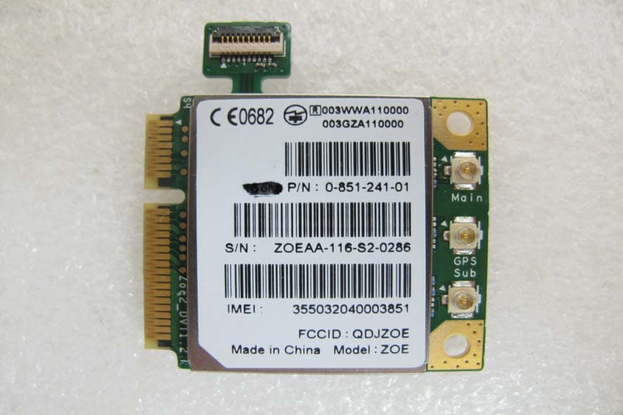
QDJZOE
Feb 21, 20113G Data Module
Equipment Class
PCB - PCS Licensed Transmitter
QDJ-F902
Feb 25, 2010SMART PHONE
Equipment Class
DSS - Part 15 Spread Spectrum Transmitter
QDJ-0602DBS01
Jun 13, 2006Smart Phone
Equipment Class
DTS - Digital Transmission System