QRE21190122 Ch FRS/GMRS Trasceiver - Transmitter Portion
Headline Information & Communication Ltd.
Click to zoom
Application Details
- Equipment Class
- FRF - Part 95 Family Radio Face Held Transmitter
- Date of Grant
- Feb 02, 2003
- Application Purpose
- Original Equipment
- Date of Application
- Dec 11, 2002
- Equipment Note
- 22 Ch FRS/GMRS Trasceiver - Transmitter Portion
- Frequency Range
- 462.56250000 - 467.71250000
- Country
- South Korea
Documents & Files
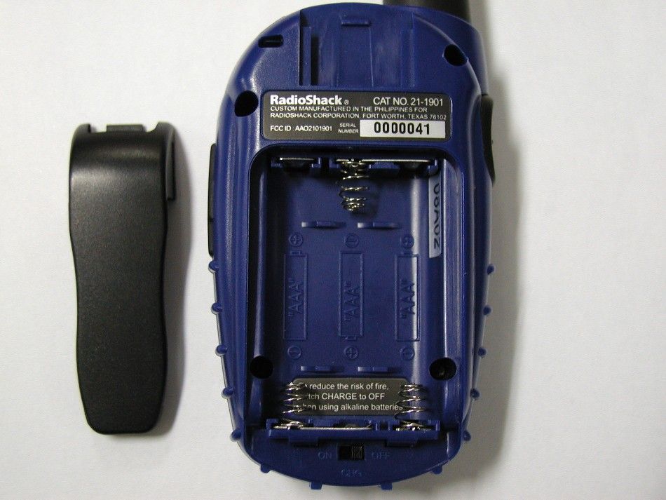
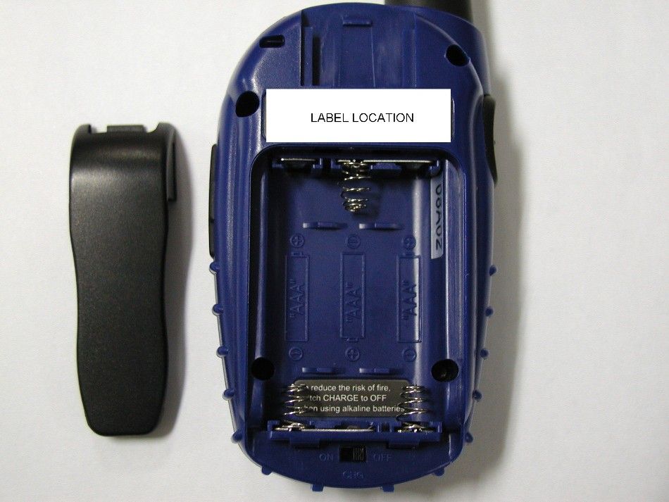
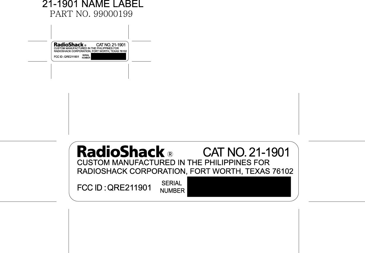

Document Text
Text extracted from the exhibit documents filed with the FCC. Open a document above to read the original.
Operational Description
7.THEORY OF OPERATION Circuit Composition And Operation Theory The basic explanation for the circuit composition 21-1901 consists mainly of the one board controlling the analog circuit parts and the digital circuit parts for the other control. Receiver 21-1901 transmission parts is composed in the double conversion system, which has the 1st IF Frequency of 10.7MHz and the 2nd IF frequency of 450KHz. With the frontend circuit which has an excellent band characteristic and spite characteristic, the Ceramic filter used in the 1st IF, and the 3 pole ceramic filter in the 2nd IF, the reception interrupting factors such as the image and the sensitivity repression are reduced for the more stable reception. RF Frontend The signal received by the antenna will be transmitted to the frontend through the antenna switching circuit consisted of LT6, LT7, CT24, CT23 and CT25. The fronted consists of the RF amplifier transistor QR1, primarily diminishes the other signal rather then the 1st IF image and other signal within the reception band and amplifies only the necessary signal within the RF. 1st Mixer The receiver signal which has been amplified in the RF fronted is provided to the base of the 1st mixer QR2. The 1st L/O signal provide from the PLL circuit is supplied to the emitter of QR2 and converted to the 1st IF 10.7MHz. 1st IF Filter and 1st IF Amplifier The signal covered by QR2 to 10.7MHz, the 1st frequency, change its impedance through LR4 and then is infused to the fundamental CF which has the center frequency of 10.7MHz and the band width of +/- 280KHz. Here, the signal reduces the image and other unwanted signal for the 2`nd IF, Then the signal is infused to the QR3, the 1st IF amplifier. The signal infused to the 41th of the is amplified approximately by 20dB in other to acquire the required reception sensitivity, and infused to the IC8which functions as the 2`nd mixer, the 2`nd IF amplifier, and the FM detector. 2nd Mixer, 2nd IF, FM Detector ( IC8 ) The receiver IF signal of 10.7MHz, which has been infused to IC8 is mixed with the 2nd L/O signal of 10.250MHz, and converted to 450KHz, the 2`nd IF frequency. The receiver signal converted to the 2nd IF frequency passed through the FC2, the ceramic filter of 450KHz again. After the limiting inside the IC8 and the FM demodulating by the quadrature detector inside the IC8, the signal offers the output through the 26th pin of the IC8. The squelch circuit is composed to detect the noises from the received signal demodulate in the 26th pin of the IC8. For this purpose, the noise filter is using the OP amplifier inside the IC8. De-Emphasis The audio signal which has been FM demodulate in the IC8 is supplies to CR16,21,34,35,RR15,17,18 which function as the De-emphasis. Audio Power Amplifier ( IC2) The received audio signal which has been adjusted to the 2nd pin of the IC2 and amplified approximately by 20dB. Then, it turns up the speaker with the maximum output of 0.3Watts. The 3th pin of the IC2 is the audio mute terminal. If a voltage supply to the 7th pin of the IC2 is supplied to this terminal, the IC2 stops functioning as the audio power amplifier regardless of the signal supplied to the 2nd pin of the IC2, and there is no sound from the speaker. Transmitter The transmission part of the 21-1901 is designed to amplify the RF signal oscillated and modulated by the synthesizer to approximately below 0.3(0.23) W by the power transistor of QT3. Pre- emphasis (IC8) The voice signal input from the microphone is pre- emphasized at the 9 th of the IC8. The signal which comes out of the 18 th of the IC8 is limited to a certain amplitude for the voice signal not to exceed the allowable band width assigned for transmission. TX Power ( QT3 ) The transmitted signal of approximately 7mW, combined at the PLL module is supplied to the base of the QT3 amplifier. The transmitted signal amplified to 0.7(0.55) Watts here passes the TX LPF of the 2nd characteristic of the LT4 and the LT5, and RX/TX switching takes place by the DT2. After this, the signal is provided to the antenna the TX LPF of the 1st characteristics, consisted of the LT6. Frequency Synthesizer Voltage Control Oscillator ( VCO ) The VCO of the 21-1901 oscillates 462 ~ 467MHz under the transmission condition and 451 ~ 457MHz under the reception condition. The VCO consists of the colpits oscillator of the QV2, and contains the oscillator frequency of approximately 10.7MHz during the transmission / reception conversion. That is since the VCO should oscillate relatively low frequency during reception compared to transmission, the DV2 is directly biased by the QV1. Therefore as a result, the CV6 is added in parallel to the resonance circuit of the VCO to oscillate a low frequency. During transmission, a relatively high frequency should be oscillate compared to reception. Therefore, the DV2 is adversely biased by the QV1, and as a result, the CV6 which is added in parallel to the resonance circuit of the VCO is removed to oscillate the desired transmission frequency. The VCO is controlled by the IC8 PLL IC in order to oscillate the accurate frequency. The VCO is controlled by the IC8 PLL IC in order to oscillate accurate frequency. The output frequency of the VCO is supplied to the IC8 PLL IC immediately. At the IC8, TCXO(10.25MHz) by the TCXO-1 is compared to the output frequency of the VCO. The VCO is controlled through the loop filter consisted of the RL4, and the CL5 in order to oscillate the stable frequency wanted for the radio. The VCO controlled voltage which voltage passed the loop filter is supplies to the DV1 varactor diode, and the VCO an oscillate the PLL programmed frequency by the capacity varation in the DV1. In addition, the LV2 on the VCO circuit functions as frequency for the VCO to be properly controlled by the IC8 PLL IC. RX/TX Buffer Amplifier ( QF1, QT1 ) The RF signal oscillate at the VCO is provide to the QR2 RX 1st mixer through the QR2 during the reception, and is provide to…
Text truncated - open the document above for the full version.
Parts List/Tune Up Info
9. SEMICONDUCTORS AND FUNCTIONS ) QS1 KRA105S K.E.C RX B+ SWITCHING QS2 KRA105S K.E.C POWER SAVEING SWITCHING QS3 KRA110S K.E.C BACK LIGHT LED CONTROL QS4 KRA105S K.E.C TX B+ SWITCHING QS5 KRA104S K.E.C CPU VDD CINTROL QS6 KRC104S K.E.C TX B+ SWITCHING QS7 KTA1504 K.E.C AUDIO PATH QS8 KRA105S K.E.C VOX DETECTOR QS9 KTC3875S K.E.C VOX DETECTOR QS10 KTA1504 K.E.C PTT INPUT DETECTOR QB1 KTC3875S K.E.C LOW BATT. DET. QB3 KRA105S K.E.C TX POWER CONTROL QF1 2SC4226 N.E.C RX LOCAL OUTPUT QF2 KRC110S K.E.C TX SWITCHING QR1 2SC4226 N.E.C RX RF AMP. QR2 2SC4226 N.E.C 1'ST MIXER QR5 KRC104S K.E.C AUDIO AMP. B+ CONTROL QR6 KRA226S K.E.C AUDIO AMP. B+ CONTROL QT1 2SC4226 N.E.C TX BUFFER QT2 2SC4226 N.E.C TX POWER DRIVE AMP. QT3 DRF1401 PARTSNIC TX POWER FINAL AMP. QV1 KRC104S K.E.C RX/TX MOD. SWITCHING QV2 2SC4226 N.E.C O.S.C ) IC2 NJM2070 J.R.C AUDIO POWER AMP. IC3 TMP87C807U TOSHIBA CPU IC5 TAR5S28 TOSHIBA REGULATOR IC8 AN6311FA MATSUSHITA 2’nd MIXER, IF AMP. AND FM DETECTOR PLL FREQUENCY SYNTHESIZER, MIC PRE AMP., SPK PRE AMP.,
Parts List/Tune Up Info
8.Aligment instructions WARNING Any repairs or adjustments should be made under the supervision of a qualified radio-telephone technician. TRANSMITTER 1. Power Supply Voltage The Power supply voltage should be set for 4.5 VDC measured at the radio during transmit. Periodically check the power supply voltage during the alignment procedure. 2. Frequency Setting A. Connect a frequency counter or Communications Service Monitor to the antenna connector through and RF power attenuator (10 watt minimum rating, 20 dB minimum attenuation). B. Depress the PTT switch. C. Adjust the CTX1 trimmer capacitor such that the output frequency is equal to the channel frequency with a maximum error of +/- 300 Hz. D. Release the PTT switch. 3. Output Power Alignment. A. Set the power supply voltage for 4.5 VDC. B. Connect a Communications Service Monitor or a wattmeter and dummy load to the antenna connector. C. Depress the PTT switch. D. To be convinced for 0.23 Watt output power with a maximum error of +/- 0.05Watt. E. Release the PTT switch. 4. Deviation Adjustment. A. Connect an audio generator to the microphone jack JIG. The audio frequency should be set at 1 KHz. B. Connect an FM deviation meter or Communications Service Monitor to the antenna connector through an RF power attenuator (10 watt minimum rating, 20 dB minimum attenuation). Set the monitor to read peak deviation. C. Depress the PTT switch. D. Adjust the audio generator level 100 mV rms. E. Adjust SV3 for +/- 2.2 KHz maximum deviation. G. Release the PTT switch. RECEIVER NOTE: Insure that the proper channel has been selected before preceding with the alignment procedure. 1. Power Supply Voltage The proper voltage for testing is 4.5 VDC. 2. Receiver Alignment A. Connect an RF signal generator or Communications Service Monitor to the antenna connector. B. Connect a SINAD meter and oscilloscope across the speaker terminals. C. Set the output level of the RF signal generator for - 47 dBm. the generator should be set for +/- 1.5 KHz deviation of a 1 KHz tone. D. Set the audio output level for 0.6 Vrms. by adjusting volume. E. Reduce the output level of the RF signal generator for produce a 8-12 dB SINAD indication. and then confirm more then -118dBm output level of RF signal generator
Test Report
APPLICANT: HEADLINE INFORMATION & COMMUNICATIONS LTD. FCC ID: QRE211901 REPORT #: R\Radsh_AAO\994AUT2\994AUT2TestReport.doc TABLE OF CONTENTS TABLE OF CONTENTS LIST APPLICANT: HEADLINE INFORMATION & COMMUNICATIONS LTD. FCC ID: QRE211901 TEST REPORT: PAGE 1......COVER SHEET - GENERAL INFORMATION & TECHNICAL DESCR. PAGE 2......TECHNICAL DESCRIPTION CONTINUED PAGE 3......RF POWER OUTPUT PAGE 4......MODULATION CHARACTERISTICS PAGE 5......AUDIO FREQUENCY RESPONSE GRAPH PAGE 6......MODULATION LIMITING GRAPH – 300Hz PAGE 7......MODULATION LIMITING GRAPH – 1000Hz PAGE 8......MODULATION LIMITING GRAPH – 2500Hz PAGE 9......AUDIO LOW PASS FILTER GRAPH PAGE 10.....OCCUPIED BANDWIDTH PAGE 11.....OCCUPIED BANDWIDTH PLOT PAGE 12.....OCCUPIED BANDWIDTH PLOT - CW PAGE 13.....SPURIOUS EMISSIONS AT ANTENNA TERMINALS PAGE 14.....UNWANTED RADIATION PAGE 15.....METHOD OF MEASURING RADIATED SPURIOUS EMISSIONS PAGE 16.....FREQUENCY STABILITY PAGE 17-19..LIST OF TEST EQUIPMENT EXHIBITS CONTAINING: EXHIBIT 1.........FCC ID LABEL SAMPLE EXHIBIT 2.........LABEL LOCATION EXHIBIT 3.........EXTERNAL PHOTOGRAPHS EXHIBIT 4.........INTERNAL PHOTOGRAPHS EXHIBIT 5.........BLOCK DIAGRAM EXHIBIT 6.........SCHEMATICS EXHIBIT 7.........USER'S MANUAL EXHIBIT 8.........CIRCUIT DESCRIPTION EXHIBIT 9.........TUNING PROCEDURE EXHIBIT 10........PARTS LIST EXHIBIT 11........TEST SET UP PHOTO APPLICANT: HEADLINE INFORMATION & COMMUNICATIONS LTD. FCC ID: QRE211901 REPORT #: R\Radsh_AAO\994AUT2\994AUT2TestReport.doc Page 1 of 19 GENERAL INFORMATION REQUIRED FOR CERTIFICATION 2.1033(c)(1)(2) HEADLINE INFORMATION & COMMUNICATIONS LTD. will manufacture the FCCID: QRE211901 GMRS/FRS COMB- INATION TRANSCEIVER in quantity, for use under FCC RULES PART 95. HEADLINE INFORMATION & COMMUNICATIONS LTD. 100 THROCKMORTON ST. SUITE 1300 FT. WORTH, TX 76102-2802 2.1033 (c) TECHNICAL DESCRIPTION 2.1033(c)(3) Instruction book. A draft copy of the instruction manual is included as EXHIBIT 7. 2.1033(c) (4) Type of Emission: 9K8F3E 95.631 Bn = 2M + 2DK M = 2500 D = 2.4k Bn = 2(2500)+2(2400) = 9800 GMRS Authorized Bandwidth 20.0 kHz 2.1033(c)(5) GMRS Frequency Range: 1. 462.5500 13. 462.7000 95.621 2. 462.5625 14. 462.7125 3. 462.5750 15. 462.7250 4. 462.5875 16. 467.5500 5. 462.6000 17. 467.5750 6. 462.6125 18. 467.6000 7. 462.6250 19. 467.6250 8. 462.6375 20. 467.6500 9. 462.6500 21. 467.6750 10. 462.6625 22. 467.7000 11. 462.6750 23. 467.7250 12. 462.6875 2.10311c)(6)(7) The Maximum Output Power Rating: GMRS - .23 Watts ERP FRS - .13 Watts ERP FRS Authorized Bandwidth 12.5KHz 2.1033(c)(5) FRS Frequency Range: 1. 462.5625 8. 467.5625 95.627 2. 462.5875 9. 467.5875 3. 462.6125 10. 467.6125 4. 462.6375 11. 467.6375 5. 462.6625 12. 467.6625 6. 462.6875 13. 467.6875 7. 462.7125 14. 467.7125 MHz APPLICANT: HEADLINE INFORMATION & COMMUNICATIONS LTD. FCC ID: QRE211901 REPORT #: R\Radsh_AAO\994AUT2\994AUT2TestReport.doc Page 2 of 19 2.1033(c)(6)(7) Power Output shall not exceed 0.50 Watts effective 95.639 radiated power. There can be no provisions for 95.649 increasing the power or varying the power. 2.1033(c)(8) DC Voltages and Current into Final Amplifier: FINAL AMPLIFIER ONLY FOR LOW POWER SETTING INPUT POWER: (4.5V)(.274A) = 1.233 Watts FOR HIGH POWER SETTING INPUT POWER: (4.5V)(.326A) = 1.467 Watts 2.1033(c)(9) Tune-up procedure. The tune-up procedure is included as EXHIBIT # 9. 2.1033(c)(10) Complete Circuit Diagrams: The circuit diagram is included as EXHIBIT 6 of this report. The block diagrams are included as EXHIBIT 5 of this report. 2.1033(c)(11) A photograph or a drawing of the equipment identification label is included as exhibit No. 1. 2.1033(c)(12) Photographs(8"X10") of the equipment of sufficient clarity to reveal equipment construction and layout, including meters, labels for controls, including any view under shields. See exhibits 3-4. 2.1033(c)(13) Digital modulation is not allowed. 2.1033(c)(14) The data required by 2.1046 through 2.1057 is submitted below. APPLICANT: HEADLINE INFORMATION & COMMUNICATIONS LTD. FCC ID: QRE211901 REPORT #: R\Radsh_AAO\994AUT2\994AUT2TestReport.doc Page 3 of 19 95.639 Power Output shall not exceed 50.0 Watts effective radiated power. There can be no provisions for 95.649 increasing the power or varying the power. 2.1046(a) RF power is measured by the substitution method as outlined in TIA/EIA - 603. With a nominal battery voltage of 4.5 V, and the transmitter properly adjusted the RF output measures: OUTPUT POWER: HIGH: .23 Watts ERP LOW: .13 Watts ERP 2.1046(a) RF power output. The test procedure used was TIA/EIA-603 S2 APPLICANT: HEADLINE INFORMATION & COMMUNICATIONS LTD. FCC ID: QRE211901 REPORT #: R\Radsh_AAO\994AUT2\994AUT2TestReport.doc Page 4 of 19 2.1047(a)(b) Modulation characteristics: AUDIO FREQUENCY RESPONSE The audio frequency response was measured in ac- cordance with TIA/EIA Specification 603. The audio frequency response curve is shown on the next page. The audio signal was fed into a dummy microphone circuit and into the microphone connector. The input required to produce 30 percent modulation level was measured. See Page 5 of report. 2.1047(b) Audio input versus modulation The audio input level needed for a particular per- percentage of modulation was measured in accor- dance with TIA/EIA Specification 603. The audio input curves versus modulation are on the following pages. Curves are provided for audio input frequen- cies of 300, 1000, and 2500 Hz. See Pages 6,7 & 8 of report. 95.637 Post Limiter Filter Each GMRS transmitter, except a mobile station transmitter with a power of 2.5Watts or less, must be equipped with an audio low pass filter. At any frequency between 3 & 20 kHz the filter must have an attenuation of 60log (f/3) greater than the attenuation at 1 kHz. See Page 9 of report. APPLICANT: HEADLINE INFORMATION & COMMUNICATIONS LTD. FCC ID: QRE211901 REPORT #: R\Radsh_AAO\994AUT2\994AUT2TestReport.doc Page 5 of 19 AUDIO FREQUENCY RESPONSE GRAPH Radio Shack Corp. 21-1901 -56 -51 -46 -41…
Text truncated - open the document above for the full version.
Contact Information
Applicant
Jaeseok Lee(General Manager)
Technical Contact
Timco Engineering, Inc.Mario R de Aranzeta
[email protected]888-472-2424
849 NW State Road 45 · Newberry, Florida · United States
Non-Technical Contact
Timco Engineering, Inc.Sharon A Hoffman
[email protected]888-472-2424
Test Firm
Timco Engineering, Inc.S Sanders
Technical Specifications
| # | Rule Parts | Frequency Range | Power Output | Emission | Tolerance |
|---|---|---|---|---|---|
| 2 | 95B | 462.5625 MHz - 467.7125 MHz | 130.00 mW | 9K80F3E | 2.5 ppm |
Other Applications from Headline Information & Communication Ltd.

QREHL-10V2
Dec 30, 2004VHF TRANSCEIVER-TRANSMITTER
Equipment Class
TNF - Licensed Non-Broadcast Transmitter Held to Face
QREHL-10U1
Dec 30, 2004UHF Transceiver
Equipment Class
TNF - Licensed Non-Broadcast Transmitter Held to Face
QREHL-10U2
Dec 30, 2004UHF Transceiver
Equipment Class
TNF - Licensed Non-Broadcast Transmitter Held to Face
QREHL-10V2L
Dec 29, 2004VHF TRANSCEIVER
Equipment Class
TNB - Licensed Non-Broadcast Station Transmitter