QTG-ZKMSBluetooth Module
ZAGG Inc.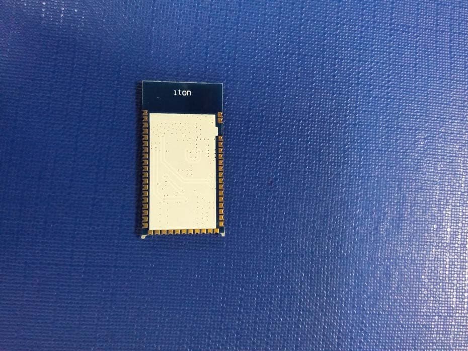
Click to zoom
Application Details
- Equipment Class
- DSS - Part 15 Spread Spectrum Transmitter
- Date of Grant
- Nov 20, 2014
- Application Purpose
- Original Equipment
- Date of Application
- Nov 20, 2014
- Equipment Note
- Bluetooth Module
- Frequency Range
- 2402.00000000 - 2480.00000000
- Company
- ZAGG Inc.
- Country
- United States
Documents & Files
Document Text
Text extracted from the exhibit documents filed with the FCC. Open a document above to read the original.
Users Manual
ITON TECHNOLOGY LTD. Bluetooth 3.0 HID Module 1 Office Add.: Room 1302, Block A, Building 4, Tianan Cyber Park, Huangge Road, Longgang District, Shenzhen, Guangdong, China Tel: 86-755-82079392,82078660Fax: 86-755-82079390July 28,2011 Product: Module Number: FCC ID: Bluetooth 3.0 HID Module ,Class 2 BT3GMD-B47P User Manual ID6ZFN-BK0 Brand name: ZAGG QTG-ZKMS ITON TECHNOLOGY LTD. Bluetooth 3.0 HID Module Section 1:Overview The BT3GMD-B47P is a Bluetooth Human Interface Device(HID) module based on the Broadcom BCM20730 Bluetooth 3.0 specification basic rate-compliant stand alone baseband processor with an integrated 2.4GHz transceiver. The module includes EEPROM, crystal, and PCB antenna. 1.1 Applications ● Wireless pointing devices: mice ,trackballs , gestural controls ● Wireless keyboards ● 3D glasses ● Game controllers ● Point-of-sale(POS)input devices ● Remote sensors ●Home automation ● Personal health and fitness monitoring 1.2 Features The BT3GMD-B47P offers the following features: ● On-chip support for common keyboard and mouse interfaces eliminates external processor ● Programmable keyscan matrix interface, up to 8×20 key-scanning matrix ● Bluetooth specification 3.0 compatible, includeing enhanced power control ● Bluetooth HID profile version 1.0 compliant ● Bluetooth Device ID profile version 1.3 compliant ● Bluetooth AVRCP-CT profile version 1.3 compliant ● Supports Adaptive Frequency Hopping(AFH) ● On-chip support for serial peripheral interface(SPI) ● Programmable output power control meets Class 2 or Class 3 requirements ● Excellent receiver sensitivity ● Integrated ARM Cortex TM -M3 based ● On-chip power-on reset(POR) 1.3 Functional Description The primary component on the module is the Broadcom BCM20730, which is a Bluetooth 3.0 compliant basic rate single-chip. The baseband and radio have been integrated into a single chip implementedin standard digital CMOS. The block diagram of the module is shown in Figure 1. ITON TECHNOLOGY LTD. Bluetooth 3.0 HID Module Figure 1: Block Diagram The BT3GMD-B47P employs an integrated ARM Cortex TM -M3 microprocessor core that runs software from the Link Control layerup to the Host Controller Interface (HCI).The baseband portion of the BT3GMD-B47P performs all the time-critical functions required for high-performance Bluetooth operations. The radio incorporates the complete receive and transmit paths, including PLL, VCO, LNA, PA, upconverter,downconverter, modulator, demodulator, and channel select filtering. The BT3GMD-B47P on-chip keyboard scanner is designed to autonomously sample keys and store them into buffer registers without requiring host microcontroller intervention. A state machine of three states(Idle, Scan, and Scan-End)controls the keyscan block. The module has a SPI interface. The interface has a 16-byte transmit buffer and a 16-byte receive buffer .To support more flexibility for user applications. The module acts as an SPI master device that supports 1.8V or 3.3V SPI slaves. ITON TECHNOLOGY LTD. Bluetooth 3.0 HID Module 1.4 Physical Description The BT3GMD-B47P is a 28.5mm×15mm FR4 PCB with 47 pads located around the perimeter. Table 1 shows the pinout diagram of the module. Table 1 Pin Location Figure 2: Module PCB Top View PINSignalPIN SignalPIN SignalPIN SignalPIN Signal 1GND2GND3P134P85P17 6P227UP_TX8UP_RX9P610P0 11P112P513P414P215P31 16RESET17P318SDA19SCL20P32 21P1622P1823P1924P2525VDD 26GND27P2028P2429P2130P7 31P2932P2833P2734P2635P36 36P3037P3838P3739P1540P14 41P1242 P9 43P2344P1145P10 46GND47GND 28.5mm 15mm ITON TECHNOLOGY LTD. Bluetooth 3.0 HID Module Table 2 Pin Function Descriptions Pi n Number Pi n Name Default Direction POR State Function Description 1 , 2 , 26 , 46 , 47 GNDGround 25VDDPower supply 16RESETPUActive-low system reset with open-drain output & internal pull up resistor 18SDAI/OPU Data signal for an extern I 2 C device 19SCLI/OPU Clock signal for an extern I 2 C device 7UP_TXoutputPUUART serial output-serial data output for the HCI UART interface 8UP_RXinputUART serial input-serial data output for the HCI UART interface 10P0inputFloating GPIO:P0,Keyboard scan input(row):KSI0 11P1inputFloating GPIO:P1,Keyboard scan input(row):KSI1 14P2inputFloating GPIO:P2,Keyboard scan input(row):KSI2 17P3inputFloating GPIO:P3,Keyboard scan input(row):KSI3 13P4inputFloating GPIO:P4,Keyboard scan input(row):KSI4 12P5inputFloating GPIO:P5,Keyboard scan input(row):KSI5 9P6inputFloating GPIO:P6,Keyboard scan input(row):KSI6 30P7inputFloating GPIO:P7,Keyboard scan input(row):KSI7 4P8inputFloating GPIO:P8,Keyboard scan output(column):KSO0 42P9inputFloating GPIO:P9,Keyboard scan output(column):KSO1 45P10inputFloating GPIO:P10,Keyboard scan output(column):KSO2 44P11inputFloating GPIO:P11,Keyboard scan output(column):KSO3 41P12inputFloating GPIO:P12,Keyboard scan output(column):KSO4 3P13inputFloating GPIO:P13,Keyboard scan output(column):KSO5 40P14inputFloating GPIO:P14,Keyboard scan output(column):KSO6 39P15inputFloating GPIO:P15,Keyboard scan output(column):KSO7 21P16inputFloating GPIO:P16,Keyboard scan output(column):KSO8 5P17inputFloating GPIO:P17,Keyboard scan output(column):KSO9 22P18inputFloating GPIO:P18,Keyboard scan output(column):KSO10 23P19inputFloating GPIO:P19,Keyboard scan output(column):KSO11 27P20inputFloating GPIO:P20,Keyboard scan output(column):KSO12 29P21inputFloating GPIO:P21,Keyboard scan output(column):KSO13 6P22inputFloating GPIO:P22,Keyboard scan output(column):KSO14 43P23inputFloating GPIO:P23,Keyboard scan output(column):KSO15 28P24inputFloating GPIO:P24,Keyboard scan output(column):KSO16 24P25inputFloating GPIO:P25,Keyboard scan output(column):KSO17,SPI MISO (Master mode) 34P26inputFloating GPIO:P26,Current 16 mA @3.3V 33P27inputFloating GPIO:P27,Current 16 mA @3.3V 32P28inputFloating GPIO:P28,Current 16 mA @3.3V 31P29inputFloating GPIO:P29,Current 16 mA @3.3V 36P30inputFloating GPIO:P30,A/D converter input,Default as the battery capacity detection 15P31inputFloating GPIO:P31, A/D converter input,…
Text truncated - open the document above for the full version.
Cover Letter(s)
Nov.14, 2014 Federal Communication Commission Authorization and Evaluation Division FCC ID: QTG-ZKMS Re: Confidentiality Request Pursuant to Sections 0.457 and 0.459 of the Commission’s Rules, the applicant hereby requests confidential treatment of information applied this application as outlined below: 1: Block Diagram 2: Circuit Diagram 3: Parts List 4.Operational Description The above materials contain trade secrets and proprietary information not customarily released to the public. The public disclosure of these matters might be harmful to the applicant and provide unjustified benefits to its competitors. The Applicant understands that pursuant to Rules 0.457, disclosure of this Application and all accompanying documentation will not be made before the date of the Grant for this application. Sincerely, ZAGG Inc. Contact person: Paul Faerber Title: Director of Product Development
Cover Letter(s)
Applicant ZAGG Inc. FCC ID: QTG-ZKMS Section 15.212 Modular Transmitters Request for Modular Approval N/A Request for Limited Modular Approval Y Requirements EUT Conditions Comply (Y/N) Single Modular Approval Requirements 1 The radio elements of the modular transmitter must have their own shielding. The physical crystal and tuning capacitors may be located external to the shielded radio elements. No, this RF Module has no own RF shielding and therefore does not comply to this requirement. Limited Modular Approval is applied. The RF Module is subject to Professional Installation and Integrator is advised by the integration manual how to assure compliance of final end-product into which this RF Module is integrated to the FCC regulations. N 2 The modular transmitter must have buffered modulation/data inputs (if such inputs are provided) to ensure that the module will comply with Part 15 requirements under conditions of excessive data rates or over-modulation. Please refer the Schematic, The modular transmitter have buffered modulation/data inputs U1 Y 3 The modular transmitter must have its own power supply regulation. Complies, this RF Module has own power supply regulation, please refer to schematics (U1). Y 4 The modular transmitter must comply with the antenna and transmission system requirements of Sections 15.203, 15.204(b) and 15.204(c). The antenna must either be permanently attached or employ a “unique” antenna coupler (at all connections between the module and the antenna, including the cable). The “professional installation” provision of Section 15.203 is not applicable to modules but can apply to limited modular approvals under paragraph (b) of this section. Referring to onboard PCB antenna Y 5 The modular transmitter must be tested in a stand-alone configuration, i.e., the module must not be inside another device during testing for compliance with Part 15 requirements. Unless the transmitter module will be battery powered, it must comply with the AC line conducted requirements found in Section 15.207. AC or DC power lines and data input/output lines connected to the module must not contain ferrites, unless they will be marketed with the module (see Section 15.27(a)). The length of these lines shall be the length typical of actual use or, if that length is unknown, at least 10 centimeters to insure that there is no coupling between the case of the module and supporting equipment. Any accessories, peripherals, or support equipment connected to the module during testing shall be unmodified and commercially available equipment. Any accessories, peripherals, or support equipment connected to the module during testing shall be unmodified and commercially available (see Section 15.31(i)). Does not comply. Due to the fact that this RF Module is not equipped with an own RF shielding, the radiated measurements are performed with the RF Module installed in a dedicated host / host platform (here BT Keyboard). N 6 The modular transmitter must be equipped with either a permanently affixed label or must be capable of electronically displaying its FCC identification number. (A) If using a permanently affixed label, the modular transmitter must be labeled with its own FCC identification number, and, if the FCC identification number is not visible when the module is installed inside another device, then the outside of the device into which the module is installed must also display a label referring to the enclosed module. This exterior label can use wording such as the following: “Contains Transmitter Module FCC ID: QTG-ZKMS” or “Contains FCC ID: QTG-ZKMS.” Any similar wording that expresses the same meaning may be used. The Grantee may either provide such a label, an example of which must The modular was labeled with its own FCC ID. The outside of device in to which the module is installed will labeled ‘Contains TX FCC ID:QTG-ZKMS, Please refer to User Manual Y be included in the application for equipment authorization, or, must provide adequate instructions along with the module which explain this requirement. In the latter case, a copy of these instructions must be included in the application for equipment authorization. (B) If the modular transmitter uses an electronic display of the FCC identification number, the information must be readily accessible and visible on the modular transmitter or on the device in which it is installed. If the module is installed inside another device, then the outside of the device into which the module is installed must display a label referring to the enclosed module. This exterior label can use wording such as the following: “Contains FCC certified transmitter module(s).” Any similar wording that expresses the same meaning may be used. The user manual must include instructions on how to access the electronic display. A copy of these instructions must be included in the application for equipment authorization. 7 The modular transmitter must comply with any specific rules or operating requirements that ordinarily apply to a complete transmitter and the manufacturer must provide adequate instructions along with the module to explain any such requirements. A copy of these instructions must be included in the application for equipment authorization. This RF Module will exclusively integrated into battery power host devices. The integration limitations are clearly addressed within the integration manual, please refer to the User Manual. Y 8 The modular transmitter must comply with any applicable RF exposure requirements in its final configuration. With the documented max output power this RF Module meets the FCC SAR Exemption,so it can comply with any applicable RF exposure requirements in its final configuration. Y A limited modular approval may be granted for single or split modular transmitters that do not comply with all of the above requirements, e.g., shielding, minimum signaling amplitude, buffered modulation/data inputs, or power supply regulation, if th…
Text truncated - open the document above for the full version.
External Photos
External Photos APPENDIX B: PHOTOGRAPHS OF EUT
ID Label/Location Info
FCC ID Label Location FCC ID:QTG‐ZKMS
Internal Photos
Internal Photos
Test Report
Page 1 of 51 FCC Test Report Report No.: AGC00918141005FE03 FCC ID : QTG‐ZKMS APPLICATION PURPOSE : Original Equipment PRODUCT DESIGNATION : BT3GMD‐B47P BRAND NAME : ZAGG MODEL NAME : See page 5 CLIENT : ZAGG Inc. DATE OF ISSUE : Nov.13,2014 STANDARD(S) : FCC Part 15 Rules REPORT VERSION : V1.0 Attestation of Global Compliance (Shenzhen) Co., Ltd CAUTION: This report shall not be reproduced except in full without the written permission of the test laboratory and shall not be quoted out of context. Report No.: AGC00918141005FE03 Page 2 of 51 Report Revise Record Report Version Revise Time Issued Date Valid VersionNotes V1.0 / Nov.13,2014 Valid Original Report Report No.: AGC00918141005FE03 Page 3 of 51 TABLE OF CONTENTS 1. VERIFICATION OF CONFORMITY ...................................................................................... 5 2. GENERAL INFORMATION .................................................................................................. 6 2.1. PRODUCT DESCRIPTION ........................................................................................................... 6 2.2. TABLE OF CARRIER FREQUENCYS .......................................................................................... 6 2.3. RECEIVER INPUT BANDWIDTH ................................................................................................. 7 2.4. EXAMPLE OF A HOPPING SEQUENCY IN DATA MODE ........................................................... 7 2.5. EQUALLY AVERAGE USE OF FREQUENCIES AND BEHAVIOUR ............................................ 7 2.6. RELATED SUBMITTAL(S) / GRANT (S) ....................................................................................... 8 2.7. TEST METHODOLOGY................................................................................................................ 8 2.8. SPECIAL ACCESSORIES ............................................................................................................ 8 2.9. EQUIPMENT MODIFICATIONS ................................................................................................... 8 3. MEASUREMENT UNCERTAINTY........................................................................................ 9 4. DESCRIPTION OF TEST MODES ........................................................................................ 9 5. SYSTEM TEST CONFIGURATION .................................................................................... 10 5.1. CONFIGURATION OF EUT SYSTEM ........................................................................................ 10 5.2. EQUIPMENT USED IN EUT SYSTEM ....................................................................................... 10 5.3. SUMMARY OF TEST RESULTS ................................................................................................ 10 6. TEST FACILITY .................................................................................................................. 11 7. PEAK OUTPUT POWER .................................................................................................... 12 7.1. MEASUREMENT PROCEDURE ................................................................................................ 12 7.2. TEST SET-UP (BLOCK DIAGRAM OF CONFIGURATION) ....................................................... 12 7.3. LIMITS AND MEASUREMENT RESULT .................................................................................... 13 8. 20DB BANDWIDTH ............................................................................................................ 15 8.1. MEASUREMENT PROCEDURE ................................................................................................ 15 8.2. TEST SET-UP (BLOCK DIAGRAM OF CONFIGURATION) ....................................................... 15 8.3. LIMITS AND MEASUREMENT RESULTS .................................................................................. 15 9. CONDUCTED SPURIOUS EMISSION ............................................................................... 18 9.1. MEASUREMENT PROCEDURE ................................................................................................ 18 9.2. TEST SET-UP (BLOCK DIAGRAM OF CONFIGURATION) ....................................................... 18 9.3. MEASUREMENT EQUIPMENT USED ....................................................................................... 18 9.4. LIMITS AND MEASUREMENT RESULT .................................................................................... 18 10. RADIATED EMISSION ..................................................................................................... 22 10.1. MEASUREMENT PROCEDURE .............................................................................................. 22 10.2. TEST SETUP ............................................................................................................................ 24 10.3. TEST RESULT .......................................................................................................................... 24 Report No.: AGC00918141005FE03 Page 4 of 51 11. BAND EDGE EMISSION .................................................................................................. 31 11.1. MEASUREMENT PROCEDURE .............................................................................................. 37 11.2. TEST SET-UP ........................................................................................................................... 37 11.3. TEST RESULT .......................................................................................................................... 38 12. NUMBER OF HOPPING FREQUENCY ............................................................................ 42 12.1. MEASUREMENT PROCEDURE .............................................................................................. 42 12.2. TEST SETUP (BLOCK DIAGRAM OF CONFIGURATION) .............................................…
Text truncated - open the document above for the full version.
Test Setup Photos
APPENDIX IV PHOTOGRAPHS OF TEST SETUP FCC RADIATED EMISSION TEST SETUP Host device
Contact Information
Applicant
Dan Oakeson(Director of Product Development)
Test Firm
Attestation of Global Compliance Shenzhen Co. Ltd.Forrest Lei
Technical Specifications
| # | Rule Parts | Frequency Range | Power Output |
|---|---|---|---|
| 1 | 15C | 2.40 GHz - 2.48 GHz | 590.00 µW |
Other Applications from ZAGG Inc.

QTG-ZKPXN
Jul 23, 2026Bluetooth Keyboard
Equipment Class
DTS - Digital Transmission System
QTG-ZWSAPUNI58-2
Sep 10, 2024Pro stylus 2
Equipment Class
DTS - Digital Transmission System
QTG-ZKPIB13
Sep 04, 2024Pro Keys 2
Equipment Class
DTS - Digital Transmission System
QTG-ZWCIHSTK
Jul 21, 2024Magnetic Wireless Charger
Equipment Class
DCD - Part 15 Low Power Transmitter Below 1705 kHz
QTG-ZMIHSTK
Jul 13, 2024Mouse
Equipment Class
DTS - Digital Transmission System