QTWG066FRS/GMRS
China & HongKong Telecom Engineering Company Ltd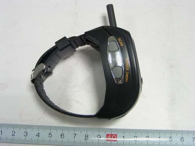
Click to zoom
Application Details
- Equipment Class
- FRF - Part 95 Family Radio Face Held Transmitter
- Date of Grant
- May 03, 2007
- Application Purpose
- Original Equipment
- Date of Application
- May 03, 2007
- Equipment Note
- FRS/GMRS
- Frequency Range
- 467.56250000 - 467.71250000
- Country
- Hong Kong
Documents & Files
Document Text
Text extracted from the exhibit documents filed with the FCC. Open a document above to read the original.
Users Manual
PMR/GMRS G-006
Users Manual
FCC caution: Note: This equipment has been tested and found to comply with the limits for a Class B digital device, pursuant to part 15 of the FCC Rules. These limits are designed to provide reasonable protection against harmful interference in a residential installation. This equipment generates, uses and can radiate radio frequency energy and, if not installed and used in accordance with the instructions, may cause harmful interference to radio communications. However, there is no guarantee that interference will not occur in a particular installation. If this equipment does cause harmful interference to radio or television reception, which can be determined by turning the equipment off and on, the user is encouraged to try to correct the interference by one or more of the following measures: —Reorient or relocate the receiving antenna. —Increase the separation between the equipment and receiver. —Connect the equipment into an outlet on a circuit different from that to which the receiver is connected. —Consult the dealer or an experienced radio/TV technician for help. FCC 15.21 Modifications not authorized by the manufacturer may void users authority to operate this device. FCC 15.19 This device complies with part 15 of the FCC Rules. Operation is subject to the following two conditions: (1) This device may not cause harmful interference, and (2) this device must accept any interference received, including interference that may cause undesired operation.
External Photos
External Photos EUT-Front View EUT-Left Side View EUT-Right Side View
ID Label/Location Info
ID Label/Location FCC ID Label Information Specifications : Text is Black or white in color and is left justified. Labels are printed in indelible ink on permanent adhesive backing or silk-screened onto the EUT or shall be affixed at a conspicuous location on the EUT. FCC ID Label: Proposed Label Location: FCC ID: QTWG066
Internal Photos
Internal Photos EUT-Inside View (1) EUT-Inside View (2) EUT-Inside View (3) EUT-PCB View (1) EUT-PCB View (2) Battery View
Operational Description
Circuit Description I.Transmission section. 1. Audio frequency amplifying section. MIC signal input @pin9 of U8, through amplification and compressor of U8 , The output signal @pin16 goes to FM modulation. 2. VCO section. Q301, Q302 work as VCO, the varactor D302 value i3 controlled by PLL Part of U8 . 3. Power amplifying section. Q11 is a buffer, Q4 is a driver transister,Q1,Q2,Q3 work together as power amplifier. When the signal has been amplified , it will be passed to a switch diode D2 and send out from antenna. II.Receiving section. 1. RF section. The signal received by antenna passed to filter network, then amplified by Q6, via band-pass filter network, then goes into mixer Q8. 2. Local oscillator and Mixer. Q7 is frequency mixing transistor, the VCO act as local oscillator , the frequency is controlled by PLL, after mixing, the IF(21.4MHZ) signal selected by CF1, then output via L12 and C54 to U8. 3. IF section. CF1 is 21.4MHz crystal filter, second IF is 450KHz, U8 works as second mixing, second local-oscillator, second IF amplifier, demodulation etc. 4. Audio section: The demodulated audio signal goes to U4 and is amplified, and then U8 drives Speaker. III.Others. The PLL circuit is embedded in U8, X202 is a local oscillation crystal, CT201 is a trimmer, the U8 pin 46 output constant current to control D302 oscillation frequency.
Test Report
Note: This test report is for the customer shown above and their specific product only. It may not be duplicated or used in part without prior written consent from Bay Area Compliance Laboratory Corp. (Shenzhen). This report must not be used by the customer to claim product certification, approval, or endorsement by NVLAP, NIST, or any agency of the Federal Government 1) FCC PART 95 EMI MEASUREMENT AND TEST REPORT For China and Hong Kong Telecom Engineering Co Ltd Unit 608, 6/F, New Tech Plaza, 34 Tai Yau Street, San Po Kong , Kowloon, Hong Kong. FCC ID: QTWG066 This Report Concerns: Original Report Equipment Type: FRS/GMRS Test Engineer: William Chan Report No.: RSZ07030101 Test Date: 2007-03-09 to 2007-03-14 Report Date: 2007-03-16 Reviewed By: EMC Manager: Boni Baniqued Prepared By: Bay Area Compliance Laboratory Corp. (Shenzhen) 6/F, the 3rd Phase of WanLi Industrial Building, ShiHua Road, FuTian Free Trade Zone Shenzhen, Guangdong, China Tel: +86-755-33320018 Fax: +86-755-33320008 China and Hong Kong Telecom Engineering Co Ltd FCC ID: QTWG066 Report #: RSZ07030101 Page 2 of 23 FCC PART 95 Report TABLE OF CONTENTS GENERAL INFORMATION.......................................................................................................................................3 PRODUCT DESCRIPTION FOR EQUIPMENT UNDER TEST (EUT) .....................................................................................3 OBJECTIVE...................................................................................................................................................................3 RELATED SUBMITTAL(S)/GRANT(S).............................................................................................................................3 TEST METHODOLOGY..................................................................................................................................................3 TEST FACILITY.............................................................................................................................................................3 SYSTEM TEST CONFIGURATION ..........................................................................................................................4 DESCRIPTION OF TEST CONFIGURATION......................................................................................................................4 EQUIPMENT MODIFICATIONS.......................................................................................................................................4 CONFIGURATION OF TEST SETUP.................................................................................................................................5 BLOCK DIAGRAM OF TEST SETUP................................................................................................................................5 SUMMARY OF TEST RESULTS ...............................................................................................................................6 §1.1310 and §2.1093 – RF EXPOSURE .......................................................................................................................7 STANDARD APPLICABLE..............................................................................................................................................7 MEASUREMENT RESULT: .............................................................................................................................................7 §2.1046, §95.135 and §95.639(d) - RF OUTPUT POWER .........................................................................................8 APPLICABLE STANDARD..............................................................................................................................................8 TEST EQUIPMENT LIST AND DETAILS...........................................................................................................................8 TEST PROCEDURE........................................................................................................................................................8 TEST DATA..................................................................................................................................................................9 §2.1047 and §95.637(a) - MODULATION CHARACTERISTIC ...........................................................................10 APPLICABLE STANDARD............................................................................................................................................10 TEST EQUIPMENT LIST AND DETAILS.........................................................................................................................10 TEST PROCEDURE......................................................................................................................................................10 TEST DATA................................................................................................................................................................10 §2.1049 and § 95.633(a) (c) – OCCUPIED BANDWIDTH ......................................................................................14 APPLICABLE STANDARD............................................................................................................................................14 TEST EQUIPMENT LIST AND DETAILS.........................................................................................................................14 TEST PROCEDURE......................................................................................................................................................14 TEST DATA................................................................................................................................................................14 §2.1053 and §95.635(b) (7) - UNWANTED RADIATION EMISSIONS ......................................................…
Text truncated - open the document above for the full version.
Test Setup Photos
Test Setup Photos Radiated Emissions-Front View (Above 1 GHz) Radiated Emissions-Rear View (Above 1GHz) Radiated Emissions-Front View (30-1000 MHz) Radiated Emissions-Rear View (30-1000 MHz)
Contact Information
Applicant
Kam Lun LAI(Sales & Marketing Manager)
Test Firm
Bay Area Compliance Laboratory Corp. (Shenzhen)John Chan
Technical Specifications
| # | Rule Parts | Frequency Range | Power Output | Emission | Tolerance |
|---|---|---|---|---|---|
| 3 | 95B | 467.5625 MHz - 467.7125 MHz | 79.00 mW | 11K0F3E | 2.5 ppm |
Other Applications from China & HongKong Telecom Engineering Company Ltd

QTW-CHKTC
Apr 14, 2003Transmitter Portion of 14 Channel FRS
Equipment Class
FRF - Part 95 Family Radio Face Held Transmitter