RBBMPFP000B0F0PCS Repeater
MPF Technologies, Inc.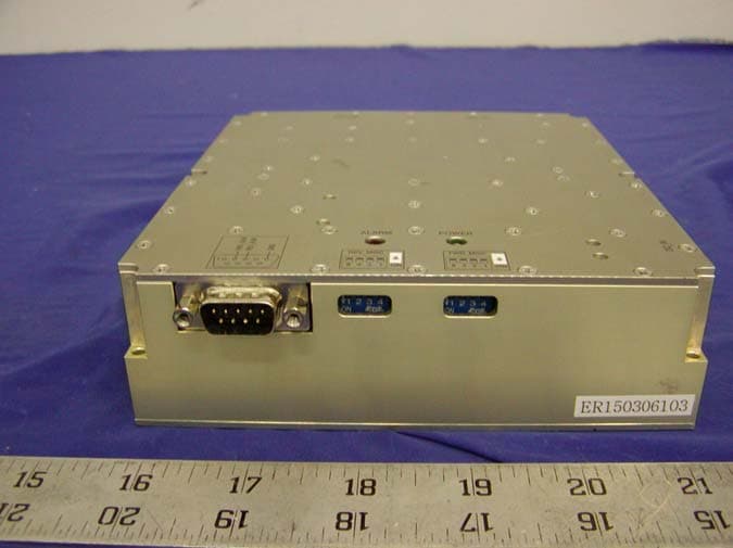
Click to zoom
Application Details
- Equipment Class
- AMP - Amplifier
- Date of Grant
- Sep 22, 2003
- Application Purpose
- Original Equipment
- Date of Application
- Sep 22, 2003
- Equipment Note
- PCS Repeater
- Frequency Range
- 1970.04000000 - 1974.92000000
- Company
- MPF Technologies, Inc.
- Country
- United States
Documents & Files
Document Text
Text extracted from the exhibit documents filed with the FCC. Open a document above to read the original.
Users Manual
1 MPF Technologies MPF-001 Installation and Operations Manual MPF Technologies, Inc. c/o Site Management Services, Inc. 5440 Trabuco Road Irvine, CA 92620 Tel: (949) 387-0194 Fax: (949) 387-6203 E-mail: [email protected] 2 Table of Contents 1. General Information 1.1 Introduction 1.2 Specifications 1.3 Description 2. Installation 2.1 Introduction 2.2 Unpacking and Inspection 2.3 Preparation for Use 2.4 Before Installation 2.5 Antenna Installation 2.6 Repeater Installation 2.7 Connectors 3. Operation 3.1 Introduction 3.2 Operating Instructions 4. Trouble Shooting 5. Drawings 3 1. General Information 1.1 Introduction This manual provides information pertaining to the installation and operation of MPF Technologies’ MPF-001 “Compact Outdoor” repeater. This unit is designed to operate in the 1900 MHz band and the frequency allocation is listed in Table 1-1. This repeater will work for CDMA, TDMA and GSM modulations. <Table 1-1: MPF-001 Repeater> Model Number Down Link* Frequencies Up Link** Frequencies Modulation MPF-001 1950 ~ 1965, 1970 ~ 1975 [MHz] 1870 ~ 1885, 1890~1895 [MHz] CDMA, GSM, TDMA *: Down Link (= Forward Path) is from the BTS (Base Station) to the mobile **: Up Link (= Reverse Path) is from the mobile to the BTS (Base Station) 4 1.2 Specifications Down Link 1950 ~ 1965, 1970 ~ 1975 [MHz] Frequency Range (MHz) Up Link 1870 ~ 1885, 1890~1895 [MHz] Output Power Range (dBm) (max) 15 [dBm] @ 1 channel 10 [dBm] @ 2 channels 7 [dBm] @ 4 channels Input Power Range (dBm) -35 [dBm] Max. Gain (dB) 45~60 / 45~60 [dB] (Adjustable 15dB, 1dB step) Gain Flatness (± dB) ± 2 [dB] (or 4 dB peak to peak) OIP3 (dBm) > +30 [dBm] Shutdown Level ≥ +17 dBm Noise Figure (dB) ≤ 6 [dB] @ Max Gain Group Delay (uS) ≤ 5 [uS] VSWR ≤ 1.5:1 Impedance (ohm) 50 [ohm] Spurious (Freq/dBc) Meets FCC specifications (radiated and conducted). Conducted: ≤ -13 dBm @ 30 MHz ~ 10 GHz, Radiated: ≤ 43 + 10 log (P) dB @ 30 MHz ~ 10 GHz Status LED Power: GREEN, Fail: RED Alarm Port The interface can be an analog +5V circuit that goes off when the system looses power or stops transmitting an RF signal. Alarm Signal Format Normal: 0 V, Abnormal: +5V (TTL) Connector Type & Pin Map 9 Pin D-SUB (M): 2. TX Alarm, 3. RX Alarm, 5.GND, Other Pins. N/C Power Supply External AC/DC Adaptor 6 [V] / 1.2A (Typ), 1.5A (Max) Dimension (W x H x D, inch) 5.55 x 6.34 x 1.65 inch Weight (Pounds) 3.3 lbs RF Connector Type (Input, Output) N-type Female, N-type Female Operating Temperature (°C) -5 to 40 [°C] Cooling Method Convection 5 1.3 Description This repeater is designed for outdoor purposes (e.g. light poles, utility poles etc.) and will improve the PCS communications signal by extending the coverage of a base station. 2. Installation 2.1 Introduction This section provides information for the installation and setup of the MPF-001 repeater. The information consists of procedures for unpacking, inspection and preparation for the actual installation as well as the setup. 2.2 Unpacking and Inspection Examine the shipping carton for damage before unpacking the unit. If the shipping carton is damaged, try to have the carrier’s agent present when the equipment is unpacked. If visual inspection reveals physical damage(s) to the equipment, you should send it back for replacement. 2.3 Preparation for Use 2.3.1 Power Requirements The power supply of the MPF-001 accepts 6 VDC / 1.2 Amperes. Power consumption of the MPF-001 repeater is approximately 7.2 Watts. 2.3.2 Operating Environment The MPF-001 is intended for outdoor use only. For normal conditions, the environmental conditions should be as follows: Temperature range: -5 °C ~ 40 °C 2.4 Before Installation You will need to determine the following before beginning the MPF-001 installation: a. Base station location b. Location where the donor antenna is to be installed c. Location where the server antenna is to installed d. Location where the MPF-001 repeater is to be installed e. Length and type of coaxial cable needed to connect from the donor antenna to the repeater unit 6 f. Length and type of cable needed to connect from the repeater unit to the server antenna 2.5 Antenna Installation 2.5.1 Donor Antenna Select a site where the signal strength from the base station is sufficient enough. Using a coax cable, connect the antenna to the repeater. If you are using a directional antenna such as a Yagi type, the antenna should be installed so that it is in the line of sight of the base station. Then, align the directional antenna toward that direction, and secure the antenna using provided mounting hardware. 2.5.2 Server Antenna Using a coax cable, connect the antenna to the repeater. For this type of antenna, it is usually recommended to use a Patch type since it requires a wider beam width and less directivity. 2.6 Repeater Installation MPF-001 is an outdoor repeater. This repeater can’t be mounted outdoors by itself unless it is installed within an enclosure that meets all the environmental conditions. 2.6.1 Turn-On Procedure Verify all RF connectors are tightened and cables and antennas are secured. Connect AC/DC adaptor on the repeater’s DC Power IN connector. The Power indicator LED should turn Green once plugged in. 2.6.2 Antenna Isolation and Alignment MPF-001 is equipped with an over drive protection circuit. If the output power level of reverse path (Up Link) exceeds prescribed limit, then reverse path is disconnected and the ALARM LED (RED) is on. A. Antenna Alignment The donor and the server antennas needs to be mounted at least some specified distance away from each other, depending on the gains of the antennas. Otherwise, the repeater could go on oscillation and the repeater will shut down automatically and turn back on after a specified amount of time. Once the repeater is in oscillation, the RED LED will turn on. 7 2.7 Connectors Figure 2-7 shows the connectors and Table 2-7 provides a description of each connector on the MPF-001 unit. <Table 2-7: MPF-001 Connectors> Label Description To B…
Text truncated - open the document above for the full version.
External Photos
EXHIBIT C - EUT EXTERNAL PHOTOGRAPHS EUT – Top View EUT – Bottom View EUT - Port View 1 EUT – Port View 2
ID Label/Location Info
EXHIBIT A - FCC PRODUCT LABELING AND WARNING STATEMENT FCC ID Label Specifications: Text is black or white in color and is left justified. Labels are silk-screened and shall be “permanently affixed” at a conspicuous location on the EUT. Proposed Label Location on EUT FCC Warning Statement A FCC Warning Statement is provided in the product manual. FCC ID: RBBMPFP000B0F0
Internal Photos
EXHIBIT C - EUT INTERNAL PHOTOGRAPHS EUT – Uplink Component with Shield View EUT – Uplink Component without Shield View EUT – Uplink Solder View EUT – Downlink Component with Sheild View EUT – Downlink Component with Sheild View EUT – Downlink Solder View
Parts List/Tune Up Info
Parts List Product Type : US PCS REPEATERModel : MPF-001 (Uplink Part)Spec No. : Rev : Date : 2003. 7. 18 1 CONNECTOR 1 CONN6 N-TYPE (Female) Haneuritech 2 CONNECTOR 2 CONN10,CONN7 MCF(Male) Haneuritech 3 CONNECTOR 2 CONN8,CONN9 DIP_SW(4Pin_R) Haneuritech 4 CONNECTOR 1 CONN11 Header 5x2 Haneuritech 5 CONNECTOR 1 CONN12 9Pin D-SUB(Male) Haneuritech 6 CAPACITOR 14 C90,C92,C95,C100,C120, 0.1uF CHIP CERAMIC 0.1uF 5% 0805 Samsung C140,C143,C149,C150,C153,C154,C162,C175,C176 7 CAPACITOR 20 C91,C96,C97,C98,C99,C101, 680pF CHIP CERAMIC 680pF 5% 0805 Samsung C106,C107,C113,C114,C115,C116,C117,C118,C119,C127,C128,C129,C130,C131 8 CAPACITOR 10 C93,C94,C132,C135,C136, 10nF CHIP CERAMIC 10nF 5% 0805 Samsung C137,C138,C139,C156,C157 9 CAPACITOR 27 C102,C103,C104,C105,C108, 33pF CHIP CERAMIC 33pF 5% 0805 Samsung C109,C110,C111,C112,C125,C141,C142,C144,C145,C146,C147,C148,C159,C160,C161,C163,C164,C165,C166,C167,C169,C174 10 CAPACITOR 5 C121,C123,C124,C126,C507 22pF CHIP CERAMIC 22pF 5% 0805 Samsung 11 CAPACITOR 1 C122 39pF CHIP CERAMIC 39pF 5% 0805 Samsung 12 CAPACITOR 6 C133,C151,C152,C158,C505, 10uF/16V CHIP TANTAL 10uF 16V(B-Type) Samsung C506 Location No Component CODE Product Qty Maker P/N Description Remark Maker Parts List Product Type : US PCS REPEATERModel : MPF-001 (Uplink Part)Spec No. : Rev : Date : 2003. 7. 18 Location No Component CODE Product Qty Maker P/N Description Remark Maker 13 CAPACITOR 2 C134,C155 3.3pF CHIP CERAMIC 3.3pF 5% 0805 Samsung 14 CAPACITOR 1 C168 4.7pF CHIP CERAMIC 4.7pF 5% 0805 Samsung 15 R73,R74,C172,C173 DNI (Do Not Insert) 16 CAPACITOR 1 C508 TBD 17 DIODE 3 D7,D10,D11 MMBZ5231 ZENER VOLTAGE REGULAR DIODE MOTOROLA 18 DIODE 2 D9,D8 HSMP-3864 SURFACE MOUNT PIN DIODE AGILENT 19 DIODE 1 D13 HSMS2850 SURFACE MOUNT ZERO BIAS SCHOTTKY D I AGILENT 20 SAW FILTER 1 F8 140MHz 140MHz(BW=15MHz) C-TECH 21 DUPLEXER 1 F9 DPX1883/1963S25 B 1883/1963MHz, SMD-TYPE ABSOLTECH 22 BAND PASS FILTER 2 F10,F13 BPF1883 ABSOLTECH 23 SAW FILTER 1 F11 155MHz 155MHz(BW=5MHz) C-TECH 24 BAND PASS FILTER 1 F12 BPF1738 ABSOLTECH 25 THERMO PAD 1 F14 5N9 Temperature compensating Attenuator EMC 26 SAW FILTER 1 F500 RF SAW(1880) Samsung 27 LED 1 LED1 SLG162 (PWR-Green) 28 LED 1 LED2 SLG162 (S/D-Red) 29 INDUCTOR 4 L41,L51,L52,L65 680nH CHIP. 680nH, 5% 0805 Samsung 30 INDUCTOR 1 L42 3.9nH CHIP. 3.9nH, 5% 0805 Samsung 31 CAPACITOR 1 L43 0.5pF CHIP CERAMIC 0.5pF 5% 0805 Samsung 32 INDUCTOR 1 L44 33nH CHIP. 33nH, 5% 0805 Samsung 33 RESISTOR 3 L45,R72,R83 0 CHIP THICK FILM 0 OHM 5% 0805 Samsung 34 INDUCTOR 11 L46,L47,L53,L54,L59,L62, TBD L63,L76,L77,L78,L79 35 INDUCTOR 8 L48,L49,L50,L60,L61,L64, 18nH CHIP. 18nH, 5% 0805 Samsung Parts List Product Type : US PCS REPEATERModel : MPF-001 (Uplink Part)Spec No. : Rev : Date : 2003. 7. 18 Location No Component CODE Product Qty Maker P/N Description Remark Maker L71,L73 36 INDUCTOR 4 L55,L56,L57,L58 68nH CHIP. 68nH, 5% 0805 Samsung 37 INDUCTOR 2 L66,L67 27nH CHIP. 27nH, 5% 0805 Samsung 38 CAPACITOR 2 L69,L68 47pF CHIP CERAMIC 47pF 5% 0805 Samsung 39 INDUCTOR 2 L72,L70 3.3nH CHIP. 3.3nH, 5% 0805 Samsung 40 INDUCTOR 2 L74,L75 100nH CHIP. 100nH, 5% 0805 Samsung 41 INDUCTOR 1 L80 4.7nH CHIP. 4.7nH, 5% 0805 Samsung 42 INDUCTOR 2 L503,L502 1.5nH CHIP. 1.5nH, 5% 0805 Samsung 43 PLL MODULE 1 PLL2 NCPA2-1738 PLL 1738MHz ROSWIN 44 RESISTOR 5 R45,R48,R49,R52,R58 62 CHIP THICK FILM 62 OHM 5% 0805 Samsung 45 RESISTOR 1 R46 39K CHIP THICK FILM 39K OHM 5% 0805 Samsung 46 RESISTOR 7 R47,R53,R54,R63,R64,R65,R75 300 CHIP THICK FILM 300 OHM 5% 0805 Samsung 47 RESISTOR 2 R50,R66 12 CHIP THICK FILM 12 OHM 5% 0805 Samsung 48 RESISTOR 1 R51 18K CHIP THICK FILM 18K OHM 5% 0805 Samsung 49 RESISTOR 2 R56,R57 2.2K CHIP THICK FILM 2.2K OHM 5% 0805 Samsung 50 RESISTOR 2 R59,R60 620 CHIP THICK FILM 620 OHM 5% 0805 Samsung 51 RESISTOR 1 R61 390 CHIP THICK FILM 390 OHM 5% 0805 Samsung 52 RESISTOR 2 R78,R62 330 CHIP THICK FILM 330 OHM 5% 0805 Samsung 53 RESISTOR 8 R67,R68,R69,R70,R76,R86,R87,R89 10K CHIP THICK FILM 10K OHM 5% 0805 Samsung 54 RESISTOR 1 R71 2.4K CHIP THICK FILM 2.4K OHM 5% 0805 Samsung 55 RESISTOR 1 R77 39 CHIP THICK FILM 39 OHM 5% 0805 Samsung 56 RESISTOR 1 R79 56 CHIP THICK FILM 56 OHM 5% 0805 Samsung 57 RESISTOR 1 R80 20 CHIP THICK FILM 20 OHM 5% 0805 Samsung Parts List Product Type : US PCS REPEATERModel : MPF-001 (Uplink Part)Spec No. : Rev : Date : 2003. 7. 18 Location No Component CODE Product Qty Maker P/N Description Remark Maker 58 RESISTOR 1 R81 10 CHIP THICK FILM 10 OHM 5% 0805 Samsung 59 RESISTOR 1 R82 15K CHIP THICK FILM 15K OHM 5% 0805 Samsung 60 RESISTOR 2 R91,R84 100 CHIP THICK FILM 100 OHM 5% 0805 Samsung 61 RESISTOR 3 R85,R88,R90 560 CHIP THICK FILM 560 OHM 5% 0805 Samsung 62 RESISTOR 1 R501 1.3K CHIP THICK FILM 1.3K OHM 5% 0805 Samsung 63 AMP 3 U20,U29,U35 SGA-4486 HBT Cascadable Gain Block SIRENZA 64 AMP 1 U21 SGA-4586 HBT Cascadable Gain Block SIRENZA 65 AMP 2 U22,U27 SGA-4286 HBT Cascadable Gain Block SIRENZA 66 MIXER 2 U23,U34 D54-0003 MIXER 67 AMP 1 U24 SGA-6486 HBT Cascadable Gain Block SIRENZA 68 DIVIDER 2 U26,U25 JDPS-2-2 2-WAY DIVIDER 69 DIGITAL ATTENUATOR 1 U28 AT65-0283 5-Bit TTL Driver 70 PIC CHIP 2 U39,U30 PIC12C508 8Pin, 8-Bit CMOS Microcontroller MICROCHIP 71 DIVIDER 2 U501,U31 DS52-0005 TWO-WAY POWER DIVIDER MACOM 72 AMP 1 U32 SGA-6589 HBT Cascadable Gain Block SIRENZA 73 TCXO 1 U33 ITX2525-F1-19.68 19.68 OCILLATOR 74 AMP 1 U36 DT-11A HBT Gain Block K1 Solution 75 AMP 1 U37 DT-13A POWER AMP K1 Solution 76 OP AMP 1 U38 LM2902M Low Power Voltage Dual Comparator NATIONAL 77 Isolator 1 U101 IL05AL1880AAE 1880MHz Chip Isolator Partron 78 VARIABLE RESISTOR 2 VR6,VR5 200 BI-TECH 79 VARIABLE RESISTOR 2 VR7,VR8 10K BI-TECH 80 PCB 1 US_SMS_PCB Printed Circuit Board Songwael 81 CASE COVER 1 ALUMINUM CASE US_SMS COVER/141.0*161.0*2.0T/AL Parts List Product Type : US PCS REPEATERModel : MPF-001 (Uplink Part)Spec No. : Rev : Date : 2003. 7. 18 Location No Component CODE Product Qty Maker P/N Description Remark Maker 82 SCREW 8 Round Head M2.6 RH M2.6*0.45*6.0/SUS …
Text truncated - open the document above for the full version.
Test Report
Note: This test report is specially limited to the above client company and the product model only. It may not be duplicated without prior written consent of Bay Area Compliance Laboratory Corporation. This report must not be used by the client to claim product endorsement by NVLAP or any agency of the U.S. Government. FCC PART 24 TYPE APPROVAL EMI MEASUREMENT AND TEST REPORT For MPF Technologies, Inc. 5440 Trabuco Road Irvine, CA 92620 FCC ID: RBBMPFP000B0F0 2003-09-19 This Report Concerns: Original Report Equipment Type: PCS Repeater Test Engineer: Benjamin Jing / Report No.: R0307113 Test Date: 2003-07-16 Reviewed By: Ling Zhang / Prepared By: Bay Area Compliance Laboratory Corporation 230 Commercial Street Sunnyvale, CA 94085 Tel: (408) 732-9162 Fax: (408) 732 9164 MPF Technologies, Inc. FCC ID: RBBMPFP000B0F0 Report # R0307113Rpt.doc Page 2 of 66 FCC Part 24 Type Approval report TABLE OF CONTENTS 1 - GENERAL INFORMATION..................................................................................................................................4 1.1 PRODUCT DESCRIPTION FOR EQUIPMENT UNDER TEST (EUT) ..............................................................................4 1.2 OBJECTIVE.............................................................................................................................................................4 1.3 RELATED SUBMITTAL(S)/GRANT(S) ......................................................................................................................4 1.4 TEST METHODOLOGY............................................................................................................................................4 1.5 TEST FACILITY.......................................................................................................................................................4 1.6 TEST EQUIPMENT LIST...........................................................................................................................................5 1.7 LOCAL SUPPORT EQUIPMENT LIST AND DETAILS...................................................................................................5 1.8 EXTERNAL I/O CABLING LIST AND DETAILS.........................................................................................................5 1.9 POWER SUPPLY INFORMATION...............................................................................................................................6 2 - SYSTEM TEST CONFIGURATION.....................................................................................................................7 2.1 JUSTIFICATION.......................................................................................................................................................7 2.2 SCHEMATICS/BLOCK DIAGRAM.............................................................................................................................7 2.3 TEST SETUP BLOCK DIAGRAM...............................................................................................................................7 2.4 EQUIPMENT MODIFICATIONS.................................................................................................................................7 3 - SUMMARY OF TEST RESULTS..........................................................................................................................8 4 - RF POWER OUTPUT .............................................................................................................................................9 4.1 APPLICABLE STANDARD........................................................................................................................................9 4.2 TEST PROCEDURE..................................................................................................................................................9 4.3 TEST EQUIPMENT...................................................................................................................................................9 4.4 TEST RESULTS.......................................................................................................................................................9 5 - EMISSION BANDWIDTH ...................................................................................................................................11 5.1 APPLICABLE STANDARDS.....................................................................................................................................11 5.2 TEST PROCEDURE................................................................................................................................................11 5.3 TEST EQUIPMENT.................................................................................................................................................11 5.4 PLOTS OF OCCUPIED BANDWIDTH.......................................................................................................................11 6 - SPURIOUS EMISSIONS AT ANTENNA TERMINALS ..................................................................................30 6.1 APPLICABLE STANDARDS.....................................................................................................................................30 6.2 TEST PROCEDURE................................................................................................................................................30 6.3 TEST EQUIPMENT.................................................................................................................................................30 6.4 TEST RESULTS.....................................................................................................................................................30 6.5 PLOTS OF OUT-OF-BAND EMISSIONS AT ANTENNA TERMINAL............................................................................30 7 - TWO-TONE TEST ..................…
Text truncated - open the document above for the full version.
Test Report
MPF Technologies, Inc. FCC ID: RBBMPFP000B0F0 Report # R0307113Rpt.doc Page 30 of 66 FCC Part 24 Type Approval report 6 - SPURIOUS EMISSIONS AT ANTENNA TERMINALS 6.1 Applicable Standards According to FCC §2.1049 and §24.238, on any frequency outside a licensee’s frequency block, the power of any emission shall be attenuated below the transmitter power (P) by at least 43 + 10 log (P) dB. 6.2 Test Procedure The RF output of the transceiver was connected to a spectrum analyzer through appropriate attenuation. The resolution bandwidth of the spectrum analyzer was set at 1 MHz. Sufficient scans were taken to show any out of band emissions up to 10 th harmonic. 6.3 Test Equipment HP 8566B Spectrum Analyzer HP 7470A Plotter Hewlett Packard HP8566B Spectrum Analyzer Hewlett Packard HP 7470A Plotter Rohde & Schwarz SMIQ03B Signal Generator Rohde & Schwarz AMIQ I/Q Modulation Generator 6.4 Test Results Modulation Mode Channel Measured Low < -13dBm Mid < -13dBm Up-link High < -13dBm Low < -13dBm Mid < -13dBm CDMA Down-link High < -13dBm 6.5 Plots of Out-of-Band Emissions at Antenna Terminal Please refer to plots hereinafter. MPF Technologies, Inc. FCC ID: RBBMPFP000B0F0 Report # R0307113Rpt.doc Page 31 of 66 FCC Part 24 Type Approval report MPF Technologies, Inc. FCC ID: RBBMPFP000B0F0 Report # R0307113Rpt.doc Page 32 of 66 FCC Part 24 Type Approval report MPF Technologies, Inc. FCC ID: RBBMPFP000B0F0 Report # R0307113Rpt.doc Page 33 of 66 FCC Part 24 Type Approval report MPF Technologies, Inc. FCC ID: RBBMPFP000B0F0 Report # R0307113Rpt.doc Page 34 of 66 FCC Part 24 Type Approval report MPF Technologies, Inc. FCC ID: RBBMPFP000B0F0 Report # R0307113Rpt.doc Page 35 of 66 FCC Part 24 Type Approval report MPF Technologies, Inc. FCC ID: RBBMPFP000B0F0 Report # R0307113Rpt.doc Page 36 of 66 FCC Part 24 Type Approval report MPF Technologies, Inc. FCC ID: RBBMPFP000B0F0 Report # R0307113Rpt.doc Page 37 of 66 FCC Part 24 Type Approval report 7 - TWO-TONE TEST 7.1 Applicable Standards According to IS-138A (3.4.4), Intermodulation products must be attenuated below the rated power of the EUT by at least 43 +10log (P), equivalent to –13 dBm. 7.2 Test Procedure The RF output of the EUT was connected to a spectrum analyzer through appropriate attenuation. The resolution bandwidth of the spectrum analyzer was set at 1 MHz. Sufficient scans were taken to show any out of band emissions up to 10 th harmonic. Two input signals are equal in level (and can be raised equally), were send to the EUT. 7.3 Test Equipment Hewlett Packard HP8566B Spectrum Analyzer Hewlett Packard HP 7470A Plotter Rohde & Schwarz SMIQ03B Signal Generator Rohde & Schwarz AMIQ I/Q Modulation Generator 7.4 Test Results Modulation Mode Channel Measured Low < -13dBm Mid < -13dBm Up-link High < -13dBm Low < -13dBm Mid < -13dBm CDMA Down-link High < -13dBm 7.5 Plots of Two-Tone Test Result Please refer to plots hereinafter. MPF Technologies, Inc. FCC ID: RBBMPFP000B0F0 Report # R0307113Rpt.doc Page 38 of 66 FCC Part 24 Type Approval report MPF Technologies, Inc. FCC ID: RBBMPFP000B0F0 Report # R0307113Rpt.doc Page 39 of 66 FCC Part 24 Type Approval report MPF Technologies, Inc. FCC ID: RBBMPFP000B0F0 Report # R0307113Rpt.doc Page 40 of 66 FCC Part 24 Type Approval report MPF Technologies, Inc. FCC ID: RBBMPFP000B0F0 Report # R0307113Rpt.doc Page 41 of 66 FCC Part 24 Type Approval report MPF Technologies, Inc. FCC ID: RBBMPFP000B0F0 Report # R0307113Rpt.doc Page 42 of 66 FCC Part 24 Type Approval report MPF Technologies, Inc. FCC ID: RBBMPFP000B0F0 Report # R0307113Rpt.doc Page 43 of 66 FCC Part 24 Type Approval report MPF Technologies, Inc. FCC ID: RBBMPFP000B0F0 Report # R0307113Rpt.doc Page 44 of 66 FCC Part 24 Type Approval report 8 - FIELD STRENGTH OF SPURIOUS RADIATION 8.1 Test Procedure Requirements: CFR 47, § 2.1053, and § 24.238 (a). 8.2 Test Procedure The transmitter was placed on a wooden turntable, and it was transmitting into a non-radiating load which was also placed on the turntable. The measurement antenna was placed at a distance of 3 meters from the EUT. During the tests, the antenna height and polarization as well as EUT azimuth were varied in order to identify the maximum level of emissions from the EUT. The test was performed by placing the EUT on 3-orthogonal axis. The frequency range up to tenth harmonic of the fundamental frequency was investigated. Remove the EUT and replace it with substitution antenna. A signal generator was connected to the substitution antenna by a non-radiating cable. The absolute levels of the spurious emissions were measured by the substitution. Spurious emissions in dB = 10 lg (TXpwr in Watts/0.001) – the absolute level Spurious attenuation limit in dB = 43 + 10 Log 10 (power out in Watts) 8.3 Test Equipment CDI B100/200/300 Biconical Antennas EMCO Bi-logcon Antenna EMCO 3115 Horn Antenna HP 8566B Spectrum Analyzer Preamplifiers HP8640 Generator Non-radiating Load 8.4 Test Result Up-link: Low Frequency: -27.4 dBm at 3746MHz Middle Frequency: -27 dBm at 3766MHz High Frequency: -27.2 dBm at 3786MHz Down-link: Low Frequency: -27.6 dBm at 3906MHz Middle Frequency: -27.2 dBm at 3926MHz High Frequency: -27.4 dBm at 3946MHz MPF Technologies, Inc. FCC ID: RBBMPFP000B0F0 Report # R0307113Rpt.doc Page 45 of 66 FCC Part 24 Type Approval report Up-Link, Primary Scan at 1873 MHz (Low Channel) EUT Generator Standard Indicated Table Test Antenna Substitution AntennaCable Absolute FCC FCC Frequency Ampl. Angle Height Polar FrequencyLevel Polar H/VGain Loss Level Limit Margin MHz dBuV/m Degree Meter H/V MHz dBm CorrecteddBm dB dBm DBm 1873 94.3 30 1.5 V 1873 3.2 V 6.1 0.1 9.2 1873 85.6 15 1.8 H 1873 1.1 H 6.1 0.1 7.1 3746 46.9 30 1.2 V 3746 -46.9 V 6.8 0.3 -40.4 -13 -27.4 3746 45.4 110 1.5 H 3746 -48.1 H 6.8 0.3 -41.6 -13 -28.6 5619 44.3 180 1.2 V 5619 -49.7 V 7.6 0.5 -42.6 -13 -29.6 5619 43.5 270 1.5 H 5619 -50.6 H 7.6 0.5 -43.5 -13 -30.5 Up-link, Primary Scan at 1883 MHz (Middle Channel) EUT Generator Standard Indic…
Text truncated - open the document above for the full version.
Test Report
MPF Technologies, Inc. FCC ID: RBBMPFP000B0F0 Report # R0307113Rpt.doc Page 47 of 66 FCC Part 24 Type Approval report 9 – BAND EDGE TEST 9.1 Applicable Standards According to FCC §2.1049 and §24.238, when measuring the emission limits, carrier frequency shall be adjusted as close to the frequency block edges, both upper and lower. 9.2 Test Procedure The RF output of the transceiver was connected to a spectrum analyzer through appropriate attenuation. Adjust the carrier frequency as close to the frequency block edges both upper and lower. Sufficient scans were taken to show any out of band-edge emission. 9.3 Test Equipment HP 8566B Spectrum Analyzer HP 7470A Plotter Hewlett Packard HP8566B Spectrum Analyzer Hewlett Packard HP 7470A Plotter Rohde & Schwarz SMIQ03B Signal Generator Rohde & Schwarz AMIQ I/Q Modulation Generator 9.4 Plots of Out-of-Band-Edge Emissions at Antenna Terminal Please refer to plots hereinafter. MPF Technologies, Inc. FCC ID: RBBMPFP000B0F0 Report # R0307113Rpt.doc Page 48 of 66 FCC Part 24 Type Approval report MPF Technologies, Inc. FCC ID: RBBMPFP000B0F0 Report # R0307113Rpt.doc Page 49 of 66 FCC Part 24 Type Approval report MPF Technologies, Inc. FCC ID: RBBMPFP000B0F0 Report # R0307113Rpt.doc Page 50 of 66 FCC Part 24 Type Approval report MPF Technologies, Inc. FCC ID: RBBMPFP000B0F0 Report # R0307113Rpt.doc Page 51 of 66 FCC Part 24 Type Approval report MPF Technologies, Inc. FCC ID: RBBMPFP000B0F0 Report # R0307113Rpt.doc Page 52 of 66 FCC Part 24 Type Approval report MPF Technologies, Inc. FCC ID: RBBMPFP000B0F0 Report # R0307113Rpt.doc Page 53 of 66 FCC Part 24 Type Approval report MPF Technologies, Inc. FCC ID: RBBMPFP000B0F0 Report # R0307113Rpt.doc Page 54 of 66 FCC Part 24 Type Approval report MPF Technologies, Inc. FCC ID: RBBMPFP000B0F0 Report # R0307113Rpt.doc Page 55 of 66 FCC Part 24 Type Approval report MPF Technologies, Inc. FCC ID: RBBMPFP000B0F0 Report # R0307113Rpt.doc Page 56 of 66 FCC Part 24 Type Approval report MPF Technologies, Inc. FCC ID: RBBMPFP000B0F0 Report # R0307113Rpt.doc Page 57 of 66 FCC Part 24 Type Approval report MPF Technologies, Inc. FCC ID: RBBMPFP000B0F0 Report # R0307113Rpt.doc Page 58 of 66 FCC Part 24 Type Approval report MPF Technologies, Inc. FCC ID: RBBMPFP000B0F0 Report # R0307113Rpt.doc Page 59 of 66 FCC Part 24 Type Approval report MPF Technologies, Inc. FCC ID: RBBMPFP000B0F0 Report # R0307113Rpt.doc Page 60 of 66 FCC Part 24 Type Approval report 10 – Modulation Characteristics This EUT only is an amplifier, it is not a transmitter. There is no modulating circuit in the EUT and no modulating characteristics measurement required. MPF Technologies, Inc. FCC ID: RBBMPFP000B0F0 Report # R0307113Rpt.doc Page 61 of 66 FCC Part 24 Type Approval report 11 - FREQUENCY STABILITY 11.1 Applicable Standard Requirements: FCC § 2.1055 (a), § 2.1055 (d) and § 24.235 11.2 Test Procedure Frequency Stability vs. Temperature: The equipment under test was connected to an external DC power supply and the RF output was connected to a frequency counter via feed-through attenuators. The EUT was placed inside the temperature chamber. The DC leads and RF output cable exited the chamber through an opening made for the purpose. After the temperature stabilized for approximately 20 minutes, the frequency output was recorded from the counter. Frequency Stability vs. Voltage: An external variable DC power supply was connected to the battery terminals of the equipment under test. The voltage was set to 115% of the nominal value and was then decreased until the transmitter light no longer illuminated; i.e., the battery end point. The output frequency was recorded for each battery voltage. 11.3 Test Equipment Temperature Chamber –50 0 to +100 0 C Hewlett Packard 5383A Frequency Counter Goldstar DC Power Supply, GR303 MPF Technologies, Inc. FCC ID: RBBMPFP000B0F0 Report # R0307113Rpt.doc Page 62 of 66 FCC Part 24 Type Approval report 11.4 Test Results Frequency Stability Versus Temperature Reference Frequency: 1883.00 MHz, Limit: 2.5 ppm Frequency Measure with Time Elapsed Environment Temperature (°C) Power Supplied (Vac) MCF (MHz) PPM Error 50 110 1882.9996 -0.2 40 110 1882.9996 -0.2 30 110 1882.9997 -0.16 20 110 1882.997 -0.16 10 110 1882.9997 -0.16 0 110 1882.9997 -0.16 -10 110 1882.9998 -0.11 -20 110 1882.998 -0.11 -30 110 1882.9998 -0.11 Frequency Stability Versus Input Voltage Reference Frequency: 1883.00 MHz, Limit: 2.5 ppm Frequency Measure with Time Elapsed 2 Minutes 5 Minutes 10 Minutes Power Supplied (Vac) Frequency PPM Frequency PPM Frequency PPM 126.5 1882.9997 -0.16 1882.9997 -0.16 1882.9998 -0.11 110 1882.9997 -0.16 1882.9997 -0.16 1882.9997 -0.16 93.5 1882.9997 -0.16 1882.997 -0.16 1882.9996 -0.2 Conclusion: The EUT complied with the applicable Frequency Stability Limits. MPF Technologies, Inc. FCC ID: RBBMPFP000B0F0 Report # R0307113Rpt.doc Page 63 of 66 FCC Part 24 Type Approval report 12 - CONDUCTED EMISSION 12.1 Measurement Uncertainty All measurements involve certain levels of uncertainties, especially in field of EMC. The factors contributing to uncertainties are spectrum analyzer, cable loss, and LISN. Based on NIS 81, The Treatment of Uncertainty in EMC Measurements, the best estimate of the uncertainty of a…
Text truncated - open the document above for the full version.
Contact Information
Applicant
Tom Flynn(Vice President)
Test Firm
Bay Area Compliance LaboratoryJohn Chan
Technical Specifications
| # | Rule Parts | Frequency Range | Power Output | Emission | Tolerance |
|---|---|---|---|---|---|
| 36 | 24 | 1.97 GHz - 1.97 GHz | 32.10 mW | DXM | 2.5 ppm |