RHAHR5050W RF External Power Amplifier
HobbyPCB, LLC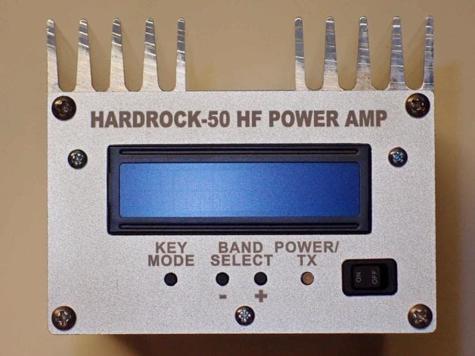
Click to zoom
Application Details
- Equipment Class
- AMP - Amplifier
- Date of Grant
- Nov 17, 2013
- Application Purpose
- Original Equipment
- Date of Application
- Jul 15, 2013
- Equipment Note
- 50W RF External Power Amplifier
- Frequency Range
- 1.80000000 - 21.45000000
- Company
- HobbyPCB, LLC
- Country
- United States
Documents & Files
Document Text
Text extracted from the exhibit documents filed with the FCC. Open a document above to read the original.
Users Manual
HARDROCK-50 USA Version Assembly Instructions Jim Veatch WA2EUJ June 30, 2012 TABLE OF CONTENTS 1. INTRODUCTION ..................................................................................................................................... 1 2. SPECIFICATIONS .................................................................................................................................... 2 3. ASSEMBLY OVERVIEW ........................................................................................................................... 3 4. CONTROL PCB INVENTORY .................................................................................................................... 4 1. REAR PANEL PCB INVENTORY ............................................................................................................... 5 2. AMPLIFIER PCB INVENTORY .................................................................................................................. 6 3. CHASSIS PACK INVENTORY .................................................................................................................... 8 4. FRONT PANEL PCB ............................................................................................................................... 10 5. BACK PANEL PCB ................................................................................................................................. 14 6. INDUCTORS AND TRANSFORMERS ..................................................................................................... 16 7. AMPLIFIER PCB .................................................................................................................................... 21 8. FINAL ASSEMBLY ................................................................................................................................. 29 9. ALIGNMENT PROCEDURE .................................................................................................................... 33 10. Chassis Wiring Diagram ....................................................................................................................... 37 11. AMPLIFIER PCB SCHEMATIC ................................................................................................................ 38 12. CONTROL PCB SCHEMATIC .................................................................................................................. 40 13. REAR PANEL PCB SCHEMATIC ............................................................................................................. 41 [1] 1. INTRODUCTION Congratulations on your purchase of a Hardrock-50 linear amplifier kit. The HR-50 is designed to provide 50W of RF power output with a drive level of 5 watts or less on the 160, 80, 40, 30, 20, 17 and 15 meter Amateur Radio frequency bands. The HR-50 is supplied as an easy to build kit that includes 3 printed circuit boards (PCBs), all necessary electrical and mechanical components and a rugged, professionally manufactured, aluminum enclosure. All surface mount components on the PCBs are installed using the latest pick and place technology and soldered with state of the art reflow equipment. The HR-50 is designed to provide higher power operation for low power analog and digital radios. Several interface options are available or under development for popular transceivers. Users are encouraged to customize the HR50 amplifier to meet their specific operating needs. Here is a list of possible modifications that licensed Amateur Radio operators have made to their HR-50 amplifiers: • Expanded frequency coverage to include 12, 10 and 6M Amateur Radio Bands (power output on 6M is 35W). • QSK circuit to replace the mechanical T/R relay with diode switching for extremely fast turn- around time. • Adding a second amplifier stage to lower drive requirements to the 0.5W input range to work with low power Software Defined radio kits. Building the HR-50 will be an excellent experience. The instructions have been thoroughly tested and updated with builder input to insure a successful build. Real time support is available from the entire HR-50 community at HobbyPCB.com/forums, seven days a week, 24 hours a day. And if for some reason you cannot get you amplifier going, contact me personally at [email protected] and I will personally make arrangements to fix your amplifier. The HR50 is designed to be rugged, both mechanically and electrically. The extruded aluminum case with 1/8” end panels is virtually indestructible, ready for backpacking or field day and laser etched labels and bright LCV display make the HR-50 look good in your home station as well. Electrically, the HR-50 is rated to operate in to any passive load from a dead short to open circuit and anywhere in between without reducing the output power, the input can withstand twice the rated input power indefinitely and power supply is tolerant to 16V. [2] 2. SPECIFICATIONS ITEM SPECIFICATION Frequency Range 160, 80, 40, 30, 20, 17, 15 meter Amateur Radio Bands Input Power 5W maximum Output Power 50W nominal DC Power 12-14 Volts, 10 Amps typical, 12A maximum Keying Modes Stand-by, Carrier Operated, Push-to-Talk Input/Output Jacks UHF Connectors Size 4.25” W by 3.5” H by 7.5” D (not including switches and connectors) Weight 2 lbs, 14 oz [3] 3. ASSEMBLY OVERVIEW Assembling the Hardrock-50 amplifier kit should be an enjoyable and rewarding experience. If at any time you feel frustrated or are having difficulty, take a break, ask questions on the forum or email, remember that if you are having a problem with something there’s a good chance that someone else has had the same issue. We have a “no questions asked” replacement part policy, so if you lose a part or need an extra length of wire of find something missing and email is all it will take to get you a replacement. The assembly is organized into the following subassemblies: • Front Paned PCB • Back Panel PCB • Inductors and Transformers • Ampl…
Text truncated - open the document above for the full version.
External Photos
HobbyPCB, LLC. Hardrock-50 External Photos Front: Rear: Top: Bottom: Left: Right:
External Photos
Document: Hardrock FCC Identifier: RHAHR50 Date: July 16, 2013 The following data is submitted with the application for type acceptance of the HobbyPCB, LLC. Hardrock-50 amplifier, FCC ID RHAHR50. We certify that device presented in the application. James C Veatch Curtis Pope Clearwater, Florida 33761 Hardrock-50 External Photos FCC Identifier: RHAHR50 The following data is submitted with the application for type acceptance of the HobbyPCB, LLC. ID RHAHR50. We certify that this information accurately represents the device presented in the application. HobbyPCB, LLC. 3373 E. Lake Shore Lane Clearwater, Florida 33761 The following data is submitted with the application for type acceptance of the HobbyPCB, LLC. represents the Clearwater, Florida 33761 Front: Rear: HobbyPCB, LLC. 3373 E. Lake Shore Lane Clearwater, Florida 33761 Clearwater, Florida 33761 Top: Bottom: HobbyPCB, LLC. 3373 E. Lake Shore Lane Clearwater, Florida 33761 Clearwater, Florida 33761 Left: Right: HobbyPCB, LLC. 3373 E. Lake Shore Lane Clearwater, Florida 33761
ID Label/Location Info
PART 2.1033 (c) (11) The following is a drawing of the equipment identification plate attached to an outer heatsink fin on the left side of each HobbyPCB Hardrock-‐50 amplifier:
ID Label/Location Info
Document: Hardrock FCC Identifier: RHAHR50 Date: July 16, 2013 The following data is submitted with the application for type acceptance of the HobbyPCB, LLC. Hardrock-50 amplifier, FCC represents the device presented in the application. James C Veatch Curtis Pope PART 2.1033 (c) (11) The following is a drawing of the equipment identification plate attached to an outer heatsink fin on the left side of each HobbyPCB Hardrock 3373 E. Lake Shore Lane Clearwater, Florida 33761 Hardrock-50 Label Drawing FCC Identifier: RHAHR50 Date: July 16, 2013 The following data is submitted with the application for type acceptance of the HobbyPCB, , FCC ID RHAHR50. We certify that this information accurately represents the device presented in the application. The following is a drawing of the equipment identification plate attached to an outer heatsink fin on the left side of each HobbyPCB Hardrock-50 amplifier: HobbyPCB, LLC. 3373 E. Lake Shore Lane Clearwater, Florida 33761 The following data is submitted with the application for type acceptance of the HobbyPCB, this information accurately The following is a drawing of the equipment identification plate attached to an outer
ID Label/Location Info
HobbyPCB, LLC. 3373 E. Lake Shore Lane Clearwater, Florida 33761 Document: Hardrock-50 Label Drawing FCC Identifier: RHAHR50 Date: Nov 9, 2013 The following data is submitted with the application for type acceptance of the HobbyPCB, LLC. Hardrock-50 amplifier, FCC ID RHAHR50. We certify that this information accurately represents the device presented in the application. James C Veatch Curtis Pope PART 2.1033 (c) (11) The following is a drawing of the equipment identification plate: The plate is attached to an outer heatsink fin on the left side of each HobbyPCB Hardrock-50 amplifier:
Internal Photos
HobbyPCB, LLC. Hardrock-50 Internal Photos (ribbon cable removed for visibility) Front: Rear: Left: Right:
Internal Photos
Document: Hardrock FCC Identifier: RHAHR50 Date: July 16, 2013 The following data is submitted with the application for type acceptance of the HobbyPCB, LLC. Hardrock-50 amplifier, FCC ID RHAHR50. We certify that device presented in the application. James C Veatch Curtis Pope Clearwater, Florida 33761 Hardrock-50 Internal Photos FCC Identifier: RHAHR50 The following data is submitted with the application for type acceptance of the HobbyPCB, LLC. ID RHAHR50. We certify that this information accurately represents the device presented in the application. HobbyPCB, LLC. 3373 E. Lake Shore Lane Clearwater, Florida 33761 The following data is submitted with the application for type acceptance of the HobbyPCB, LLC. represents the Clearwater, Florida 33761 Front: Rear: HobbyPCB, LLC. 3373 E. Lake Shore Lane Clearwater, Florida 33761 Clearwater, Florida 33761 Left: Right: HobbyPCB, LLC. 3373 E. Lake Shore Lane Clearwater, Florida 33761
Operational Description
HobbyPCB, LLC. Hardrock-50 FCC ID: RHAHR50 Operating Instructions: 1 – Set power switch to ‘ON’ position 2 – Press the Band + or – button to select the frequency band 3 – Select SB (Stand-by), CR (carrier operated) or PT (push to talk) keying mode Notes: In Stand-by mode or when the power switch is in the off position the RF input and RF output jacks are connected together and the Hardrock-50 amplifier is bypassed. When the Hardrock-50 amplifier is powered but not keyed, the LCD displays the selected band and operating mode, input voltage and heatsink temperature. When the Hardrock-50 amplifier is powered and keyed the LCD displays the average forward power, the peak envelope forward power, the reflected power and the calculated VSWR. Tune Up Procedure: 1. Select the proper band and operating mode on the Hardrock-50 amplifier and the exciter. 2. Adjust the output power level on the exciter not to exceed 5W into the Hardrock-50 amplifier and not to exceed 50W peak envelope forward power out of the Hardrock-50 amplifier.
Operational Description
Document: Hardrock- Procedures FCC Identifier: RHAHR50 Date: July 16, 2013 Operating Instructions: 1 – Set power switch to ‘ON’ position 2 – Press the Band + or – button to select the frequency band 3 – Select SB (Stand-by), CR (carrier operated) or PT (push to talk) keying mode Notes: In Stand-by mode or when the power switch is in the off position the RF input and RF output jacks are connected together and the Hardrock When the Hardrock-50 amplifier is powered but not keyed, the LCD displays the selected band and operating mode, input voltage and heatsink temperature. When the Hardrock-50 amplifier is powered and keyed the LCD displays the average forward power, the peak envelope forward power, the reflected power and the calculated VSWR. Tune Up Procedure: 1. Select the proper band and operating mode on the Hardrock exciter. 2. Adjust the output power level on the exciter not to exceed 5W into the Hardrock amplifier and not to exceed 50W peak envelope forward power out of the Hardrock amplifier. -50 Operating Instructions and Tune FCC Identifier: RHAHR50 Operating Instructions: Set power switch to ‘ON’ position button to select the frequency band CR (carrier operated) or PT (push to talk) keying mode by mode or when the power switch is in the off position the RF input and RF output jacks are connected together and the Hardrock-50 amplifier is bypassed. 50 amplifier is powered but not keyed, the LCD displays the and operating mode, input voltage and heatsink temperature. 50 amplifier is powered and keyed the LCD displays the average forward power, the peak envelope forward power, the reflected power and the Select the proper band and operating mode on the Hardrock-50 amplifier and the 2. Adjust the output power level on the exciter not to exceed 5W into the Hardrock amplifier and not to exceed 50W peak envelope forward power out of the Hardrock HobbyPCB, LLC. 3373 E. Lake Shore Lane Clearwater, Florida 33761 Operating Instructions and Tune-up CR (carrier operated) or PT (push to talk) keying mode by mode or when the power switch is in the off position the RF input and RF 50 amplifier is bypassed. 50 amplifier is powered but not keyed, the LCD displays the and operating mode, input voltage and heatsink temperature. 50 amplifier is powered and keyed the LCD displays the average forward power, the peak envelope forward power, the reflected power and the 50 amplifier and the 2. Adjust the output power level on the exciter not to exceed 5W into the Hardrock-50 amplifier and not to exceed 50W peak envelope forward power out of the Hardrock-50
Parts List/Tune Up Info
HobbyPCB, LLC. Hardrock-50 RHAHR50 PARTS LIST ITEM QTY REFERENCE DESIGNATOR DESCRIPTION 1 33 C1,C2,C3,C4,C6,C9,C11,C13,C14,C15,C16,C17,C1 8,C19,C20,C24,C25,C26,C28,C29,C32,C37,C44,C4 5,C46,C56,C57,C103,C104,C105,C106,C113,C114 CAPAXCITOR CER 0.1UF, 100V, X7R, 1206 2 4 C101, C102,C303,C304 CAPACITOR CER 22PF 630V, C0G, 1206 3 2 C12,C30 CAPACITOR CER 68PF 200V, C0G, 1206 4 1 C302 CAPACITOR 1206, X7R, 10V, 470NF 5 2 C34,C35, C301 CAPACITOR CER 1UF, 25V, X7R, 20%, 1206 6 1 C35 CAPACITOR, TANTALUM, 1206, 16V, 1 UF 7 2 C39,C58 CAPACITOR CER 220PF 630V 5% NP0 8 2 C40,C38 CAPACITOR CER 100PF 630V 5% NP0 9 3 C41,C43, C53 CAPACITOR CER 150PF 630V 5% NP0 10 1 C42 CAPACITOR CER 270PF 630V 5% NP0 1206 11 1 C48 CAPACITOR CER 680PF 630V 5% NP0 1206 12 2 C49,C47 CAPACITOR CER 330PF 630V NPO 5% 1206 13 3 C5,C21,C31 CAPACITOR CER 4700PF 200V, X7R, 1206 14 1 C51 CAPACITOR CER 1000PF 630V 5% NP0 15 2 C52,C50 CAPACITOR CER 560PF 630V 5% NP0 16 2 C55,C54 CAPACITOR CER 1800PF 630V 5% NP0 1206 17 2 C59,C60 CAPACITOR CER 3300PF 630V 10% X7R 1206 18 2 C7,C33 CAPACITOR CER 1500PF 200V, NPO, 1206 19 4 C8,C36,C112,C306 CAPACITOR TANT 10UF 16V 10% SMD 20 1 CHASSIS 2 PIECE ALUM EXTR, ENDPLTS, HARDWARE 21 1 CONTROL CABLE 30CM IDC-10 CABLE 22 5 D1,D3,D4,D101, D102 DIODE, 100V 150mA SOD-323 23 1 D105 3MM BI-COLOR LED 24 1 D2 ZENER DIODE, 200mW, 5.1V, SOD-323 25 2 DC POWER CONTACT POWERPOLE 15AMP CONTACT #16-#20 WIRE 26 1 DC POWER HOUSING POWERPOLE PP15 BLK/RED HOUSING #1327G6 27 1 DRIVER POWER CONNECTOR MOLEX 22-01-3037 28 1 DRIVER POWER HEADER MOLEX 22-23-2031 29 14 FB1,FB2,FB3,FB4,FB5,FB6,FB7,FB8,FB9,FB10,FB1 1,FB12,FB13, FB301 FERRITE BEAD, SMD, 1kohm, 500mA 30 2 GND,13VDC 1/4" SPADE TERMINAL PCB MOUNT 31 1 IC102 IC, LDO REGULATOR 5.0V 0.8A 32 1 IC301 IC, MCP2200 USB SW, 12MBPS, SSOP-20 33 1 J1 DUAL ROW 20-PIN HEADER RA 34 2 JP101, JP302 DUAL ROW 10 PIN HEADER VERT 35 1 JP102 SINGLE ROW 16 PIN HEADER VERT 36 4 L1,L2,L3,L4 INDUCTOR POWER 0.068UH 1008 37 4 L13,L12,L14,L15 T50-2 CORE WITH #22 ENAMELED WIRE 38 4 L5, T1, T3, T201 CORE TYPE 43 WITH TEFLON WIRE 39 4 L9,L8,L11,L10 T50-6 CORE WITH #22 ENAMELED WIRE 40 1 LCD101 LCD MODULE 2X16 WITH BACKLIGHT 41 1 PCB AMPLIFIER PCB 2 SIDES 2 OZ. CU 42 1 PCB FRONT PANEL PCB 2 SIDES 2 OZ. CU 43 1 PCB REAR PANEL PCB 2 SIDES 2 OZ. CU 44 10 PINS FOR DRIVER CABLING MOLEX 08-50-0114 45 4 Q1,Q2,Q3,Q4 RD16HHF1 MOSFET RF 16W TO-220 46 1 Q5 TRANSISTOR, NPN, 40V, 200MA, 3-SOT-23 47 2 Q6, Q101 2N7002, MOSFET, 25V, 220mA SOT-23 48 4 R1,R2,R3,R4 RES, 49.9OHM, 500mW, 1% 49 8 R103, R104, R115, R116, R117, R118, R119, R301 RES, 1K OHM, 125mW, 1% 50 2 R11,R10 RES, 470OHM, 1W, 5%, 2512 51 1 R111 TRIMPOT VERT ADJ 10K 1T 52 4 R13,R14,R15,R16 RES, 100OHM, 330mW, 1%, 1210 53 1 R22 RES, 1.5KOHM, 250mW, 1%, 1206 54 10 R5,R7,R17,R18,R19,R20,R21,R23,R112,R113 RES 470 OHM 1/4W 1% 1206 55 11 R6,R12,,R101, R102, R105, R106, R107, R108, R109, R110, R114 RES, 1206, 10KOHM, 125mW, 1% 56 2 R8,R9 RES 100K OHM 1/4W 1% 1206 57 2 RF_IN, RF_OUT CONNECTOR MOLEX 22-01-3027 58 2 RF_IN, RF_OUT HEADER MOLEX 22-23-2021 59 1 RLY1 RELAY DPDT 5A 12V COIL 60 14 RLY2,RLY3,RLY4,RLY5,RLY6,RLY7,RLY8,RLY9,RLY1 0,RLY11,RLY12,RLY13,RLY14,RLY15 RELAY DPDT 2A 12V COIL 61 3 S101, S102, S103 SWITCH, PB, PCB MOUNT 62 1 SW1 SWITCH, ROCKER, SPST, 3A, 250V, BLACK 63 1 T2 T75-43 RF BALUN 16:1 64 1 U1 IC, LDO VOLT REG, 5V, 0.1A, 8-SOIC 65 1 U100 IC, PIC 18F45K22 TQFP 44-PIN 66 1 U2 LM35, IC, TEMP SENSOR, TO-92-3 67 1 U3 IC, RELAY DRIVER, NPN, 8, 50V, 68 2 UHF Panel Connector RF IN, RF OUT CONNECTOR 69 4 VR1,VR2,VR3,VR4 TRIMPOT VERT ADJ 1K 25T 70 1 X302 9 PIN PCB MOUNT SUB-D 71 1 X303 USB CONNECTOR 72 1 Y301 12MHX CRYSTAL
Parts List/Tune Up Info
Document: Hardrock-50 FCC Identifier: RHAHR50 Date: July 16, 2013 The following data is submitted with the application for type acceptance of the HobbyPCB, LLC. Hardrock amplifier, FCC ID RHAHR50. We certify that application. James C Veatch Curtis Pope 50 Parts List FCC Identifier: RHAHR50 The following data is submitted with the application for type acceptance of the HobbyPCB, LLC. Hardrock ID RHAHR50. We certify that this information accurately represents the device presented in the HobbyPCB, LLC. 3373 E. Lake Shore Lane Clearwater, Florida 33761 The following data is submitted with the application for type acceptance of the HobbyPCB, LLC. Hardrock-50 represents the device presented in the ITEM QTY REFERENCE DESIGNATOR 1 33 C1,C2,C3,C4,C6,C9,C11,C13,C14,C15,C16,C17,C1 8,C19,C20,C24,C25,C26,C28,C29,C32,C37,C44,C4 5,C46,C56,C57,C103,C104,C105,C106,C113,C114 2 4 C101, C102,C303,C304 3 2 C12,C30 4 1 C302 5 2 C34,C35, C301 6 1 C35 7 2 C39,C58 8 2 C40,C38 9 3 C41,C43, C53 10 1 C42 11 1 C48 12 2 C49,C47 13 3 C5,C21,C31 14 1 C51 15 2 C52,C50 16 2 C55,C54 17 2 C59,C60 18 2 C7,C33 19 4 C8,C36,C112,C306 20 1 CHASSIS 21 1 CONTROL CABLE 22 5 D1,D3,D4,D101, D102 23 1 D105 24 1 D2 25 2 DC POWER CONTACT 26 1 DC POWER HOUSING 27 1 DRIVER POWER CONNECTOR 28 1 DRIVER POWER HEADER 29 14 FB1,FB2,FB3,FB4,FB5,FB6,FB7,FB8,FB9,FB10,FB1 1,FB12,FB13, FB301 30 2 GND,13VDC 31 1 IC102 32 1 IC301 33 1 J1 34 2 JP101, JP302 35 1 JP102 REFERENCE DESIGNATOR DESCRIPTION C1,C2,C3,C4,C6,C9,C11,C13,C14,C15,C16,C17,C1 8,C19,C20,C24,C25,C26,C28,C29,C32,C37,C44,C4 5,C46,C56,C57,C103,C104,C105,C106,C113,C114 CAPAXCITOR CER 0.1UF, 100V, CAPACITOR CER 22PF 630V, C0G, 1206 CAPACITOR CER 68PF 200V, C0G, 1206 CAPACITOR 1206, X7R, 10V, 470NF CAPACITOR CER 1UF, 25V, X7R, 20%, 1206 CAPACITOR, TANTALUM, 1206, 16V, 1 UF CAPACITOR CER 220PF 630V 5% NP0 CAPACITOR CER 100PF 630V 5% NP0 CAPACITOR CER 150PF 630V 5% NP0 CAPACITOR CER 270PF 630V 5% NP0 1206 CAPACITOR CER 680PF 630V 5% NP0 1206 CAPACITOR CER 330PF 630V NPO 5% 1206 CAPACITOR CER 4700PF 200V, X7R, 1206 CAPACITOR CER 1000PF 630V 5% NP0 CAPACITOR CER 560PF 630V 5% NP0 CAPACITOR CER 1800PF 630V 5% CAPACITOR CER 3300PF 630V 10% X7R 1206 CAPACITOR CER 1500PF 200V, NPO, 1206 CAPACITOR TANT 10UF 16V 10% SMD 2 PIECE ALUM EXTR, ENDPLTS, HARDWARE 30CM IDC-10 CABLE DIODE, 100V 150mA SOD 3MM BI-COLOR LED ZENER DIODE, 200mW, 5.1V, SOD POWERPOLE 15AMP CONTACT #16 POWERPOLE PP15 BLK/RED HOUSING #1327G6 DRIVER POWER CONNECTOR MOLEX 22-01-3037 MOLEX 22-23-2031 FB1,FB2,FB3,FB4,FB5,FB6,FB7,FB8,FB9,FB10,FB1FERRITE BEAD, SMD, 1kohm, 500mA 1/4" SPADE TERMINAL PCB MOUNT IC, LDO REGULATOR 5.0V 0.8A IC, MCP2200 USB SW, 12MBPS, SSOP DUAL ROW 20-PIN HEADER RA DUAL ROW 10 PIN HEADER VERT SINGLE ROW 16 PIN HEADER VERT HobbyPCB, LLC. 3373 E. Lake Shore Lane Clearwater, Florida 33761 CAPAXCITOR CER 0.1UF, 100V, X7R, 1206 CAPACITOR CER 22PF 630V, C0G, 1206 CAPACITOR CER 68PF 200V, C0G, 1206 CAPACITOR 1206, X7R, 10V, 470NF CAPACITOR CER 1UF, 25V, X7R, 20%, 1206 CAPACITOR, TANTALUM, 1206, 16V, 1 UF CAPACITOR CER 220PF 630V 5% NP0 CAPACITOR CER 100PF 630V 5% NP0 CAPACITOR CER 150PF 630V 5% NP0 CAPACITOR CER 270PF 630V 5% NP0 1206 630V 5% NP0 1206 CAPACITOR CER 330PF 630V NPO 5% 1206 CAPACITOR CER 4700PF 200V, X7R, 1206 CAPACITOR CER 1000PF 630V 5% NP0 CAPACITOR CER 560PF 630V 5% NP0 CAPACITOR CER 1800PF 630V 5% NP0 1206 CAPACITOR CER 3300PF 630V 10% X7R 1206 CAPACITOR CER 1500PF 200V, NPO, 1206 CAPACITOR TANT 10UF 16V 10% SMD 2 PIECE ALUM EXTR, ENDPLTS, HARDWARE DIODE, 100V 150mA SOD-323 ZENER DIODE, 200mW, 5.1V, SOD-323 POWERPOLE 15AMP CONTACT #16-#20 WIRE POWERPOLE PP15 BLK/RED HOUSING #1327G6 FERRITE BEAD, SMD, 1kohm, 500mA 1/4" SPADE TERMINAL PCB MOUNT REGULATOR 5.0V 0.8A IC, MCP2200 USB SW, 12MBPS, SSOP-20 PIN HEADER RA DUAL ROW 10 PIN HEADER VERT SINGLE ROW 16 PIN HEADER VERT 36 4 L1,L2,L3,L4 37 4 L13,L12,L14,L15 38 4 L5, T1, T3, T201 39 4 L9,L8,L11,L10 40 1 LCD101 41 1 PCB AMPLIFIER 42 1 PCB FRONT PANEL 43 1 PCB REAR PANEL 44 10 PINS FOR DRIVER CABLING 45 4 Q1,Q2,Q3,Q4 46 1 Q5 47 2 Q6, Q101 48 4 R1,R2,R3,R4 49 8 R103, R104, R115, R116, R117, R118, R119, R301 50 2 R11,R10 51 1 R111 52 4 R13,R14,R15,R16 53 1 R22 54 10 R5,R7,R17,R18,R19,R20,R21,R23,R112,R113 55 11 R6,R12,,R101, R102, R105, R106, R107, R108, R109, R110, R114 56 2 R8,R9 57 2 RF_IN, RF_OUT CONNECTOR 58 2 RF_IN, RF_OUT HEADER 59 1 RLY1 60 14 RLY2,RLY3,RLY4,RLY5,RLY6,RLY7,RLY8,RLY9,RLY1 0,RLY11,RLY12,RLY13,RLY14,RLY15 61 3 S101, S102, S103 62 1 SW1 63 1 T2 64 1 U1 65 1 U100 66 1 U2 67 1 U3 68 2 UHF Panel Connector 69 4 VR1,VR2,VR3,VR4 70 1 X302 71 1 X303 72 1 Y301 INDUCTOR POWER 0.068UH 1008 T50-2 CORE WITH #22 ENAMELED WIRE CORE TYPE 43 WITH TEFLON WIRE T50-6 CORE WITH #22 ENAMELED WIRE LCD MODULE 2X16 WITH BACKLIGHT PCB 2 SIDES 2 OZ. CU PCB 2 SIDES 2 OZ. CU PCB 2 SIDES 2 OZ. CU PINS FOR DRIVER CABLING MOLEX 08-50-0114 RD16HHF1 MOSFET RF 16W TO TRANSISTOR, NPN, 40V, 200MA, 3 2N7002, MOSFET, 25V, 220mA SOT RES, 49.9OHM, 500mW, 1% R103, R104, R115, R116, R117, R118, R119, RES, 1K OHM, 125mW, 1% RES, 470OHM, 1W, 5%, 2512 TRIMPOT VERT ADJ 10K 1T RES, 100OHM, 330mW, 1%, 1210 RES, 1.5KOHM, 250mW, 1%, 1206 R5,R7,R17,R18,R19,R20,R21,R23,R112,R113 RES 470 OHM 1/4W 1% 1206 R6,R12,,R101, R102, R105, R106, R107, R108, RES, 1206, 10KOHM, 125mW, 1% RES 100K OHM 1/4W 1% 1206 RF_IN, RF_OUT CONNECTOR MOLEX 22-01-3027 MOLEX 22-23-2021 RELAY DPDT 5A 12V COIL RLY2,RLY3,RLY4,RLY5,RLY6,RLY7,RLY8,RLY9,RLY1 0,RLY11,RLY12,RLY13,RLY14,RLY15 RELAY DPDT 2A 12V COIL SWITCH, PB, PCB MOUNT SWITCH, ROCKER, SPST, 3A, 250V, BLACK T75-43 RF BALUN 16:1 IC, LDO VOLT REG, 5V, 0.1A, 8 IC, PIC 18F45K22 TQFP 44 LM35, IC, TEMP SENSOR, TO IC, RELAY DRIVER, NPN, 8, 50V, RF IN, RF OUT CONNECTOR TRIMPOT VERT ADJ 1K 25T 9 PIN PCB MOUNT SUB-D USB CONNECTOR 12MHX CRYSTAL HobbyPCB, LLC. 3373 E. Lake Shore Lane Clearwater, Florida 33761 INDUCTOR POWER 0.068UH 1008 2 CORE WITH #22 ENAMELED WIRE CORE TYPE 43 WITH TEFLON WIRE 6 CORE WITH #22 ENAMELED WIRE LCD MODULE 2X16 WITH BACKLIGHT RD16HHF1 MOSFET…
Text truncated - open the document above for the full version.
Schematics
1. AMPLIFIER PCB SCHEMATIC Amplifier PCB Schematic Page 1 Amplifier PCB Schematic Page 2: 2. CONTROL PCB SCHEMATIC 3. REAR PANEL PCB SCHEMATIC 4. Chassis Wiring Diagram 50W AMP PCBCONTROL PCB 20 PIN HEADER M/F DIRECT CONNECTION REAR PANEL PCB 10 PIN IDC CABLE REAR PANEL PK RG-174 COAX CHASSIS PK RG-174 COAX CHASSIS PK RCA JACK RF_IN RCA JACK RF_OUT RCA PLUG RCA PLUG UHF JACK UHF JACK INPUTOUTPUT RCA JACK DB-9USB PTTACCUSB REAR PANEL POWER POLE 13 VDC GND 1/4" SPADE TERMINALS POWER DIRECT SOLDER RLY_OUT 2X #18 WIRE 2 PIN MOLEX 2 PIN HDR AMP_IN 2 PIN MOLEX 2 PIN HDR PWRSW RG-174 COAX POWER SW 2X #22 WIRE CHASSIS PK CONNECT RLY_OUT TO AMP_IN IF DRIVER PCB NOT PRESENT CABLE ASSEMBLY CHASSIS PK
Schematics
Document: Hardrock FCC Identifier: RHAHR50 Date: July 16, 2013 The following data is submitted with the application for type acceptance of the HobbyPCB, LLC. Hardrock-50 amplifier, FCC ID RHAHR50. We certify that device presented in the application. James C Veatch Curtis Pope Clearwater, Florida 33761 Hardrock-50 Schematic/Wiring Diagrams FCC Identifier: RHAHR50 The following data is submitted with the application for type acceptance of the HobbyPCB, LLC. ID RHAHR50. We certify that this information accurately represents the device presented in the application. HobbyPCB, LLC. 3373 E. Lake Shore Lane Clearwater, Florida 33761 Schematic/Wiring Diagrams The following data is submitted with the application for type acceptance of the HobbyPCB, LLC. represents the 1. AMPLIFIER PCB SCHEMATIC Amplifier PCB Schematic Page 1 Clearwater, Florida 33761 AMPLIFIER PCB SCHEMATIC HobbyPCB, LLC. 3373 E. Lake Shore Lane Clearwater, Florida 33761 Amplifier PCB Schematic Page 2: Clearwater, Florida 33761 Amplifier PCB Schematic Page 2: HobbyPCB, LLC. 3373 E. Lake Shore Lane Clearwater, Florida 33761 2. CONTROL PCB SCHEMATIC Clearwater, Florida 33761 CONTROL PCB SCHEMATIC HobbyPCB, LLC. 3373 E. Lake Shore Lane Clearwater, Florida 33761 3. REAR PANEL PCB SCHEMATIC Clearwater, Florida 33761 REAR PANEL PCB SCHEMATIC HobbyPCB, LLC. 3373 E. Lake Shore Lane Clearwater, Florida 33761 4. Chassis Wiring Diagram RG-174 COAX RCA JACK RF_IN RCA PLUG UHF JACK INPUT POWER POLE 13 VDC GND 1/4" SPADE TERMINALS POWER DIRECT SOLDER RLY_OUT 2X #18 WIRE RG-174 COAX CONNECT RLY_OUT TO AMP_IN IF DRIVER PCB NOT PRESENT CABLE ASSEMBLY CHASSIS PK Clearwater, Florida 33761 Chassis Wiring Diagram 50W AMP PCB 20 PIN HEADER M/F DIRECT CONNECTION REAR PANEL PCB RG-174 COAX CHASSIS PK RG-174 COAX CHASSIS PK RCA JACK RF_IN RCA JACK RF_OUT RCA PLUG UHF JACK INPUTOUTPUT DB-9 ACC REAR PANEL 13 VDC DIRECT SOLDER RLY_OUT 2 PIN MOLEX 2 PIN HDR AMP_IN 2 PIN MOLEX 2 PIN HDR PWRSW COAX 2X #22 WIRE CHASSIS PK HobbyPCB, LLC. 3373 E. Lake Shore Lane Clearwater, Florida 33761 CONTROL PCB REAR PANEL PCB 10 PIN IDC CABLE REAR PANEL PK RCA JACK USB PTTUSB POWER SW 2X #22 WIRE CHASSIS PK
Test Report
FCC Test Report HobbyPCB Model Hardrock-50 50W RF External Power Amplifier The following sections of CFR Title 47: Telecommunication apply to the DUT and are included in this report: • 2.1033 Application for certification. • 2.1046(a) Measurements required: RF power output. • 2.815 External radio frequency power amplifiers. • 97.307(d) Emission standards. • 97.313 Transmitter power standards. • 97.315 Certification of external RF power amplifiers. • 97.317 Standards for certification of external RF power amplifiers. 3373 E. Lake Shore Lane Clearwater, Florida 33761 FCC ID: RHA-HR50 Tested by: James Veatch Date: July 3, 2031 Test Results: The HobbyPCB Hardrock-50 50W RF External Amplifier has been tested and passed and therefore meets the requirements of each FCC section listed above. Table of Contents 1.0 General Information .......................................................................................................................................3 2.0 Attestation Statement ....................................................................................................................................4 3.0 Other Information ..........................................................................................................................................5 4.0 PART 97.313....................................................................................................................................................5 5.0 PART 2.1033 (c) (8) .........................................................................................................................................5 6.0 PART 2.1033 (c) (11) .......................................................................................................................................5 7.0 PART 2.815 (b) (1) (2) .....................................................................................................................................6 8.0 Test Setup and Conditions ..............................................................................................................................6 9.0 Test Equipment List ........................................................................................................................................7 10.0 Test Procedures ..............................................................................................................................................9 10.1 The Elecraft K2 Exciter ....................................................................................................................................9 10.2 Calibrating the Attenuator .............................................................................................................................9 10.3 Gain and Spurious Emissions Tests .............................................................................................................. 10 10.4 Test Frequencies .......................................................................................................................................... 12 11.0 Test Results .................................................................................................................................................. 13 11.1 Attenuator Test Results ............................................................................................................................... 13 11.2 Gain Test Results ......................................................................................................................................... 13 11.2 Spurious Emissions Test Results .................................................................................................................. 14 1.0 General Information Device Under Test: 50W HF Linear Power Am…
Text truncated - open the document above for the full version.
Contact Information
Applicant
Curtis Pope(Manager)
Technical Specifications
| # | Rule Parts | Frequency Range | Power Output | Emission |
|---|---|---|---|---|
| 1 | 97 | 1.8 MHz - 21.45 MHz | 50 W | A1A |