S7A-SP11910S
Sena Technologies Co., Ltd.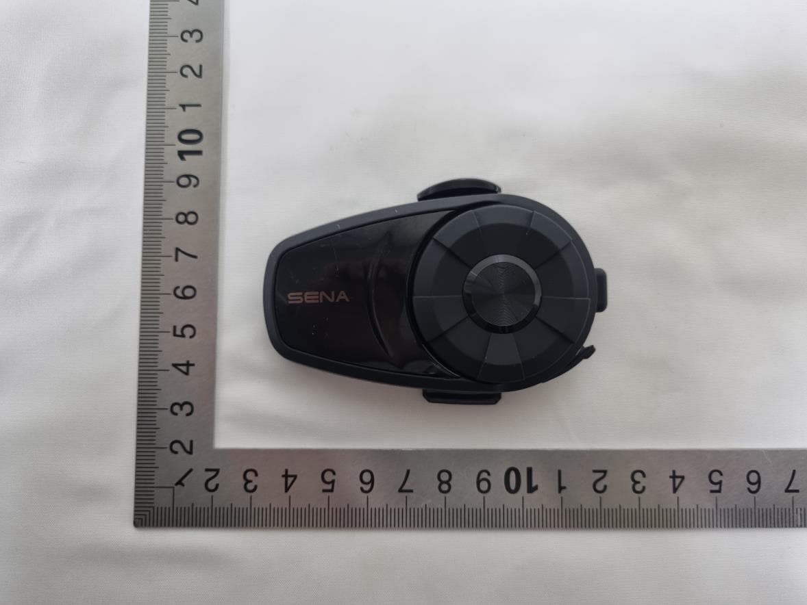
Click to zoom
Application Details
- Equipment Class
- DSS - Part 15 Spread Spectrum Transmitter
- Date of Grant
- Dec 21, 2022
- Application Purpose
- Original Equipment
- Date of Application
- Dec 21, 2022
- Equipment Note
- 10S
- Frequency Range
- 2402.00000000 - 2480.00000000
- Company
- Sena Technologies Co., Ltd.
- Country
- South Korea
Documents & Files
Document Text
Text extracted from the exhibit documents filed with the FCC. Open a document above to read the original.
Users Manual
10S Manual Charging Red LED: Charging Blue LED: Fully charged Power On/Off Press and hold the Jog Dial and Phone Button for 1 second Tap the Jog Dial and Phone Button. Volume Adjustment Increase/Decrease the volume : Rotate the Jog Dial clockwise or counterclockwise Battery Check Phone, Music Pairing Initially Pairing the headset The headset will automatically enter the phone pairing mode when you initially turn on the headset or in the following situation: • Rebooting after executing Factory Reset 1. Press and hold the Jog Dial and Phone Button for 1 second. 2. Search for Bluetooth devices on your mobile phone. Select the headset in the list of the devices detected on the mobile phone. 3. Enter 0000 for the PIN. Some mobile phones may not ask for the PIN. Music Operation Play or pause music: Press and hold the Jog Dial for 1 second. Track forward/ back: Rotate while pressing the Jog Dial clockwise or counterclockwise. Mobile Phone Call Making and Answering Answering a call: Tap the Phone Button Ending a call: Tap the Phone Button Voice dial: Tap the Phone Button Speed dial: Double tap the Phone Button Rejecting a call: Press and hold the Jog Dial for 2 seconds. Intercom Intercom Pairing 1. Press and hold the Jog Dial of two headsets for 5 seconds until red LEDs of both units start to flash rapidly. 2. Simply tap the Jog Dial of any one of the two headsets. Intercom Start/End : Tap the Jog Dial. Setting Configuration Menu: Press the Jog Dial for 10 seconds. Using the Sena Device Manager Connect the headset to your computer via a USB cable. Launch the Sena Device Manager and click DEVICE SETTING to configure the headset settings. For details about downloading the Sena Device Manager, please refer to the leaflet included in the package. Troubleshooting Factory Reset If you want to restore the headset to factory default settings, Press and hold the Phone Button for 10 seconds and tap the Jog Dial . The headset automatically restores the default settings and turns off. Certification and Safety Approvals FCC Compliance Statement This device complies with part 15 of the FCC rules. Operation is subject to the following two conditions: (1) This device may not cause harmful interference, and (2) This device must accept any interference received, including interference that may cause undesired operation. This equipment has been tested and found to comply with the limits for a Class B digital device pursuant to part 15 of the FCC rules. These limits are designed to provide reasonable protection against harmful interference in a residential installation. This equipment generates, uses and can radiate radio frequency energy and, if not installed and used in accordance with the instructions, may cause harmful interference to radio communications. However, there is no guarantee that interference will not occur in a particular installation. If this equipment does cause harmful interference to radio or television reception, which can be determined by turning the equipment on and off, the user is encouraged to try to correct the interference by one or more of the following measures: -Reorient or relocate the receiving antennae -Increase the separation between the equipment and the receiver -Connect the equipment into an outlet on a circuit different from that to which the receiver is connected. -Consult the dealer or an experienced radio/TV technician for help. FCC RF Exposure Statement This equipment complies with FCC radiation exposure limits set forth for an uncontrolled environment. End users must follow the specific operating instructions for satisfying RF exposure compliance. The antenna used for this transmitter must not transmit simultaneously with any other antenna or transmitter, except in accordance with FCC multi-transmitter product procedures. When equipped, the distance between antenna and one’s head surface is 40mm. FCC Caution Any changes or modifications to the equipment not expressly approved by the party responsible for compliance could void user’s authority to operate the equipment. Certification et homologation de sécurité Déclaration de conformité FCC Cet appareil est en conformité avec la partie 15 des règles de la FCC. Son fonctionnement est soumis aux deux conditions suivantes : (1) Cet appareil ne doit pas créer d’interférences préjudiciables et (2) Cet appareil doit accepter toutes les interférences reçues, y compris celles qui pourraient entraver son bon fonctionnement. Cet équipement a été testé et jugé conforme aux limites pour un appareil numérique de classe B, conformément à la partie 15 des règles de la FCC. Ces limites sont conçues pour fournir une protection raisonnable contre les interférences nuisibles dans une installation résidentielle. Cet équipement génère et utilise de l’énergie radio fréquence et, s’il n’est pas installé et utilisé conformément. aux instructions, il peut occasionner des interférences nuisibles au niveau des communications radios. Cependant, il n’existe aucune garantie que ces interférences ne se produiront pas dans une installation particulière. Si cet équipement génère des interférences nuisibles à la réception de la radio ou de la télévision (ce qu’il est possible de déterminer en mettant l’équipement hors tension, puis sous tension), l’utilisateur est invité à suivre une ou plusieurs des mesures suivantes pour corriger le problème des interférences en prenant l’une des mesures suivantes : -Modifier l’emplacement ou l’orientation de l’antenne de réception. -É loigner l’appareil du récepteur. -Brancher l’appareil sur une prise située sur un circuit différent de celui du récepteur. -Consulter le revendeur ou un technicien expérimenté pour obtenir de l’aide. É noncé FCC sur l’exposition aux radiations RF Cet équipement est conforme aux réglementations FCC d’exposition aux radiations définies pour un environnement non contrôlé. Les utilisateurs doivent respecter les instructions d’exploitation spécifiques pour répondre aux exigences de conformité s…
Text truncated - open the document above for the full version.
Attestation Statements
SENA TECHNOLOGIES.Inc December 14, 2022 Applicant: SENA TECHNOLOGIES.Inc FCC ID: S7A-SP119 / IC: 8154A-SP119 To. Whom it may concern: We, Sena Technologies,Inc. declare that when equipped, the distance between antenna and one’s head surface is 40mm. Seunghyun Kim, Research Engineer
Cover Letter(s)
SENA TECHNOLOGIES.Inc 19, Heolleung-ro 569-gil, Gangnam-gu, Seoul, South Korea Federal Communications Commission Authorization and Evaluation Division Confidentiality Request regarding application for certification of FCC ID: S7A-SP119 Pursuant to Sections 0.457 and 0.459 of the Commission’s Rules, we hereby request confidential treatment of information accompanying this application as outlined below: Exhibit Type File Name Block Diagram Schematics Operational Description Part List [SP119] BLK [SP119] SCH [SP119] OpDes [SP119] Part List The above materials contain trade secrets and proprietary information not customarily released to the public. The public disclosure of these materials may be harmful to the applicant and provide unjustified benefits to its competitors. The applicant understands that pursuant to Section 0.457 of the Rules, disclosure of this application and all accompanying documentation will not be made before the date of the Grant for this application. In additional to above mentioned documents, in order to comply with the marketing regulations in Title 47 CFR §2.803 and the importation rules in Title 47 CFR §2.1204, while ensuring that business sensitive information remains confidential until the actual marketing of newly authorized devices, we request Short Term Confidentiality of the following attachment(s); Exhibit Type File Name External Photos Internal Photos Test Setup Photos Manual [SP119] EXT Photo [SP119] INT Photo [SP119] Test Setup Photo [SP119] Manual For 45 days, pursuant to Public Notice DA 04-1705. OR For 180 days pursuant to KDB 726920 D01. Sincerely, Seunghyun KIM / Research Engineer
Cover Letter(s)
SENA TECHNOLOGIES.Inc 19, Heolleung-ro 569-gil, Gangnam-gu, Seoul, South Korea Dec 19, 2022 FEDERAL COMMUNICATIONS COMMISSIONS Authorization and Evaluation Division 7435 Oakland Mills Road Columbia, MD 21046 Letter of Authorization We, the undersigned, hereby authorize Yong-Min, Won of EMC Labs Co., Ltd. to act on our behalf in all manners relating to application for equipment authorization for FCC ID: S7A-SP119 / IC: 8154A-SP119 including signing of all documents relating to these matters. Any and all acts carried out by Yong-Min, Won of EMC Labs Co., Ltd. on our behalf shall have the same affect as acts of our own. This authorization is valid until further written notice from SENA TECHNOLOGIES.Inc “I, the undersigned, hereby certify that we are not subject to a denial of federal benefits, that includes FCC benefits, pursuant to Section 5301 of the Anti-Drug Abuse Act of 1988, 21 U.S.C. 853(a).” Sincerely, Seunghyun KIM / Research Engineer
External Photos
USB Port (Type C _ Charging Only)
ID Label/Location Info
SENA_SP119_Label & Location Label Location (Rear)
Internal Photos
Internal BT Antenna
RF Exposure Info
Model Name : FCC ID : (mm)(dBm)(dB)(dBm)(mW) 240216.8217.3253.953.00PASS 244117.0917.5957.413.00PASS 248016.8217.3253.953.00PASS 24027.187.685.863.00PASS 24417.688.186.583.00PASS 24807.317.816.043.00PASS 24027.928.426.953.00PASS 24418.398.897.743.00PASS 24808.048.547.143.00PASS 24021.762.261.683.00PASS 24422.513.012.003.00PASS 24802.102.601.823.00PASS S7A-SP119Separation distance : 40.0 mm MPE Calculation KDB 447498 - 4.3.1 a) For 100 MHz to 6 GHz and test separation distances ≤ 50 mm, the 1-g and 10-g SAR test exclusion thresholds are determined by the following: [(max. power of channel, including tune-up tolerance, mW) / (min. test separation distance, mm)] · [√f(GHz)] ≤ 3.0 for 1-g SAR, and ≤ 7.5 for 10-g extremity SAR, where - f(GHz) is the RF channel transmit frequency in GHz - Power and distance are rounded to the nearest mW and mm before calculation - The result is rounded to one decimal place for comparison SP119Device Category : Portable device Standalone SAR Test exclusion thresholds for 100MHz to 6GHz at test separation distance ≤ 50 mm LimitResult GFSK 40.00± 0.50 2.0904 2.2425 2.1241 Modulation Frequency (MHz) Min. Test separation distance Measured Maximum Average power Tune-up tolerance Max. Power with tune-up tolerance π/4DQPSK 40.00± 0.50 0.2271 0.2569 0.2378 8DPSK 40.00± 0.50 0.2693 0.3025 0.2813 BT LE 40.00± 0.50 0.0652 0.0781 0.0716
Test Report
SPECIFICA TION Chip Antenna Model No. : SENA_003 WRITTEN CHECKED APPROVED Seunghyun Kim Seunghyun Kim July 22, 2009 Notes The content s of this data sheet are subject to change without notice. Please confirm the specifications and delivery conditions when placing your order. - 2 - CHIP ANTENNA 1. SPECIFICATIONS 1.1. Electrical Specifications ITEM SPEC. Unit Frequency 2400-2485 MHz Bandwidth @ VSWR 2.5:1 100 MHz Gain Max. 0.3dBi Polarization Linear Azimuth Beam Pattern Omni-directional Impedance 50 Ω ※ These values are measured on the matched reference test board. 1.2. Mechanical Specifications Electrode Silver Dimensions (L x W x H) 9.0 x 3.0 x 1.2 mm Operating Temperature -35 ~ +85 °C 1.3. Appearance and Dimensions L 9.0 W 3.0 H 1.2 - 3 - CHIP ANTENNA 2. MEASUREMENT 2.1. Electrical Characteristic A. S 11 (Return Loss) B. S 11 (Smith chart) - 4 - CHIP ANTENNA 3. Radiation Data Average Gain Max Gain Frequency Efficiency Ver Hor Total Ver Hor Total Max PositionDirectivity 2400 MHz 41.8 % -7.0 dBi -6.6 dBi-3.8 dBi0.3 dBi-0.8 dBi0.1 dBi Theta165/Pie304.32 dB 2442 MHz 39.7 % -6.9 dBi -7.2 dBi-4.0 dBi-0.2 dBi-1.6 dBi0.3 dBi Theta120/Pie454.53 dB 2485 MHz 36.3 % -7.1 dBi -7.7 dBi-4.4 dBi-2.2 dBi-1.6 dBi0.2 dBi Theta120/Pie305.05 dB - 5 - CHIP ANTENNA 4. RELIABILITY TEST No Item Test condition Test Requirements 1 Adhesion strength . Applied force on SMD chip till detached point from PCB 1. No mechanical damage by forces applied on the right 2. Strength (F) > 5 kgf 2 Thermal Shock (Temperature Cycle) 1. 1 cycle / step 1 : -40 ± 3°C, 30 min step 2 : +85 ± 3°C, 30 min 2. Number of cycle : 10 3. Measure after left for 48 hrs min. at room temperature 1. No visual damage 2. VSWR satisfy 3 High Temperature Resistance 1. Temperature: +85 ± 5°C 2. Time : 96 hrs 3. Measure VSWR C after left for 24 hrs min. at room temperature 1. No visual damage 2. VSWR satisfy 4 Low Temperature Resistance 1. Temperature: -40 ± 5°C 2. Time : 96 hrs 3. Measure VSWR C after left for 48 hrs min. at room temperature 1. No visual damage 2. VSWR satisfy 5 Humidity (Steady Condition) 1. Humidity : 85 % RH 1. Temperature: +85 ± 3°C 2. Time : 96 hrs 3. Measure VSWR C after left for 48 hrs min. at room temperature 1. No visual damage 2. VSWR satisfy 6 ESD 1. ESD Level : 8KV 2. Mode : Contact discharge 3. Number of cycle : 100 ※Used Ref test PCB. 1. No visual damage 2. VSWR satisfy F PCB - 6 - CHIP ANTENNA 5. SOLDERING RECOMMENDATIOS 5.1. Reflow Soldering Profile A. Non Pb free 25 150 230 200 60 sec 20 ~ 40 sec Temperate (°C) Time (sec) Cooling zone (slowly) 100 100 ~ 120sec B. Pb free 240°C±5°C(Peak temp.) 230°C
Test Report
R Report No.: KR0140-RF2212-001 EMCLabs-QPF-26-25 [Enactment_00 / 2022. 09. 07] Page 1 / 60 This test report shall not be reproduced except in full, Without the written approval. 본 시험성적서는 (주)ABCD의 서면 동의 없이 무단 전제 및 복사를 할 수 없습니다. Test Report 1. Client ᆞName : SENA TECHNOLOGIES.Inc ᆞAddress : 19, Heolleung-ro 569-gil, Gangnam-gu, Seoul, Korea 2. Use of Report : FCC & IC Approval 3. Sample Description ᆞProduct Name : 10S ᆞModel Name : SP119 4. Date of Receipt : 2022-10-12 5. Date of Test : 2022-11-22 ~ 2022-11-30 6. Test Method : FCC Part 15 Subpart C 15.247 RSS-247 Issue 2(2017-02), RSS-GEN Issue 5(2019-03) 7. Test Results : Refer to the test results This test report must not be reproduced or reproduced in any way. The results shown in this test report are the results of testing the samples provided. This test report is prepared according to the requirements of ISO / IEC 17025. Affirmation Tested by Dae-Seong, Choi (signature) Technical Manager Yong-Min, Won (signature) Dec 08, 2022 EMC Labs Co., Ltd. (seal) R Report No.: KR0140-RF2212-001 EMCLabs-QPF-26-25 [Enactment_00 / 2022. 09. 07] Page 2 / 60 This test report shall not be reproduced except in full, Without the written approval. 본 시험성적서는 (주)ABCD의 서면 동의 없이 무단 전제 및 복사를 할 수 없습니다. Contents 1. Applicant & Manufacturer & Test Laboratory Information··································· 4 2. Equipment under Test(EUT) Information······················································· 4 3. Test Summary······················································································· 6 4. Used equipment on test··········································································· 8 5. Antenna Requirement·············································································· 9 6. 20 dB Bandwidth & Occupied Bandwidth (99%)·············································· 10 7. Number of Hopping Frequencies ······························································· 14 8. Time of Occupancy (Dwell Time)································································ 17 9. Carrier Frequencies Separation·································································· 19 10. Peak Output Power ················································································ 23 11. TX Radiated Spurious Emission and Conducted Spurious Emission······················ 30 12. Conducted Emission ·············································································· 54 APPENDIX APPENDIX I TEST SETUP············································································· 57 APPENDIX II UNCERTAINTY·········································································· 59 R Report No.: KR0140-RF2212-001 EMCLabs-QPF-26-25 [Enactment_00 / 2022. 09. 07] Page 3 / 60 This test report shall not be reproduced except in full, Without the written approval. 본 시험성적서는 (주)ABCD의 서면 동의 없이 무단 전제 및 복사를 할 수 없습니다. Version TEST REPORT NO. DATE DESCRIPTION KR0140-RF2212-001 Dec 08, 2022 Initial Issue R Report No.: KR0140-RF2212-001 EMCLabs-QPF-26-25 [Enactment_00 / 2022. 09. 07] Page 4 / 60 This test report shall not be reproduced except in full, Without the written approval. 본 시험성적서는 (주)ABCD의 서면 동의 없이 무단 전제 및 복사를 할 수 없습니다. 1. Applicant & Manufacturer & Test Laboratory Information 1.1 Applicant Information Applicant SENA TECHNOLOGIES.Inc Applicant Address 19, Heolleung-ro 569-gil, Gangnam-gu, Seoul, Korea Contact Person Seunghyun Kim Telephone No. +82-2-573-7772 Fax No. +82-2-573-7710 E-mail [email protected] 1.2. Manufacturer Information Manufacturer SENA TECHNOLOGIES.Inc Manufacturer Address 19, Heolleung-ro 569-gil, Gangnam-gu, Seoul, Korea 1.3 Test Laboratory Information Laboratory EMC Labs Co., Ltd. Laboratory Address 100, Jangjateo-ro, Hobeop-myeon, Icheon-si, Gyeonggi-do, Republic of Korea Contact Person Yongmin Won Telephone No. +82-31-637-8895 Fax No. +82-505-116-8895 FCC Designation No. KR0140 FCC Registration No. 58000 IC Site Registration No. 28751 R Report No.: KR0140-RF2212-001 EMCLabs-QPF-26-25 [Enactment_00 / 2022. 09. 07] Page 5 / 60 This test report shall not be reproduced except in full, Without the written approval. 본 시험성적서는 (주)ABCD의 서면 동의 없이 무단 전제 및 복사를 할 수 없습니다. 2. Equipment under Test(EUT) Information 2.1 General Information Product Name 10S Model Name SP119 FCC ID S7A-SP119 IC 8154A-SP119 Rated Voltage DC 3.7 V 2.2 Additional Information Operating Frequency 2 402 MHz ~ 2 480 MHz Number of channel 79 Modulation Type BDR Mode(GFSK), EDR Mode(Pi/4 DQPSK, 8DPSK) Antenna Type Chip Antenna Antenna Gain 0.3 dBi Firmware Version 1.0 Hardware Version 1.0 Test software BlueTest3 V3.3.5 2.3 Test Frequency Test mode Test Frequency (MHz) Low Frequency Middle Frequency High Frequency GFSK 2 402 2 441 2 480 Pi/4 DQPSK 2 402 2 441 2 480 8DPSK 2 402 2 441 2 480 2.4 Used Test Software Setting Value Test Mode Setting Item Power GFSK 16 Pi/4 DQPSK 16 8DPSK 16 R Report No.: KR0140-RF2212-001 EMCLabs-QPF-26-25 [Enactment_00 / 2022. 09. 07] Page 6 / 60 This test report shall not be reproduced except in full, Without the written approval. 본 시험성적서는 (주)ABCD의 서면 동의 없이 무단 전제 및 복사를 할 수 없습니다. 2.5 Worst-Case BDR GFSK (DH5) EDR 8DPSK (3-DH5) Note: The power measurement has been conducted to determine the worst-case mode from all possible Combinations between available modelations, data rates. 2.6 Mode of operation during the test - The EUT continuous transmission mode during the test with set at Low Channel, Middle Channel, and High Channel. To get a maximum radiated emission levels from the EUT, the EUT was moved throughout the XY, YZ, XZ planes. 2.7 Modifications of EUT - None R Report No.: KR0140-RF2212-001 EMCLabs-QPF-26-25 [Enactment_00 / 2022. 09. 07] Page 7 / 60 This test report shall not be reproduced except in full, Without the written approval. 본 시험성적서는 (주)ABCD의 서면 동의 없이 무단 전제 및 복사를 할 수 없습니다. 3. Test Summary Applied FCC Rule IC Rule Test Items Test Condition Result 15.203 - Antenna Requirement Conducted C 15.247(a) - 20 dB Bandwidth C - RSS GEN (6…
Text truncated - open the document above for the full version.
Test Setup Photos
Below 30 MHz Below 1 GHz Above 1 GHz Conducted Emission
Contact Information
Applicant
Seunghyun KIM(Research Engineer)
Test Firm
EMC Labs Co., Ltd.Jong-Myoung Shin
Technical Specifications
| # | Rule Parts | Frequency Range | Power Output |
|---|---|---|---|
| 1 | 15C | 2.40 GHz - 2.48 GHz | 51.20 mW |
Other Applications from Sena Technologies Co., Ltd.
S7A-SP196
Jun 15, 2026Wireless Communication Systems
Equipment Class
NII - Unlicensed National Information Infrastructure TXS7A-SP198
May 07, 2026Wireless Communication Systems
Equipment Class
DTS - Digital Transmission SystemS7A-SP197
Apr 06, 2026Wireless Communication Systems
Equipment Class
DTS - Digital Transmission SystemS7A-SP195
Apr 06, 2026Wireless Communication Systems
Equipment Class
DTS - Digital Transmission SystemS7A-SP158
Mar 13, 2026Wireless Communication Systems
Equipment Class
DSS - Part 15 Spread Spectrum Transmitter