S7AIW03BLUETOOTH MODULE
Sena Technologies Co., Ltd.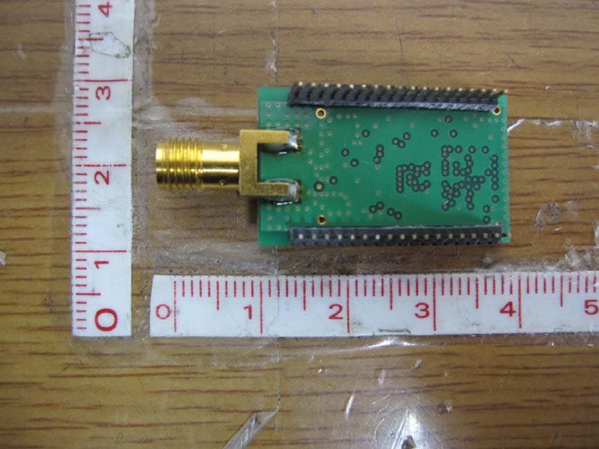
Click to zoom
Application Details
- Equipment Class
- DSS - Part 15 Spread Spectrum Transmitter
- Date of Grant
- May 10, 2012
- Application Purpose
- Original Equipment
- Date of Application
- May 10, 2012
- Equipment Note
- BLUETOOTH MODULE
- Frequency Range
- 2402.00000000 - 2480.00000000
- Company
- Sena Technologies Co., Ltd.
- Country
- South Korea
Documents & Files
Document Text
Text extracted from the exhibit documents filed with the FCC. Open a document above to read the original.
Users Manual
B B l l u u e e t t o o o o t t h h M M u u l l t t i i m m e e d d i i a a M M o o d d u u l l e e A A p p p p l l i i c c a a t t i i o o n n N N o o t t e e Sena Technologies, Inc. http://www.sena.com Page 1 of 24 Bluetooth ® Serial Module Application Note Bluetooth Class 2 OEM Module Model: Parani-BCD210 Ver 1.0 B B l l u u e e t t o o o o t t h h M M u u l l t t i i m m e e d d i i a a M M o o d d u u l l e e A A p p p p l l i i c c a a t t i i o o n n N N o o t t e e Sena Technologies, Inc. http://www.sena.com Page 2 of 24 1. General The Parani-BCD210 is a Bluetooth Class 2 OEM module for OEM manufacturers who want to implement Bluetooth Class 2 functionality with their products cost effectively and also in timely manner. Users can build their own antenna circuit around the BCD210 to lower the overall cost while benefit from the BCD210’s field-proven standard SPP (Serial Port Profile) firmware provided with no additional cost. The BCD210 supports Class 1 Bluetooth transmission level for longer communication distance typically ranges from 100 m up to 1 km. The BCD210 supports UART, USB, I2C, PCM, PIO interfaces for the communication with the OEM products. The BCD210 is provided with Bluetooth v2.0 compatible firmware runs internally for SPP (Serial Port Profile) applications by default. The SPP firmware supports up to 4 simultaneous multiple connections and is designed to work out-of-box for real world SPP applications such as POS (Point-of-sales), industrial automation, remote metering and other various applications. Optionally, the BCD210 can be supplied with only software stack up to HCI level so entire Bluetooth stack runs on the host side for the application such as USB dongles for computers, or OEM manufacturers can even develop and embed their own firmware into the BCD210. The BCD210 is fully qualified with Bluetooth v.2.0+EDR specification so OEM manufacturers can save cost and time for overall OEM product certifications, which makes the BCD210 ideal solution for larger volume and cost sensitive applications. To comply with FCC RF exposure compliance requirements, the antenna used for this transmitter must be installed to provide a separation distance of at least 20 cm from all persons and must not be co-located or operate in conjunction with any other antenna or transmitter.” As such, the radio component of this device is intended only for OEM integrators under the following two conditions: The antenna must be installed such that 20 cm is maintained between the antenna and users. The transmitter module may not be co-located with any other transmitter or antenna. As long as the two conditions above are met, further transmitter testing will not be required. However, the OEM integrator is still responsible for testing their end product for any additional compliance requirements required with this module installed (e.g., digital device emissions, PC peripheral requirements). In the event that these conditions cannot be met (for example, co-location with another transmitter), then the FCC authorization is no longer considered valid and the FCC ID cannot be used on the final product. In these circumstances, the OEM integrator will be responsible for re- evaluating the end product (including the transmitter) and obtaining a separate FCC B B l l u u e e t t o o o o t t h h M M u u l l t t i i m m e e d d i i a a M M o o d d u u l l e e A A p p p p l l i i c c a a t t i i o o n n N N o o t t e e Sena Technologies, Inc. http://www.sena.com Page 3 of 24 authorization. End Product Labeling The final end product must be labeled in a visible area with the following : “Contains Transmitter Module FCC ID: S7AIW03”. The radio component is an integral part of the Parani-BCD210DU and cannot be removed. 1.1 Features ■ Fully qualified Bluetooth v2.0 + EDR ■ Full-speed Bluetooth operation ■ Full piconet and scatternet support ■ Minimum external components ■ Low-power 1.8V operation ■ 1.8V core, 1.8 to 3.6V I/O ■ Integrated 1.8V regulator ■ 8 x 8mm, 96-ball TFBGA and 6 x 6mm, 96-ball, VFBGA package options ■ USB v2.0 and dual UART ports ■ Support for IEEE 802.11 coexistence ■ Support for 8Mbit external Flash ■ Green (RoHS and no antimony or halogenated flame retardants) 1.2 Applications ■ PCs ■ PDAs ■ Computer accessories (compact Flash cards, PCMCIA cards, SD cards and USB dongles) ■ Access points ■ Digital cameras B B l l u u e e t t o o o o t t h h M M u u l l t t i i m m e e d d i i a a M M o o d d u u l l e e A A p p p p l l i i c c a a t t i i o o n n N N o o t t e e Sena Technologies, Inc. http://www.sena.com Page 4 of 24 Model despription Model name Interface Connector Antenna Type1 Type2 Type3 Parani-BCD210DU DIP, pin U.FL 5dBi dipole 3dBi dipole 1dBi stub Parani-BCD210DS DIP, pin RPSMA 5dBi dipole 3dBi dipole 1dBi stub Parani-BCD210DC DIP, pin CHIP 0dBi Chip Parani-BCD210SU SMD, pad U.FL 5dBi dipole 3dBi dipole 1dBi stub Parani-BCD210SC SMD, pad CHIP 0dBi Chip Use Antenna Dipole antenna (M/N: R-AN2400-1901RS) Max Gain 5.37 dBi Dipole antenna (M/N: R-AN2400-5801RS) Max Gain 3.27 dBi Dipole antenna (M/N: AN2400-3306RS) Max Gain 1.40 dBi Chip antenna (SENA_F0615) Max Gain: 0.2dBi B B l l u u e e t t o o o o t t h h M M u u l l t t i i m m e e d d i i a a M M o o d d u u l l e e A A p p p p l l i i c c a a t t i i o o n n N N o o t t e e Sena Technologies, Inc. http://www.sena.com Page 5 of 24 1.3 Device Diagram 1.4 Pin Diagram B B l l u u e e t t o o o o t t h h M M u u l l t t i i m m e e d d i i a a M M o o d d u u l l e e A A p p p p l l i i c c a a t t i i o o n n N N o o t t e e Sena Technologies, Inc. http://www.sena.com Page 6 of 24 1.5 Pin Descriptions Function Pin Name Pin Number Description USB Interface USB_DP 8 USB data plus USB_DN 7 USB data minus UART Interface UART_TXD 11 UART data output UART_RXD 12 UART data input UART_RTS 10 UART request to send active low UART_CTS 9 UART clear to send active low PCM Interface PCM_OUT 25 Synchronous data output PCM_IN 24 Synchronous data …
Text truncated - open the document above for the full version.
Cover Letter(s)
Sena Technologies, Inc. 210 Yangjae-dong Seocho-gu Seoul 137-130 Korea Tel. +82-2-571-8283 Fax +82-2-573-7710 April 25, 2012 Federal Communications Commission Authorization and Evaluation Division 1435 Oakland Mills Road Columbia, MD 21046 In re : Sena Technologies, Inc. FCC Application for FCC ID: S7AIW03 To Whom It May Concern: We, the undersigned, hereby attest to the fact that we will apply the Declaration of Conformity procedure to the class B computer peripheral portion of this composite filing. Regards, YoungSam, KIM / Vice President Sena Technologies, Inc.
Cover Letter(s)
Sena Technologies, Inc. 210 Yangjae-dong Seocho-gu Seoul 137-130 Korea Tel. +82-2-571-8283 Fax +82-2-573-7710 April 25, 2012 Federal Communications Commission Equipment Authorization Branch 7435 Oakland Mills Road Columbia, MD 21046 LETTER OF AUTHORIZATION To whom it may concern: We, the undersigned, hereby authorize LTA Co., Ltd., to act on our behalf in all manners relating to application for equipment authorization for FCC ID: S7AIW03. including signing of all documents relating to these matters. Any and all acts carried out by LTA Co., Ltd., on our behalf shall have the same affect as acts of our own. This authorization is valid until further written notice from Sena Technologies, Inc. LTA Co.,LTD. (Contact Person) Contact name: LEE Kyu-Hyun Position: Manager Phone:(82)31-323-6008 E-mail: [email protected] YoungSam, KIM / Vice President Sena Technologies, Inc.
Cover Letter(s)
Sena Technologies, Inc. 210 Yangjae-dong Seocho-gu Seoul 137-130 Korea Tel. +82-2-571-8283 Fax +82-2-573-7710 April 25, 2012 Federal Communications Commission Equipment Authorization Branch 7435 Oakland Mills Road Columbia, MD 21046 In re : Sena Technologies, Inc. FCC ID : S7AIW03 Request for Confidentiality Pursuant to Sections 0.457 and 0.459 of the Commission’s Rules (CFR 47), and Section 552 (b) (4) of the Freedom of Information Act, Sena Technologies, Inc.. hereby requests confidentiality and treatment of certain information accompanying this application. The materials contain trade secrets and proprietary information not customarily released to the public. The public disclosure of these matters might be harmful to the Applicant and provide unjustified benefits to its competitors. We are also hereby request Short-Term Confidentiality for 180 days after the grant as outlined in Public Notice DA 04-1705. This provision will give Sena Technologies, Inc.. temporary confidentiality of commercially sensitive information prior to product release. The requested Confidential and Temporary Confidential exhibits are listed as follows: Exhibit Type File Name CONFIDENTIAL Schematics CONF APPENDIX S7AIW03 SCH DIA.pdf Parts list CONF APPENDIX S7AIW03 PL.pdf Block diagram CONF APPENDIX S7AIW03 BLK DIA.pdf Operational description CONF APPENDIX S7AIW03 OpDes.pdf SHORT-TERM CONFIDENTIAL External Photos SHORT-TERM CONF S7AIW03 EXT Photo.pdf Internal Photos SHORT-TERM CONF S7AIW03 INT Photo.pdf Test-Setup Photos SHORT-TERM CONF S7AIW03 Test Photo.pdf User’s Manual SHORT-TERM CONF S7AIW03 Manual.pdf The Applicant understands that pursuant to Rule 0.457, disclosure of this application and all accompanying documentations, where applicable, will not be made public before the date of the Grant for this application. YoungSam, KIM / Vice President Sena Technologies, Inc.
Cover Letter(s)
Sena Technologies, Inc. 210 Yangjae-dong Seocho-gu Seoul 137-130 Korea Tel. +82-2-571-8283 Fax +82-2-573-7710 ATTESTATION STATEMENT In re : SENA Technologies, Inc. FCC ID: S7AIW03 Date : April 25, 2012 15.247(a)(1) The hopping sequence must be pseudorandom all Channels are used equally on average the receiv er input bandwidth is approximately equal to the transmit bandwidth the receiver hops in sequence with the transmitted signal 15.247(g) The system is designed to comply with all of the regulations in Section 15.247 when the transmitter is presented with a continuous data (or information) 15.247(h) The system does not coordinate its channel selection/hopping sequence with other frequency hopping systems for the express purpose of avoiding the simultaneous occupancy of individual hopping frequ encies by multiple transmitters. Sincerely, YoungSam, KIM / Vice President Sena Technologies, Inc.
Cover Letter(s)
Sena Technologies, Inc. 210 Yangjae-dong Seocho-gu Seoul 137-130 Korea Tel. +82-2-571-8283 Fax +82-2-573-7710 FCC ID: S7AIW03 Request for transmitter Modular approval Transmitter Module Characteristics No Requirements EUT 1 Have its own RF shielding Device is equipped with metal shielding to cover RF section. Refer to external photos. 2 Have buffered modulation/data inputs (if such inputs are provided) All inputs to the modules are buffered th ought logic or microprocessor inputs. 3 Have it own power supply regulation Internal 1.8V power regulation. Refer to Module Block diagram 4 Meet the antenna requirements of Section 15.203 BCD210DU, BCD210SU is equipped with unique antenna connector (U.FL) BCD210DS is equipped with unique antenna connector (RPSMA). BCD210DC, BCD210SC is equipped with SMD antenna (Chip). Refer to external photos. 5 Be tested in a stand-alone configuration, i.e., the antenna, AC or DC power and data input/output lines must be connected to the module but, the module must not be inside another case during testing Device was tested on a supplied development platform for Single modular approval. Refer to setup photos. 6 Be labeled with its own FCC ID number, and if the FCC ID is not visible when the module is installed inside another device, then the out side of the device into which the module is installed must also display a label referring to the enclosed module Label is to be placed in front of the EUT (P arani-BCD210DU), and other label is to be placed in the User’s Guide. Refer to FCC ID label format. 7 The modular transmitter is manufactured so t hat the user cannot influence the operation of the transmitter that will operate outsi de of the scope of the regulations. Refer to “User’s Guide” 8 Address compliance with the Commission’s RF exposure limits in Sections 1.1310 and 2.1091. In addition, spread spectrum transmitters operating under Section 15.247 are required to address RF exposure compliance in accordance with Section 15.247(b)(4). This device is categorically from routine environmental because it operate at very low power level
External Photos
FCC ID: S7AIW03 IC : 8154A-IW03 Copyright ○ c 2012, LTA Co., Ltd. Page 1 of 14 Parani-BCD210DU Basic model (DIP Type & U.FL Type) Upper Lower FCC ID: S7AIW03 IC : 8154A-IW03 Copyright ○ c 2012, LTA Co., Ltd. Page 2 of 14 Front Rear FCC ID: S7AIW03 IC : 8154A-IW03 Copyright ○ c 2012, LTA Co., Ltd. Page 3 of 14 Parani-BCD210DS ADD Model (DIP Type & RP-SMA Type) Upper Lower FCC ID: S7AIW03 IC : 8154A-IW03 Copyright ○ c 2012, LTA Co., Ltd. Page 4 of 14 Front Rear FCC ID: S7AIW03 IC : 8154A-IW03 Copyright ○ c 2012, LTA Co., Ltd. Page 5 of 14 Parani-BCD210DC Add Model(DIP Type & Chip Type) Upper Lower FCC ID: S7AIW03 IC : 8154A-IW03 Copyright ○ c 2012, LTA Co., Ltd. Page 6 of 14 Front Rear FCC ID: S7AIW03 IC : 8154A-IW03 Copyright ○ c 2012, LTA Co., Ltd. Page 7 of 14 Parani-BCD210SU ADD Model(SMD Type & U.FL Type) Upper Lower FCC ID: S7AIW03 IC : 8154A-IW03 Copyright ○ c 2012, LTA Co., Ltd. Page 8 of 14 Front Rear FCC ID: S7AIW03 IC : 8154A-IW03 Copyright ○ c 2012, LTA Co., Ltd. Page 9 of 14 Parani-BCD210SC ADD Model(SMD Type & Chip Type) Upper Lower FCC ID: S7AIW03 IC : 8154A-IW03 Copyright ○ c 2012, LTA Co., Ltd. Page 10 of 14 Front Rear FCC ID: S7AIW03 IC : 8154A-IW03 Copyright ○ c 2012, LTA Co., Ltd. Page 11 of 14 ANTENNA- M/N: R-AN2400-1901RS FCC ID: S7AIW03 IC : 8154A-IW03 Copyright ○ c 2012, LTA Co., Ltd. Page 12 of 14 ANTENNA- M/N: R-AN2400-5801RS FCC ID: S7AIW03 IC : 8154A-IW03 Copyright ○ c 2012, LTA Co., Ltd. Page 13 of 14 ANTENNA- M/N: AN2400-3306RS FCC ID: S7AIW03 IC : 8154A-IW03 Copyright ○ c 2012, LTA Co., Ltd. Page 14 of 14 ANTENNA- M/N: SENA_F0160
ID Label/Location Info
FCC ID: S7AIW03 IC : 8154A-IW03 Copyright Ⓒ 2012, LTA Co., Ltd. SAMPLE LABEL & LOCATION M/N Interface Type ANT Connector TypeType Description BCD210DU DIP Type U.FL DDIP(Interface) BCD210DC DIP Type CHIP SSMD(Interface) BCD210DS DIP Type RPSMA U U.FL Connector ANT BCD210SC SMD Type CHIP CCHIP ANT BCD210SU SMD Type U.FL S RPSMA Connector ANT
Internal Photos
FCC ID: S7AIW03 IC: 8154A-IW03 Copyright ○ c 2012, LTA Co., Ltd. Page 1 of 1 MainBoard - Front MainBoard - Rear
RF Exposure Info
FCC ID: S7AIW03 ATTACHMENT ** MPE Calculations ** The MPE calculation for this exposure is shown below. The peak radiated output power (EIRP) is calculated as follows: EIRP = P + G EIRP = 4.81 dBm + 5.37 dBi EIRP = 10.18 dBm Where, P = Power input to the antenna (mW) G = Powe rgain of the antenna (dBi) Power density at the specific separation: S = PG/(4R 2 π) Where, S = Maximum power density (mW/cm 2 ) P = Power input to the antenna (mW) G = Numeric power gain of the antenna R = Distance to the center of the radiation of the antenna (20cm = limit for MPE) S = (3.03 *3.44) / (4 * 20 2 * π) S = 0.0021 mW/cm 2 The Maximum permissible exposure (MPE) for the general population is 1 mW/cm 2 . The power density does not exceed the 1 mW/cm 2 limit. Therefore, the exposure condition is compliant with FCC rules. Estimated safe separation: R = √(PG / 4π) Where, P = Power input to the antenna (mW) G = Numeric power gain of the antenna R = Distance to the center of the radiation of the antenna (20cm = limit for MPE) R = √(3.03*3.44 / 4π) R = 0.91 Cm The numeric gain(G) of the antenna with a gain specified in dB is determined by: G = Log -1 (dB antenna gain / 10) G = Log -1 (5.37 / 10) G = 3.44
Test Report
Ref. No.: LR500111204I Copyright ○ c 2012, LTA Co., Ltd. Page 1 of 53 243 Jubug-Ri,Yangji-Myeon, Yongin-Si, Gyeonggi-Do, Korea 449-822 Tel: +82-31-323-6008 Fax: +82-31-323-6010 http://www.ltalab.com Dates of Tests: April 19 ~26, 2012 Test Report S/N: LR500111204I Test Site : LTA CO., LTD. CERTIFICATION OF COMPLIANCE FCC ID IC APPLICANT Equipment Class : Part 15 Spread Spectrum Transmitter (DSS) Manufacturing Description : Bluetooth Module Manufacturer : Sena Technologies, Inc. Model name : Parani-BCD210DU Variant Model name : Parani-BCD210DS, Parani-BCD210DC Parani-BCD210SU, Parani-BCD210SC Test Device Serial No.: : Identical prototype Rule Part(s) : FCC Part 15.247 Subpart C; ANSI C-63.4-2003 RSS-210 and ISSUE No. :8 Date :2010 Frequency Range : 2402 ~ 2480MHz RF power : Max 4.81 dBm - Conducted Data of issue : April 30, 2012 This test report is issued under the authority of: The test was supervised by: Kyu-Hyun Lee, Manager Ki-Hun Cho, Test Engineer This test result only responds to the tested sample. It is not allowed to copy this report even partly without the allowance of the test laboratory. The report must not be used by the client to claim product certification, approval, or endorsement by NVLAP, NIST, or any agency of the Federal Government. NVLAP LAB Code.: 200723-0 S7AIW03 8154A-IW03 Sena Technologies, Inc. Ref. No.: LR500111204I Copyright ○ c 2012, LTA Co., Ltd. Page 2 of 53 TABLE OF CONTENTS 1. GENERAL INFORMATION’S -------------------------------------------------------------------------- 2. INFORMATION’S ABOUT TEST ITEM ------------------------------------------------------------- 3. TEST REPORT --------------------------------------------------------------------------------------------- 3.1 SUMMARY OF TESTS ------------------------------------------------------------------------------ 3.2 TECHNICAL CHARACTERISTICS TEST ------------------------------------------------------- 3.2.1 CARRIER FREQUENCY SEPARATION ---------------------------------------------------- 3.2.2 NUMBER OF HOPPING FREQUENCIES -------------------------------------------------- 3.2.3 20 dB BANDWIDTH ---------------------------------------------------------------------------- 3.2.4 TIME OF OCCUPANCY (Dwell Time) ------------------------------------------------------- 3.2.5 TRANSMITTER OUTPUT POWER ---------------------------------------------------------- 3.2.6 BAND – EDGE & SPURIOUS ----------------------------------------------------------------- 3.2.7 FIELD STRENGTH OF HARMONICS-Transmitter ------------------------------------------- 3.2.8 FIELD STRENGTH OF HARMONICS-Receiver ---------------------------------------------- 3.2.9 AC CONDUCTED EMISSIONS -------------------------------------------------------------- APPENDIX APPENDIX TEST EQUIPMENT USED FOR TESTS -------------------------------------------- 3 4 5 5 6 6 8 10 17 23 27 34 42 51 52 Ref. No.: LR500111204I Copyright ○ c 2012, LTA Co., Ltd. Page 3 of 53 1. General information’s 1-1 Test Performed Company name : LTA Co., Ltd. Address : 243, Jubug-ri,Yangji-Myeon,Youngin-Si, Kyunggi-Do, Korea. 449-822 Web site : http://www.ltalab.com E-mail : [email protected] Telephone : +82-31-323-6008 Facsimile +82-31-323-6010 Quality control in the testing laboratory is implemented as per ISO/IEC 17025 which is the “General requirements for the competents of calibration and testing laboratory”. 1-2 Accredited agencies LTA Co., Ltd. is approved to perform EMC testing by the following agencies: Agency Country Accreditation No. Validity Reference NVLAP U.S.A 200723-0 2012-09-30 ECT accredited Lab. RRL KOREA KR0049 2013-04-24 EMC accredited Lab. FCC U.S.A 610755 2014-04-27 FCC filing FCC U.S.A 649054 2013-04-13 FCC CAB VCCI JAPAN R2133(10m), C2307 2014-06-21 VCCI registration VCCI JAPAN T-2009 2013-12-23 VCCI registration IC CANADA IC5799 2012-05-14 IC filing Ref. No.: LR500111204I Copyright ○ c 2012, LTA Co., Ltd. Page 4 of 53 2. Information’s about test item 2-1 Client & Manufacturer Company name : Sena Technologies, Inc. Address : 210 Yangjae-dong Seocho-gu Seoul 137-130 Korea Telephone / Facsimile : +82-2-571-8283/ +82-2-573-7710 2-2 Equipment Under Test (EUT) Trade name : Bluetooth Module FCC ID : S7AIW03 Model name : Parani-BCD210DU Serial number : Identical prototype Date of receipt : April 17, 2012 EUT condition : Pre-production, not damaged Antenna type : Dipole antenna (M/N: R-AN2400-1901RS) Max Gain 5.37 dBi Dipole antenna (M/N: R-AN2400-5801RS) Max Gain 3.27 dBi Dipole antenna (M/N: AN2400-3306RS) Max Gain 1.40 dBi Chip antenna (SENA_F0615) Max Gain: 0.2dBi Frequency Range : 2402 ~ 2480MHz RF output power : Max.4.81 dBm - Conducted Number of channels : 79 Duty cycle : 80.90 % Channel spacing : 1MHz Channel Access Protocol : Frequency Hopping Spread Spectrum (FHSS) Type of Modulation : Basic Mode(GFSK), EDR Mode(Pi/4 DQPSK, 8DPSK) Power Source : 3.3Vdc by Main System Firmware Version : V1.0.0 2-4 Tested frequency LOW MID HIGH Frequency (MHz) 2402 2441 2480 Ref. No.: LR500111204I Copyright ○ c 2012, LTA Co., Ltd. Page 5 of 53 2-5 Ancillary Equipment Equipment Model No. Serial No. Manufacturer Notebook PP37L 29705283757 DELL MOUSE SMH-210U M2UWTAKQ605877M MONTEREY INTERNATIONAL CORP PRINTER Deskjet 600K SG763131XX HP DC Power Supply E3615A KR72705061 HP 2-6 Model Description M/N Interface Type ANT Connector Type Type Description Parani-BCD210DU DIP Type U.FL D DIP(Interface) Parani-BCD210DC DIP Type CHIP S SMD(Interface) Parani-BCD210DS DIP Type RPSMA U U.FL Connector ANT Parani-BCD210SC SMD Type CHIP C CHIP ANT Parani-BCD210SU SMD Type U.FL S RPSMA Connector ANT Ref. No.: LR500111204I Copyright ○ c 2012, LTA Co., Ltd. Page 6 of 53 3. Test Report 3.1 Summary of tests FCC Part Section(s) Parameter Limit Test Condition Status (note 1) 15.247(a) Carrier Frequency Separation > 25 kHz Conducted C 15.247(a) Number of Hopping Frequencies > 15 hops C 15.247(a) 20 dB Bandwidth 99% Bandwidth > 1.5 MHz C 15.247 Dwell Time < 0.4 seconds C 15.247(b) Transmitter Output P…
Text truncated - open the document above for the full version.
Test Setup Photos
FCC ID: S7AIW03 IC: 8154A-IW03 Copyright ○ c 2012, LTA Co., Ltd. Page 1 of 2 Radiated Emission FCC ID: S7AIW03 IC: 8154A-IW03 Copyright ○ c 2012, LTA Co., Ltd. Page 2 of 2 Radiated Emission
Contact Information
Applicant
Seunghyun KIM(Research Engineer)
Test Firm
LTA Co.,LtdAhn Chulho
Technical Specifications
| # | Rule Parts | Frequency Range | Power Output |
|---|---|---|---|
| 1 | 15C | 2.40 GHz - 2.48 GHz | 3.00 mW |
Other Applications from Sena Technologies Co., Ltd.
S7A-SP196
Jun 15, 2026Wireless Communication Systems
Equipment Class
NII - Unlicensed National Information Infrastructure TXS7A-SP198
May 07, 2026Wireless Communication Systems
Equipment Class
DTS - Digital Transmission SystemS7A-SP197
Apr 06, 2026Wireless Communication Systems
Equipment Class
DTS - Digital Transmission SystemS7A-SP195
Apr 06, 2026Wireless Communication Systems
Equipment Class
DTS - Digital Transmission SystemS7A-SP158
Mar 13, 2026Wireless Communication Systems
Equipment Class
DSS - Part 15 Spread Spectrum Transmitter