S7AZBLINXZE10ZIGBEE SERIAL MODULE
Sena Technologies Co., Ltd.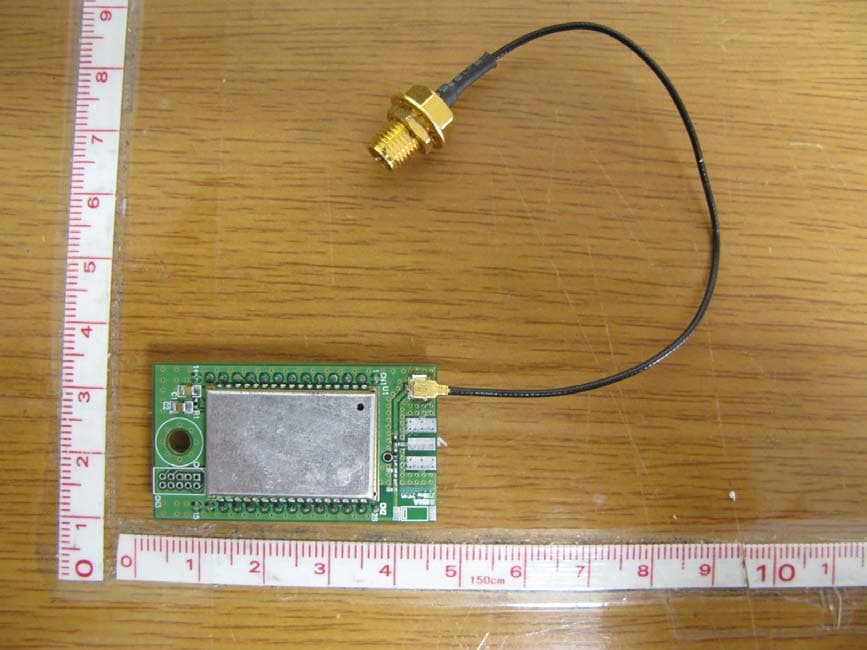
Click to zoom
Application Details
- Equipment Class
- DTS - Digital Transmission System
- Date of Grant
- Feb 07, 2010
- Application Purpose
- Original Equipment
- Date of Application
- Feb 04, 2010
- Equipment Note
- ZIGBEE SERIAL MODULE
- Frequency Range
- 2410.00000000 - 2475.00000000
- Company
- Sena Technologies Co., Ltd.
- Country
- South Korea
Documents & Files
Document Text
Text extracted from the exhibit documents filed with the FCC. Open a document above to read the original.
Users Manual
ZBlinx-Z series User Guide Version 0.0.1 2010-02-04 User Guide for the ZBlinx-Z series Version 0.0.1 Firmware version 1.0.X Last revised on January 12, 2010 Printed in Korea Copyright Copyright 2002, SENA technologies, Inc. All rights reserved. SENA Technologies reserves the right to make changes and improvements to its product without providing notice. Trademark ZBlinx™ is a trademark of SENA Technologies, Inc. Windows® is a registered trademark of Microsoft Corporation. Ethernet® is a registered trademark of XEROX Corporation. Notice to Users When a system failure may cause serious consequences, protecting life and property against such consequences with a backup system or safety device is essential. The user agrees that protection against consequences resulting from system failure is the user's responsibility. This device is not approved for life-support or medical systems. Changes or modifications to this device not explicitly approved by SENA Technologies will void the user's authority to operate this device. Precautions and Safety Electricity Use only the supplied AC adapter. Use of unauthorized power adapter is not recommended. Electrical shock may result. Do not kink or crease the power cable or place heavy objects on the power cable. Fire can result from damaged power cables. Do not handle power plug and adapter with wet hands. Electrical shock may result. Immediately power off the product and unplug the AC adapter if smoke or odors emit from the product and adapter. Fire can result from improper use. Immediately power off the product and unplug the AC adapter if water or other liquids are present. Fire can result from improper use. Product ZBlinx-Z meets the RS-232 standards. Do not wire with non-standard products. Damage to your products may result from improper use. Do not drop or subject the device to impact. Damage to your products may result from improper use. Keep away from harsh environments including humid, dusty, and smoky areas. Damage to your products may result from improper use. Do not use excessive force on the buttons or attempt to disassemble the device. Damage to your products may result from improper use. Do not place heavy objects on the product. Damage to your products may result from improper use. Technical Support SENA Technologies, Inc. 210 Yangjae-dong, Seocho-gu Seoul 137-130, Korea Tel: (+82-2) 573-5422 Fax: (+82-2) 573-7710 E-Mail: [email protected] Website: http://www.sena.com Revision History Revision Date Name Description V0.0.1 2010-01-12 Initial Revision History - 4 - Contents 1. Introduction ...................................................................................................................................... 6 1.1. Overview........................................................................................................................... 6 1.2. Product Specification ........................................................................................................ 7 2. Approval Information........................................................................................................................ 8 2.1. FCC .................................................................................................................................. 8 2.1.1. FCC Compliance Statement ..................................................................................... 8 2.1.2. RF Exposure Statement............................................................................................ 8 2.1.3. Do not ....................................................................................................................... 8 2.2. CE..................................................................................................................................... 8 2.2.1. EC-R&TTE Directive................................................................................................. 8 2.3. TELEC .............................................................................................................................. 8 2.4. KCC .................................................................................................................................. 8 3. RF Information ................................................................................................................................. 9 3.1. Radio Frequency Range .................................................................................................. 9 3.2. Number of Frequency Channel ........................................................................................ 9 3.3. Transmission Method .......................................................................................................9 3.4. Modulation Method ........................................................................................................... 9 3.5. Radio Output Power .........................................................................................................9 3.6. Receiving Sensitivity ........................................................................................................ 9 4. AT Command ................................................................................................................................. 10 4.1. Overview......................................................................................................................... 10 4.2. Command Line Format................................................................................................... 10 4.3. Standard AT Commands..................................................................................................11 4.3.1. AT.............................................................................................................................11 4.3.2. ATA...........................................................................................................................11 4.3.3. ATD<node ID or IEEE address>..................…
Text truncated - open the document above for the full version.
Cover Letter(s)
Sena Technologies, Inc. 210 Yangjae-dong Seocho-gu Seoul 137-130 Korea Tel. +82-2-571-8283 Fax +82-2-573-7710 January 29, 2010 Federal Communications Commission Equipment Authorization Branch 7435 Oakland Mills Road Columbia, MD 21046 LETTER OF AUTHORIZATION To whom it may concern: We, the undersigned, hereby authorize LTA Co., Ltd., to act on our behalf in all manners relating to application for equipment authorization for FCC ID: S7AZBLINXZE10. including signing of all documents relating to these matters. Any and all acts carried out by LTA Co., Ltd., on our behalf shall have the same affect as acts of our own. This authorization is valid until further written notice from Sena Technologies, Inc. LTA Co.,LTD. (Contact Person) Contact name: LEE, Kyung-Taek Position: Manager Phone:(82)31-323-6008 E-mail: [email protected] YoungSam, KIM / Vice President Sena Technologies, Inc.
Cover Letter(s)
Sena Technologies, Inc. 210 Yangjae-dong Seocho-gu Seoul 137-130 Korea Tel. +82-2-571-8283 Fax +82-2-573-7710 January 29, 2010 Federal Communications Commission Equipment Authorization Branch 7435 Oakland Mills Road Columbia, MD 21046 In re : Sena Technologies, Inc. FCC ID : S7AZBLINXZE10 Request for Confidentiality Pursuant to Sections 0.457 and 0.459 of the Commission’s Rules (CFR 47), and Section 552 (b) (4) of the Freedom of Information Act, Sena Technologies, Inc.. hereby requests confidentiality and treatment of certain information accompanying this application. The materials contain trade secrets and proprietary information not customarily released to the public. The public disclosure of these matters might be harmful to the Applicant and provide unjustified benefits to its competitors. We are also hereby request Short-Term Confidentiality for 180 days after the grant as outlined in Public Notice DA 04-1705. This provision will give Sena Technologies, Inc.. temporary confidentiality of commercially sensitive information prior to product release. The requested Confidential and Temporary Confidential exhibits are listed as follows: Exhibit Type File Name Schematics CONF APPENDIX S7AZBLINXZE10 SCH DIA.pdf Parts list CONF APPENDIX S7AZBLINXZE10 PL.pdf Block diagram CONF APPENDIX S7AZBLINXZE10 BLK DIA.pdf CONFIDENTIAL Operational description CONF APPENDIX S7AZBLINXZE10 OpDes.pdf External Photos SHORT-TERM CONF S7AZBLINXZE10 EXT Photo.pdf Internal Photos SHORT-TERM CONF S7AZBLINXZE10 INT Photo.pdf Test-Setup Photos SHORT-TERM CONF S7AZBLINXZE10 Test Photo.pdf SHORT-TERM CONFIDENTIAL User’s Manual SHORT-TERM CONF S7AZBLINXZE10 Manual.pdf The Applicant understands that pursuant to Rule 0.457, disclosure of this application and all accompanying documentations, where applicable, will not be made public before the date of the Grant for this application. YoungSam, KIM / Vice President Sena Technologies, Inc.
Cover Letter(s)
Sena Technologies, Inc. 210 Yangjae-dong Seocho-gu Seoul 137-130 Korea Tel. +82-2-571-8283Fax +82-2-573-7710 FCC ID: S7AZBLINXZE10 Request for Limited Modular approval Transmitter Module Characteristics The module will be used to the manufac tured product by Sena Technologies, Inc . No Requirements EUT 1 Have its own RF shielding Device is equipped with metal shielding to cover RF section. Refer to external photos. 2 Have buffered modulation/data inputs (if such inputs are provided) All inputs to the modules are buffered th ought logic or microprocessor inputs. 3 Have it own power supply regulation Internal 3.3V powe r regulation. Refer to Module Block diagram and schematic 4 Meet the antenna requirements of Section 15.203 Refer to internal photos. The antenna connector is the reverse polar ity SMA connector. And Chip,Whip antenna 5 Be tested in a stand-alone configuration, i.e., the antenna, AC or DC power and data input/output lines must be connected to the module but, the module must not be inside another case during testing Device was tested on a supplied development platform for limited modular approval. Refer to setup photos. 6 Be labeled with its own FCC ID number, and if the FCC ID is not visible when the module is installed inside another device, then the out side of the device into which the module is installed must also display a label referring to the enclosed module Label is to be placed in front of the EUT(ZBlinx- ZE10 ), and other label is to be placed in the User’s Guide. Refer to FCC ID label format. 7 The modular transmitter is manufactured so t hat the user cannot influence the operation of the transmitter that will operate outsi de of the scope of the regulations. Refer to “User’s Guide” 8 Address compliance with the Commission’s RF exposure limits in Sections 1.1310 and 2.1091. In addition, spread spectrum transmitters operating under Section 15.247 are required to address RF exposure compliance in accordance with Section 15.247(b)(4). This device is categorically excluded from routine environmental because it operate at very low power level
External Photos
FCC ID: S7AZBLINXZE10 Copyright ○ c 2010, LTA Co., Ltd. Page 1 of 8 Basic model Upper Lower 23mm 52mm FCC ID: S7AZBLINXZE10 Copyright ○ c 2010, LTA Co., Ltd. Page 2 of 8 Coaxial type Upper Lower 23mm 46mm FCC ID: S7AZBLINXZE10 Copyright ○ c 2010, LTA Co., Ltd. Page 3 of 8 Chip type Upper Lower 23mm 46mm FCC ID: S7AZBLINXZE10 Copyright ○ c 2010, LTA Co., Ltd. Page 4 of 8 Whip type Upper Lower 23mm 46mm FCC ID: S7AZBLINXZE10 Copyright ○ c 2010, LTA Co., Ltd. Page 5 of 8 ANTENNA- M/N: R-AN2400-1901RS FCC ID: S7AZBLINXZE10 Copyright ○ c 2010, LTA Co., Ltd. Page 6 of 8 ANTENNA- M/N: R-AN2400-5801RS FCC ID: S7AZBLINXZE10 Copyright ○ c 2010, LTA Co., Ltd. Page 7 of 8 ANTENNA- M/N: AN2400-3306RS FCC ID: S7AZBLINXZE10 Copyright ○ c 2010, LTA Co., Ltd. Page 8 of 8 ANTENNA- M/N: SENA_029 ANTENNA- M/N: SENA_W01
ID Label/Location Info
FCC ID: S7AZBLINXZE10 Copyright Ⓒ 2010, LTA Co., Ltd. SAMPLE LABEL & LOCATION S U W C S: RP-SMA Connector U: U.FL Connector W: Whip Ant C: Chip Ant Note : Antenna connecting type check
Internal Photos
FCC ID: S7AZBLINXZE10 Copyright ○ c 2010, LTA Co., Ltd. Page 1 of 1 MainBoard - Front MainBoard - Rear
RF Exposure Info
FCC ID: S7AZBLINXZE10 ATTACHMENT ** MPE Calculations ** The MPE calculation for this exposure is shown below. The peak radiated output power (EIRP) is calculated as follows: EIRP = P + G EIRP = 13.10dBm + 5.37dBi EIRP = 18.47 dBm Where, P = Power input to the antenna (mW) G = Power gain of the antenna (dBi) Power density at the specific separation: S = PG/(4R 2 π) S = (20.42 * 3.44) / (4 * 20 2 * π) S = 0.0140 mW/cm 2 Where, S = Maximum power density (mW/cm 2 ) P = Power input to the antenna (mW) G = Numeric power gain of the antenna R = Distance to the center of the radiation of the antenna (20cm = limit for MPE) The Maximum permissible exposure (MPE) for the general population is 1 mW/cm 2 . The power density does not exceed the 1 mW/cm 2 limit. Therefore, the exposure condition is compliant with FCC rules. Estimated safe separation: R = √(PG / 4π) R = √(20.42* 3.44 / 4π) R = 2.37Cm Where, P = Power input to the antenna (mW) G = Numeric power gain of the antenna R = Distance to the center of the radiation of the antenna (20cm = limit for MPE) The numeric gain(G) of the antenna with a gain specified in dB is determined by: G = Log -1 (dB antenna gain / 10) G = Log -1 (0 / 10) G = 3.44
Test Report
Ref. No.: LR5001901002A Copyright ○ c 2010, LTA Co., Ltd. Page 1 of 31 243 Jubug-Ri,Yangji-Myeon, Yongin-Si, Gyeonggi-Do, Korea 449-822 Tel: +82-31-323-6008 Fax: +82-31-323-6010 http://www.ltalab.com Dates of Tests: Jan 20 ~ 29, 2010 Test Report S/N: LR500191002A Test Site : LTA CO., LTD. CERTIFICATION OF COMPLIANCE FCC ID. APPLICANT Equipment Class : Digital Transmission System (DTS) Manufacturing Description : ZigBee Serial Module Manufacturer : Sena Technologies, Inc. Model name : ZBlinx-ZE10 Test Device Serial No.: : Identical prototype Rule Part(s) : FCC Part 15.247 Subpart C; ANSI C-63.4-2003 Frequency Range : 2410MHz ~ 2475MHz Max. Output Power : Max 13.10dBm - Conducted Data of issue : February 1, 2010 This test report is issued under the authority of: The test was supervised by: Dong –Min JUNG, Technical Manager Kyung-Taek LEE, Test Engineer This test result only responds to the tested sample. It is not allowed to copy this report even partly without the allowance of the test laboratory. This report must not be used by the applicant to claim product endorsement by any agency. NVLAP LAB Code.: 200723-0 S7AZBLINXZE10 Sena Technologies, Inc. Ref. No.: LR5001901002A Copyright ○ c 2010, LTA Co., Ltd. Page 2 of 31 TABLE OF CONTENTS 1. GENERAL INFORMATION’S -------------------------------------------------------------------------- 2. INFORMATION’S ABOUT TEST ITEM ------------------------------------------------------------- 3. TEST REPORT --------------------------------------------------------------------------------------------- 3.1 SUMMARY OF TESTS ------------------------------------------------------------------------------ 3.2 TECHNICAL CHARACTERISTICS TEST ------------------------------------------------------- 3.2.1 6dB BANDWIDTH ------------------------------------------------------------------------------ 3.2.2 PEAK OUTPUT POWER ----------------------------------------------------------------------- 3.2.3 POWER SPECTRAL DENSITY --------------------------------------------------------------- 3.2.4 BAND – EDGE & SPURIOUS ----------------------------------------------------------------- 3.2.5 FIELD STRENGTH OF HARMONICS ------------------------------------------------------ 3.2.6 AC CONDUCTED EMISSIONS -------------------------------------------------------------- APPENDIX APPENDIX TEST EQUIPMENT USED FOR TESTS -------------------------------------------- 3 4 5 5 6 6 9 12 15 21 27 30 Ref. No.: LR5001901002A Copyright ○ c 2010, LTA Co., Ltd. Page 3 of 31 1. General information’s 1-1 Test Performed Company name : LTA Co., Ltd. Address : 243, Jubug-ri,Yangji-Myeon,Youngin-Si, Kyunggi-Do, Korea. 449-822 Web site : http://www.ltalab.com E-mail : [email protected] Telephone : +82-31-323-6008 Facsimile +82-31-323-6010 Quality control in the testing laboratory is implemented as per ISO/IEC 17025 which is the “General requirements for the competents of calibration and testing laboratory”. 1-2 Accredited agencies LTA Co., Ltd. is approved to perform EMC testing by the following agencies: Agency Country Accreditation No. Validity Reference NVLAP U.S.A 200723-0 2010-09-30 ECT accredited Lab. RRL KOREA KR0049 2011-06-20 EMC accredited Lab. FCC U.S.A 610755 2011-04-22 FCC filing VCCI JAPAN R2133, C2307 2011-06-21 VCCI registration IC CANADA IC5799 2010-05-03 IC filing Ref. No.: LR5001901002A Copyright ○ c 2010, LTA Co., Ltd. Page 4 of 31 2. Information’s about test item 2-1 Client & Manufacturer Company name : Sena Technologies, Inc. Address : 210 Yangjae-dong Seocho-gu Seoul 137-130 Korea Tel / Fax : +82-2-571-8283/ +82-2-573-7710 2-2 Equipment Under Test (EUT) Trade name : ZigBee Serial Module FCC ID : S7AZBLINXZE10 Model name : ZBlinx-ZE10 Serial number : Identical prototype Date of receipt : January 20, 2010 EUT condition : Pre-production, not damaged Antenna type : Dipole antenna (M/N: R-AN2400-1901RS) Max Gain 5.37 dBi Dipole antenna (M/N: R-AN2400-5801RS) Max Gain 3.27 dBi Dipole antenna (M/N: AN2400-3306RS) Max Gain 1.40 dBi Chip antenna (SENA_029) Max Gain: 0.5dBi Whip antenna (SENA_W01) Max Gain: 2.1dBi Frequency Range : 2410MHz ~ 2475MHz (DSSS) RF output power : Max 13.10dBm - Conducted Number of channels : 14 Type of Modulation : O-QPSK Channel spacing : 5MHz Power Source : 3.3Vdc by Main System 2-3 Tested frequency LOW MID HIGH Frequency (MHz) 2410 2445 2475 2-4 Ancillary Equipment Equipment Model No. Serial No. Manufacturer PC HP Compaq dx7400 Microtower CNG8330J95 HP MONITOR HPL1710 CNC816QHF2 HP KEYBOARD SK-8115 68A-04Q6 DELL MOUSE MO56UO 520107013 DELL PRINTER STYLUS C65 N/A EPSON Ref. No.: LR5001901002A Copyright ○ c 2010, LTA Co., Ltd. Page 5 of 31 3. Test Report 3.1 Summary of tests FCC Part Section(s) Parameter Limit Test Conditio n Status (note 1) 15.247(a) 6 dB Bandwidth > 500kHz C 15.247(b) Transmitter Peak Output Power < 1Watt C 15.247(d) Transmitter Power Spectral Density < 8dBm @ 3kHz C 15.247(d) Band Edge & Spurious > 20 dBc Conducted C 15.209 Field Strength of Harmonics Emission Radiated C 15.207 AC Conducted Emissions Emissions Conducted C 15.203 Antenna requirement - - C Note 1: C=Complies NC=Not Complies NT=Not Tested NA=Not Applicable Note 2: The data in this test report are traceable to the national or international standards. Antenna Requirement The Sena Technologies, Inc. FCC ID: S7AZBLINXZE10 unit complies with the requirement of §15.203. The antenna connector is the reverse polarity SMA connector. And Chip antenna The Whip antenna is the Molding Type The sample was tested according to the following specification: FCC Parts 15.247; ANSI C-63.4-2003 Ref. No.: LR5001901002A Copyright ○ c 2010, LTA Co., Ltd. Page 6 of 31 3.2 Technical Characteristics Test 3.2.1 6 dB Bandwidth Procedure: The bandwidth at 6dB below the highest in-band spectral density was measured with a spectrum analyzer connected to the antenna terminal, while EUT is operating in transmission mode at the appropriate frequencies. After the trace being stable, Use the marker-to-peak function t…
Text truncated - open the document above for the full version.
Test Setup Photos
FCC ID: S7AZBLINXZE10 Copyright ○ c 2010, LTA Co., Ltd. Page 1 of 2 Radiated Emission FCC ID: S7AZBLINXZE10 Copyright ○ c 2010, LTA Co., Ltd. Page 2 of 2 Conducted Emission
Contact Information
Applicant
Seunghyun KIM(Research Engineer)
Test Firm
LTA Co.,LtdAhn Chulho
Technical Specifications
| # | Rule Parts | Frequency Range | Power Output |
|---|---|---|---|
| 1 | 15C | 2.41 GHz - 2.48 GHz | 20.00 mW |
Other Applications from Sena Technologies Co., Ltd.
S7A-SP196
Jun 15, 2026Wireless Communication Systems
Equipment Class
NII - Unlicensed National Information Infrastructure TXS7A-SP198
May 07, 2026Wireless Communication Systems
Equipment Class
DTS - Digital Transmission SystemS7A-SP197
Apr 06, 2026Wireless Communication Systems
Equipment Class
DTS - Digital Transmission SystemS7A-SP195
Apr 06, 2026Wireless Communication Systems
Equipment Class
DTS - Digital Transmission SystemS7A-SP158
Mar 13, 2026Wireless Communication Systems
Equipment Class
DSS - Part 15 Spread Spectrum Transmitter