SA8MARKII-CII-DMDPower Amplifier
Communications International Inc.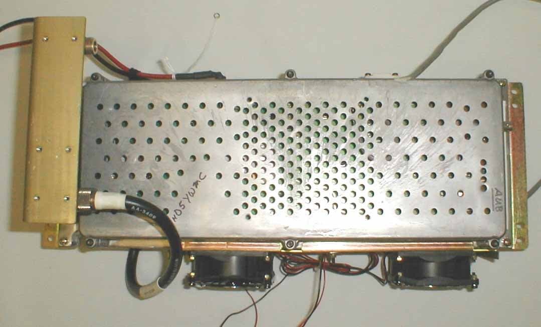
Click to zoom
Application Details
- Equipment Class
- AMP - Amplifier
- Date of Grant
- Sep 28, 2004
- Application Purpose
- Original Equipment
- Date of Application
- Sep 28, 2004
- Equipment Note
- Power Amplifier
- Frequency Range
- 851.00000000 - 870.00000000
- Country
- United States
Documents & Files
Document Text
Text extracted from the exhibit documents filed with the FCC. Open a document above to read the original.
Users Manual
Rev 2.0 6/6/04 If you have determined that the White module (U2 (STM901-30) driving the Final PA has failed... MARKII kit contains the following: 1 1ea PA assembly board 2 1ea Aluminum Spacer w/ four holes 3 4ea 3/16 #4/40 screws (for Q2 on MARK II) 4 2ea ½” #4 metric torq screws (for fastening Mark II Board & Spacer) 5 1ea FCC Label for placement on exterior of PA housing Please see B3521R3A.pdf or 19D902757G5 Mastr III PA schematic for the proper installation of this replacement module. The fan kit 188D6127G1 assembly supplied from MA/Com is required for this module for warranty to be valid. The PA will exceed heat tolerance & fail without this fan kit. Disconnect ALL power & control cable from the Mastr III Power Supply Remove U2 (STM901-30) from Power Amplifier Board A1...being careful to not damage the lands on the remaining board. Disconnect P101 from J101. (the small gold connector from the BNC input from the MIII exciter) This aids in the installation of the MARK II module. Apply heat sink compound “sparingly” to the bottom of the Aluminum Spacer Plate of the MARKII RF board. It has been proven that less is better with regards to heat sink compound. Apply only a slight amount, but sufficient to cover the surface. Align spacer plate so both holes in the circuit board of the MARK II module align for mounting. Slowly screw down each side until snug (No more than 1ft/lbs torque). Place spacer & Module into position where the U2 (STM901-30) module was previously. Mount assembly using the 4 ea. #4-40 screws. Secure all screws snug (No more than 1ft/lbs torque). Insert the module under the small hard-line coax P 101 into position & mount using all 4 screws. Be certain no excessive heat sink compound is across any connections Solder the 5 connections from the MARK II module to the pins on the Power Amp using proper RF practice. Stripped Cat5 cable lead cut to about 400 mils can be used to make your leads. Use the following U2 pin connections with the MARKKII PA. U2 PIN 12 11 6 5 2 1 MARK II RFout VDD2(A+) VG2 VDD1(A+) VG1 RFin | | | | | | It is suggested to make your pin leads bent on a 45 degree angle and soldered in the following manner making sure leads which protrude off board do not touch its own ground plane. Ex. Rfout(MarkII) Rfout(G5 Card) After inspecting that all leads are secure and all flux, etc. is cleaned off board, you are now ready for testing. Reconnect P101 to J101 Turn R1, R2, R3, R4, R204, and R48 fully counterclockwise (down approx 20 turns) (R2, & R3 will now have no effect) With all power & control cables disconnected & digital ohmmeter negative on ground : Connect 28VDC supply only (no control or drive cables) Turn 28VDC supply on (do not transmit yet ) Set Digital power PA pot on Mastr III at 97 Shut off Power Supply & connect all cables from PA to Mastr III Turn Supply back on Adjust R48 while monitoring base of Q5 (the Final) to .675 VDC Now apply PTT (Transmit) (Note: RF Power level is low...This is normal at this point of procedure!) While monitoring TP1, you should not have any control voltage. While PTT is on, slowly adjust R204 clockwise until a voltage appears on TP1 (about 0.200 VDC). Now, you have activated the knee voltage on the 22Volt regulator switch. This is needed to bias up the transistors with small signal conditions to settle in without a load, since LDMOS is very sensitive to break in voltage. Adjust R1 slowly (over at least a 20 second period) to 4.7VDC (approx 10 turns) Adjust R4 slowly (over at least a 20 second period) to 4.8VDC (approx 10 turns) Adjust R204 to approx 11 Amps or 100 watts while monitoring current and power. At this point, the amp is ready to be fielded. Place cover back on unit and remember, any digital pot setting above 95 will yield upward of 120 Watts and is not recommended nor warrentied if users go above 100 Watts of operation. Installation of Identifying Label FCC and Industry Canada Regulations require the installation of the label provided prior to operating the unit. Unit is ready for operation. Communications International, Inc. Mark II Upgrade Kit FCC ID: SA8MARKII-CII-DMD IC ID: 5363A-MARKIICA 6/3/2004 Pricing of the Mark II PA module M aster III Amplifier Replacement Kit - II stage 1. Mark II - 1-9 unit price .................................... $495 2. Mark II - 10 units or above ................................ $450 3. Mark II installed in your PA .............................. $795 4. Mark II installed in your PA with other problems ... $1495 (may include replacement with entire amplifier) Warranty Information: CII offers the following warranty on the options above. Option 1,2: 90 day warranty on parts and materials only. Each module sold from CII has been inspected, tested and burned in to produce 100 Watts before leaving the factory. CII only recommends this option to experienced communication houses who have the proper resources and experienced personnel to perform installation and test. However, if our module fails to operate during a customer installation, CII will request the customer ship back the MARK-II PA board for diagnostics to determine the problem and recommend a fix on a case by case basis. Option 3: 90 day warranty parts and labor. Shipping responsibility of customer. Option 4: 90 day warranty parts and labor. Shipping responsibility of customer. This Mark II Upgrade Kit complies with Part 90 of the FCC Rules and Regulations and Spectrum Management and Telecommunications Policy RSS-119 of Industry Canada. FCC ID: SA8MARKII-CII-DMD IC ID: 5363A-MARKIICA WARNING! Changes or modifications not expressly approved by the manufacture could void the user's authority to operate the equipment.
Cover Letter(s)
44500 US 1, Vero Beach, FL 32967 Phone: 772-569-5355 Fax: 772-978-4115 Letter Of Agency American Telecommunications Certification Body, Inc. 6731 Whittier Avenue Suite C110 McLean, VA 22101 To Whom It May Concern: Please be advised that Communications International, Inc. authorizes Washington Laboratories, Ltd. to act on our behalf, until otherwise notified, for applications submitted to American Telecommunications Certification Body, Inc. (ATCB). We certify that we are not subject to denial of federal benefits, including FCC benefits, pursuant to Section 5301 of the Anti-Drug Abuse ACT of 1988, U.S.C. 862. Further, no party, as defined in 47 CFR 1.2002(b), to the application is subject to denial of federal benefits, that includes FCC benefits. Thank you for your attention to this matter. Signed, Dale DiDomenico R.F. Engineer
Cover Letter(s)
American Telecommunications Certification Body Inc. 6731 Whittier Ave, McLean, VA 22101 September 17, 2004 RE: FCC ID: SA8MARKII-CII-DMD_ATCB001711 Attention: Gregory M. Snyder I have a few comments on this Application. Please note that further comments may arise in response to answers provided to the questions below. 1. Please note that the internal photos do not appear to show all of the boards or components. 2. Please provide internal photos showing tops and bottoms of all boards in the amplifier. Please note that the FCC ID label states, “THIS UNIT CONTAINSCommunications International, Inc.Mark II Upgrade Kit FCC ID: SA8MARKII-CII-DMD”. Please note that the FCC identifier is to be on the device certified. This statement would indicate that the FCC ID’s device is inside the product. Please explain and please show where on the FCC ID’s device the FCC ID label is to be placed and please provide a sample of the actual label that is to be on the FCC ID’s device. If the product shown in the FCC ID label exhibit is the actual device, please clarify the term “contains”. 3. Please provide a 731 which clearly identifies the emissions designators to which this device operates. (i.e. your report states ‘digital modulation’ and ‘analog’ modulation, but does not clearly identify what emissions designator is used.) Please clarify. Please clearly identify these emissions designators in the report as well (i.e. F1D, F3E, GXW, G7W etc). 4. Please note that the plots provided in the report are not clear. It is not possible to clearly identify what the plot is saying. Please provide plots that are clear. 5. Please provide intermodulation test data for this amplifier. Alternately please explain why intermodualtion tests are not required. In the case of the later, please give justification for this position. 6. Please provide an MPE report or explain why an MPE report is not needed. Please provide justification if the latter. Dennis Ward mailto:[email protected] The items indicated above must be submitted before processing can continue on the above referenced application. Failure to provide the requested information may result in application termination. Correspondence should be considered part of the permanent submission and may be viewed from the Internet after a Grant of Equipment Authorization is issued. Please do not respond to this correspondence using the email reply button. In order for your response to be processed expeditiously, you must submit your documents through the AmericanTCB.com website. Also, please note that partial responses increase processing time and should not be submitted. Any questions about the content of this correspondence should be directed to the sender.
Cover Letter(s)
Response to ATCB Comments FCC ID: SA8MARKII-CII-DMD 1 Washington Laboratories, Ltd. 7560 LINDBERGH DRIVE GAITHERSBURG, MD 20879 (301) 417 – 0220 FAX # (301) 417 - 9069 September 23, 2004 Mr. Dennis Ward American Telecommunications Certification Body Inc. 6731 Whittier Ave McLean, VA 22101 RE: Comments of September 17, 2004 APPLICATION: SA8MARKII-CII-DMD Communications International, Inc. Dear Mr. Ward: Below are the comments that you have provided regarding the application for certification referenced above. Our responses to those comments are in bold italic. Many responses refer you to additional exhibit(s) which has been uploaded to the application folder at the ATCB website. Thank you for your attention. Please feel free to contact us for any additional information that you may require. Regards, Gregory M. Snyder Chief EMC Engineer, Wireless/Telco Services Manager Brian J. Dettling Documentation Specialist WLL Project: 8188 1) Please note that the internal photos do not appear to show all of the boards or components. R. The exhibit has been upgraded to show all boards. Please see “Mark II Internal Photos Revised.pdf”. 2) Please provide internal photos showing tops and bottoms of all boards in the amplifier. Please note that the FCC ID label states, “THIS UNIT CONTAINS Communications International, Inc. Mark II Upgrade Kit FCC ID: SA8MARKII-CII-DMD”. Please note that the FCC identifier is to be on the device certified. This statement would indicate that the FCC ID’s device is inside the product. Please explain and please show where on the FCC ID’s device the FCC ID label is to be placed and please provide a sample of the actual label that is to be on the FCC ID’s device. If the product shown in the FCC ID label exhibit is the actual device, please clarify the term “contains”. Response to ATCB Comments FCC ID: SA8MARKII-CII-DMD 2 R. The phrase “This Unit Contains” has been removed from the label. Please see exhibits “Mark II Label and Location Rev 1.pdf” and “Mark II User Manual Rev 1.pdf”. 3) Please provide a 731 which clearly identifies the emissions designators to which this device operates. (i.e. your report states ‘digital modulation’ and ‘analog’ modulation, but does not clearly identify what emissions designator is used.) Please clarify. Please clearly identify these emissions designators in the report as well (i.e. F1D, F3E, GXW, G7W etc). R. As the Mark II upgrade kit is used with the MASTR III Base Station (M/A-COM FCC ID: OWDTR- 329-A2), the emission designations will be the same as for the MASTR III System (i.e. F3E, F1D, F1E, F2D and F2B). Please see exhibit “Mark II Application Form - 731 Revised.pdf”. Additionally, the test report has been revised to list these designators in Table 1. Please see exhibit “Mark II Test Report Rev 1.pdf”. 4) Please note that the plots provided in the report are not clear. It is not possible to clearly identify what the plot is saying. Please provide plots that are clear. R. The graphics have been reworked in the revised test report and the PDF conversion settings have been upgraded to allow improved clarity of the plots. 5) Please provide intermodulation test data for this amplifier. Alternately please explain why intermodulation tests are not required. In the case of the later, please give justification for this position. R. Intermodulation tests are not required as this amplifier is controlled by the MASTR III Base Station and is only connected to the single transmit output of the Base Station. Additional documentation (Maintenance Manual for the 110 Watt Power Amplifier with the MASTR III) has been provided for reference and to better explain the interface with the MASTR III Base Station. Please see exhibit “LBI-39127 Maintenance Manual.pdf”. 6) Please provide an MPE report or explain why an MPE report is not needed. Please provide justification if the latter. R. This amplifier is intended for use at fixed base station sites only. The antenna used for the base station transmitter will be fixed-mounted on outdoor permanent structures. As stated in the MASTR III Grant the RF exposure compliance is addressed at the time of licensing, as required by the responsible FCC Bureau(s), including antenna co- location requirements of §1.1307(b)(3).
External Photos
External View of MASTR III Power Amplifier
ID Label/Location Info
Label and Location Communications International, Inc. Mark II Upgrade Kit FCC ID: SA8MARKII-CII-DMD IC ID: 5363A-MARKIICA
Internal Photos
19D902797G Power Amplifier Board Mark II Upgrade Kit PCB Installed in MASTR III
Operational Description
MASTR III Operational Description Mark II Upgrade Kit Operational Description The MARKII Power amplifier amplifies a +5dbm signal to a +43dbm signal from 850MHz to 870MHz providing a bandwidth of 20MHz and gain of about 38db. It replaces another module in the MasterIII PA which is no longer available.
Schematics
BN1 W= TL2 W=115 mil L=640 mil TL4 W=115 mil L=150 mil VH1 R=15 mil BN2 W= TL1 W=115 mil L=2136 mil TL11 W=350 mil L=150 mil C1 C=3.3 pF BN3 W= (1) C10 C=100 pF C9 C=1 nF C4 C=10 uF TL13 W=115 mil L=20 mil CR1 WT=213.387 mil [wintl9i] WC=140.687 mil [wincrossi] C7 C=6.8 pF TL27i W=140.687 mil [wincrossi] L=100 mil EN5 W=140.687 mil [wincrossi] VH5 R=15 mil TL9 W=213.387 mil [wintl9i] L=581.118 mil EN3 W=150 mil CR4 WT=200 mil WC=100 mil TL5 W=100 mil L=100 mil L3 L=220 nH TP3 W1=150 mil W2=100 mil LEN=150 mil TL15 R=220 mil P=70° W=100 mil 2 1 TE1 W1= WS= TL16 W=100 mil L=325 mil Q1 File=blf1043.s2p VH10 R=15 mil VH11 R=15 mil TL7 R=220 mil P=70° W=100 mil VH6 R=15 mil EN4 W=150 mil CR5 WT=200 mil WC=100 mil 2 1 TE2 W1=115 mil WS=100 mil VH4 R=15 mil TP1 W1=150 mil W2=100 mil LEN=150 mil L4 N=3 D=157 mil L=162 mil WD=28 mil RHO=1 TL8 W=100 mil L=325 mil VH2 R=15 mil C5 C=10 uF C8 C=1 nF C2 C=100 pF VH8 R=15 mil TL12 W=100 mil L=100 mil TL10 W=350 mil L=150 mil CR2 WT=115 mil WC=100 mil VH12 R=15 mil EN2 W=100 mil TL3 W=100 mil L=150 mil C11i C=22 pF VH9 R=15 mil VH3 R=15 mil TL6 W=115 mil L=150 mil (2) 27 28 27 6 6 0 28 14 39 13 49 24 24 24 1 48 15 0 43 22 42 30 34 52 23 20 45 43 16 18 23 20 25 5 17 17 16 9 9 40 0 4 40 40 0 40 0 75 4 36 41 41 21 78 7 40 0 0 36 41 35 8 19 40 0 12 12 12 8 40 0 3 10 26 29 11 40 0 37 2 11 0
Schematics
(1) TL4 W=115 mil L=150 mil VH1 R=15 mil TL11 W=350 mil L=150 mil C1o C=?2.7 pF VH5 R=15 mil C10 C=100 pF C9 C=1 nF C4 C=10 uF CR1 WT=347.2 mil [wintl9] WC= TL5 W=100 mil L=100 mil C7o C=?4.7 pF TL27o W=?105 mil L=?167.8181 mil EN5 W=105 mil TL9o W=347.2 mil [wintl9] L=?471 mil EN3 W=150 mil CR4 WT=200 mil WC=100 mil L3 L=220 nH TP3 W1=150 mil W2=100 mil LEN=150 mil TL15 R=220 mil P=70° W=100 mil 2 1 TE1 W1= WS= TL13 W=100 mil L=325 mil R1 DISABLED: SHORT R=1000 O Q1 File=BLF1046_Spars_28V_300mA.s2p TL7 R=220 mil P=70° W=100 mil EN4 W=150 mil CR5 WT=200 mil WC=100 mil 2 1 TE2 W1= WS= VH2 R=15 mil TP1 W1=150 mil W2=100 mil LEN=150 mil L4 N=3 D=157 mil L=162 mil WD=28 mil RHO=1 TL8 W=100 mil L=300 mil C5 C=10 uF C8 C=1 nF C2 C=100 pF TL12 W=100 mil L=100 mil TL2 W=?241.6437 mil L=?351.8737 mil CR2 WT= WC=115 mil EN2 W=115 mil TL3 W=115 mil L=?150 mil C11o C=?6.8 pF TL10 W=350 mil L=145 mil C3 C=?22 pF BN1 W= TL14 W=115 mil L=780 mil VH3 R=15 mil (2) TL6 W=115 mil L=161 mil 1 0 39 13 0 24 24 24 15 33 43 22 34 17 6 52 23 20 16 18 23 20 25 5 11 16 14 41 14 4 0 44 75 4 0 36 28 28 21 78 7 36 28 35 46 19 9 46 9 12 12 12 3 10 26 29 8 37 42 2 40 32 0
Schematics
(1) TL4 W=115 mil L=150 mil VH1 R=15 mil TL11 W=350 mil L=150 mil C1o C=?2.7 pF VH5 R=15 mil C10 C=100 pF C9 C=1 nF C4 C=10 uF CR1 WT=347.2 mil [wintl9] WC= TL5 W=100 mil L=100 mil C7o C=?4.7 pF TL27o W=?105 mil L=?167.8181 mil EN5 W=105 mil TL9o W=347.2 mil [wintl9] L=?471 mil EN3 W=150 mil CR4 WT=200 mil WC=100 mil L3 L=220 nH TP3 W1=150 mil W2=100 mil LEN=150 mil TL15 R=220 mil P=70° W=100 mil 2 1 TE1 W1= WS= TL13 W=100 mil L=325 mil R1 DISABLED: SHORT R=1000 O Q1 File=BLF1046_Spars_28V_300mA.s2p TL7 R=220 mil P=70° W=100 mil EN4 W=150 mil CR5 WT=200 mil WC=100 mil 2 1 TE2 W1= WS= VH2 R=15 mil TP1 W1=150 mil W2=100 mil LEN=150 mil L4 N=3 D=157 mil L=162 mil WD=28 mil RHO=1 TL8 W=100 mil L=300 mil C5 C=10 uF C8 C=1 nF C2 C=100 pF TL12 W=100 mil L=100 mil TL2 W=?241.6437 mil L=?351.8737 mil CR2 WT= WC=115 mil EN2 W=115 mil TL3 W=115 mil L=?150 mil C11o C=?6.8 pF TL10 W=350 mil L=145 mil C3 C=?22 pF BN1 W= TL14 W=115 mil L=780 mil VH3 R=15 mil (2) TL6 W=115 mil L=161 mil 1 0 39 13 0 24 24 24 15 33 43 22 34 17 6 52 23 20 16 18 23 20 25 5 11 16 14 41 14 4 0 44 75 4 0 36 28 28 21 78 7 36 28 35 46 19 9 46 9 12 12 12 3 10 26 29 8 37 42 2 40 32 0
Test Report
Document 8188-01, Rev. 1 FCC ID: SA8MARKII-CII-DMD FCC Certification Test Report Washington Laboratories, Ltd August 2004 FCC Certification Test Report for Communications International, Inc. FCC ID: SA8MARKII-CII-DMD August 20, 2004 Prepared for: Communications International, Inc. 44500 US 1 Vero Beach, FL 32967 Prepared By: Washington Laboratories, Ltd. 7560 Lindbergh Drive Gaithersburg, Maryland 20879 FCC Certification Test Report Document 8188-01, Rev. 1 FCC ID: SA8MARKII-CII-DMD FCC Certification Test Report Washington Laboratories, Ltd August 2004 FCC Certification Test Program FCC Certification Test Report for the Communications International, Inc. Mark II Power Amplifier Upgrade Kit SA8MARKII-CII-DMD August 20, 2004 WLL JOB# 8188 Prepared by: Michael Violette President Reviewed by: Greg Snyder Chief EMC Engineer Document 8188-01, Rev. 1 FCC ID: SA8MARKII-CII-DMD FCC Certification Test Report Washington Laboratories, Ltd August 2004 ii Abstract This report has been prepared on behalf of Communications International, Inc. to support the attached Application for Equipment Authorization. The test report and application are submitted for a Power Amplifier under Part 90 of the FCC Rules and Regulations. This Federal Communications Commission (FCC) Certification Test Report documents the test configuration and test results for a Communications International, Inc. Mark II Power Amplifier. Testing was performed on an Open Area Test Site (OATS) of Washington Laboratories, Ltd, 7560 Lindbergh Drive, Gaithersburg, MD 20879. Site description and site attenuation data have been placed on file with the FCC's Sampling and Measurements Branch at the FCC laboratory in Columbia, MD. Washington Laboratories, Ltd. has been accepted by the FCC and approved by NIST NVLAP (NVLAP Lab Code: 200066-0) as an independent FCC test laboratory. The Communications International, Inc. Mark II Power Amplifier Upgrade Kit complies with the limits for a Power Amplifier device under Part 90 of the FCC Rules and Regulations. Document 8188-01, Rev. 1 FCC ID: SA8MARKII-CII-DMD FCC Certification Test Report Washington Laboratories, Ltd August 2004 iii Table of Contents Abstract ............................................................................................................................... ii 1 Introduction..............................................................................................................1 1.1 Compliance Statement .........................................................................................1 1.2 Test Scope ............................................................................................................1 1.3 Contract Information............................................................................................1 1.4 Test Dates ............................................................................................................1 1.5 Test and Support Personnel .................................................................................1 Abbreviations...................................................................................................................2 2 Equipment Under Test .............................................................................................3 2.1 EUT Identification & Description .......................................................................3 2.2 Test Configuration ...............................................................................................3 2.3 Testing Algorithm................................................................................................4 2.4 Test Location .......................................................................................................4 2.5 Measurements ......................................................................................................5 2.5.1 References........................................................................................................5 2.6 Measurement Uncertainty....................................................................................5 3 Test Equipment ........................................................................................................6 4 Test Results ..............................................................................................................7 4.1 RF Power Output: (FCC Part §2.1046) ...............................................................7 4.2 Modulation Characteristics: (FCC Part §2.1047); Audio Frequency Response ..7 Not applicable for an amplifier. ...................................................................................7 4.3 Occupied Bandwidth: (FCC Part §2.1049) ..........................................................7 4.4 Spurious Emissions at Antenna Terminals (FCC Part §2.1051) .......................15 4.5 Radiated Spurious Emissions: (FCC Part §2.1053)...........................................44 4.5.1 Test Procedure.............................................................................................44 4.6 Frequency Stability: (FCC Part §2.1055) ..........................................................46 4.7 Transient Frequency Response (Part 90.214) ....................................................46 List of Tables Table 1. Device Summary................................................................................................... 3 Table 2: Test Equipment List............................................................................................. 6 Table 3. RF Power Output .................................................................................................. 7 Table 4. Occupied Bandwidth Results................................................................................ 8 Table 5: Radiated Emission Test Data............................................................................. 45 Document 8188-01, Rev. 1 FCC ID: SA8MARKII-CII-DMD FCC Certification Test Report Washington Labo…
Text truncated - open the document above for the full version.
Contact Information
Applicant
Jamie Decker
Technical Contact
Washington Laboratories LtdGregory M Snyder
[email protected]301 417 0220
7560 Lindbergh Drive · Gaithersburg, Maryland · United States
Technical Specifications
| # | Rule Parts | Frequency Range | Power Output | Emission | Tolerance |
|---|---|---|---|---|---|
| 5 | 9 | 851 MHz - 870 MHz | 112 W | F2B | Amp |