Text extracted from the exhibit documents filed with the FCC. Open a document above to read the original.
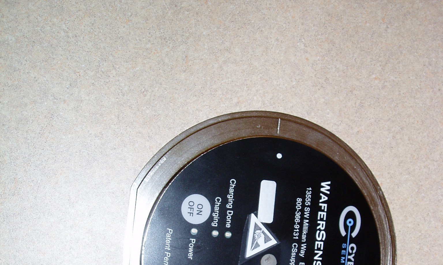
CyberOptics Semiconductor WaferSense ™ ALS150/200/300 User’s Guide ii General Information WaferSense ALS Changes or modifications not expressly approved by CyberOptics Semiconductor, Inc., may void your authority to operate the WaferSense ALS. The radio contained in the WaferSense ALS meets all the applicable FCC requirements for RF Safety. While in operation, the FCC requires users and nearby persons to maintain a minimum separation distance of 20 cm (8 inches) or farther from the WaferSense ALS. WaferSense Link Changes or modifications not expressly approved by CyberOptics Semiconductor, Inc., may void your authority to operate the WaferSense Link. The WaferSense Link has been tested and found to comply with the limits for a Class B digital device, pursuant to Part 15 of the FCC Rules. These limits are designed to provide reasonable protection against harmful interference in a residential installation. This equipment generates, uses and can radiate radio frequency energy and, if not installed and used in accordance with the instructions, may cause harmful interference to radio communications. However, there is no guarantee that interference will not occur in a particular installation. If this equipment does cause harmful interference to radio or television reception, which can be determined by turning the equipment off and on, the user is encouraged to try to correct the interference by one or more of the following measures: •Reorient or relocate the receiving antenna. •Increase the separation between the equipment and receiver. •Connect the equipment into an outlet on a circuit different from that to which the receiver is connected. •Consult the dealer or an experienced radio/TV technician for help. The radio contained in the WaferSense Link meets all the applicable FCC requirements for RF Safety. While in operation, the FCC requires users and nearby persons to maintain a minimum separation distance of 20 cm (8 inches) or further from the WaferSense Link. WaferSenseLink Tested To Comply With FCC Standards FOR HOME OR OFFICE USE iii WaferSense Technical Support Technical support is available from CyberOptics Semiconductor Monday through Friday, 8:00am to 5:00pm Pacific Time. WaferSense and LevelView are trademarks of CyberOptics Semiconductor, Inc. Third-party brands and names are the property of their respective owners. Copyright © 2003-2005, CyberOptics Semiconductor, Inc. All rights reserved. CyberOptics Semiconductor, Inc. 13555 S.W. Millikan Way Beaverton, OR 97005 P/N 920-0026-03 E-mail:[email protected] Phone:(503) 495-2200 800-366-9131 (US and Canada only) Fax:(503) 495-2201
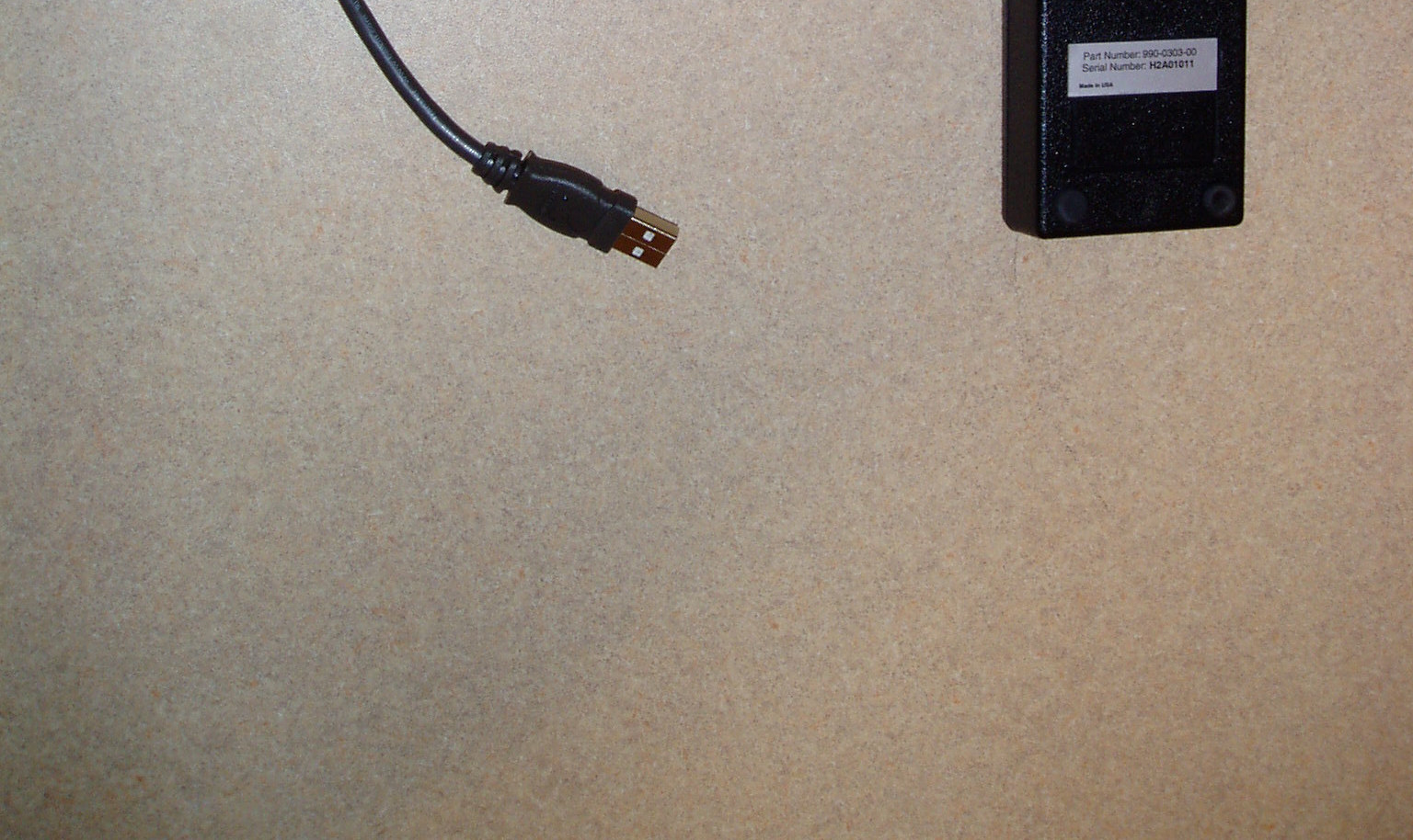
NORTHWEST EMC, INC. 22975 NW Evergreen Parkway, Suite 400 Hillsboro, OR 97124 January 15, 2005 Dear Application Examiner: On behalf of CyberOptics Semiconductor, Inc., Northwest EMC, Inc is submitting this application for the certification of CyberOptic’s WaferSense Link, FCC ID: SPD002. It contains Mitsumi’s WML-C11## Bluetooth radio module. The WaferSense Link is a USB peripheral that is used as part of a leveling system to precisely adjust manufacturing equipment. A Bluetooth-enabled level sensor is placed inside the manufacturing equipment that communicates with the WaferSense Link. The radio utilizes a single integral antenna. This configuration satisfies the requirements of 47 CFR 15.203. The digital portion of the WaferSense Link has been DoC authorized to FCC 15B. The technical reports and exhibits demonstrate compliance with FCC rules 47 CFR 15.247 as a mobile DTS transmitter. Your efforts in reviewing this application are greatly appreciated. Best regards, Greg Kiemel, Director of Engineering Northwest EMC, Inc.
Northwest EMC TCB Compliance Opinion Rev. 9/15/03 Cybr0040 Information about the Applicant Company Name CyberOptics Semiconductor, Inc. Grantee Greg Huntzinger Address 10220 SW Nimbus, Suite K5 City, State, Zip Portland, OR 97223 Job Number CYBR0040 Model WaferSense Link FCC ID SPD002 Agent Northwest EMC Approval Type Original Equipment Class DTS Digital Transmission System Rule Part Bluetooth Overview This application is for CyberOptic’s WaferSense Link, FCC ID: SPD002. It contains Mitsumi’s WML-C11## Bluetooth radio module. The WaferSense Link is a USB peripheral that is used as part of a leveling system to precisely adjust manufacturing equipment. A Bluetooth-enabled level sensor is placed inside the manufacturing equipment that communicates with the WaferSense Link. Recommendation All items have been resolved and completed to my satisfaction; therefore I recommend this application for approval. Signature 2/2/2005 Dave Tolman, TCB Committee Northwest EMC TCB Compliance Opinion Rev. 9/15/03 Cybr0040 Findings Opinions Specification Requirements Description 47 Cfr 2.1033(b)(3) Installation guide, operating instructions,user manual Opinion The device meets the requirements of the rule. Discussion The client has provided the necessary exhibit. Reference User Manual 1.pdf, User Manual 2.pdf Specification Requirements Description 47 Cfr 2.1033(b)(4) Operational description Opinion The device meets the requirements of the rule. Discussion The client has provided the necessary exhibit. Reference Operational Description public domain.pdf Specification Requirements Description 47 Cfr 2.1033(b)(5) Frequency block diagram Opinion The device meets the requirements of the rule. Discussion The client has provided the necessary exhibit. Reference Frequency Block Diagram - confidential.pdf Specification Requirements Description 47 Cfr 2.1033(b)(5) Schematic diagram Opinion The device meets the requirements of the rule. Discussion The client has provided the necessary exhibit. Reference Schematics - confidential.pdf Specification Requirements Description 47 cfr 2.1033(b)(6) Test Report Opinion The device meets the requirements of the rule. Discussion The client has provided the necessary exhibit. Reference Report-cybr0040 Rev 01.pdf Specification Requirements Description 47 Cfr 2.1033(b)(7) Internal and external photos Opinion The device meets the requirements of the rule. Discussion The client has provided the necessary exhibit. Reference Internal Photos.pdf, External Photos.pdf Northwest EMC TCB Compliance Opinion Rev. 9/15/03 Cybr0040 Specification Requirements Description 47 Cfr 1.1307(b),2.1091,2.1093 RF Exposure Hazzard Opinion The device meets the requirements of the rule. Discussion The client has provided the necessary exhibit. Reference RF Exposure.pdf Specification Requirements Description 47 Cfr 15.19 Labeling Opinion The device meets the requirements of the rule. Discussion The client has provided the necessary exhibit. Reference User Manual 1.pdf,FCC ID and Label.pdf Specification Requirements Description 47 Cfr 15.21 Information for user Opinion The device meets the requirements of the rule. Discussion The client has provided the necessary exhibit. Reference User Manual1.pdf Specification Requirements Description 47 Cfr 15.27 Special accessories Opinion The device meets the requirements of the rule. Discussion The client has provided the necessary exhibit. Reference Report-cybr0040 Rev 01.pdf Specification Requirements Description 47 Cfr 15.33 Frequency range of tests Opinion The device meets the requirements of the rule. Discussion The client has provided the necessary exhibit. Reference Report-cybr0040 Rev 01.pdf Specification Requirements Description 47 Cfr 15.35 Measurement detectors Opinion The device meets the requirements of the rule. Discussion The client has provided the necessary exhibit. Reference Report-cybr0040 Rev 01.pdf Specification Requirements Description ANSI C63.4 EUT Ports All EUT ports populated, emissions maximized, antenna height adjusted Opinion The device meets the requirements of the rule. Discussion The client has provided the necessary exhibit. Reference Report-cybr0040 Rev 01.pdf Northwest EMC TCB Compliance Opinion Rev. 9/15/03 Cybr0040 Specification Requirements Description 47 Cfr 15.203 Antenna Requirements Opinion The device meets the requirements of the rule. Discussion The client has provided the necessary exhibit. Reference Antenna Info.pdf Specification Requirements Description 47 Cfr 15.205 Restricted bands Opinion The device meets the requirements of the rule. Discussion The client has provided the necessary exhibit. Reference Report-cybr0040 Rev 01.pdf Specification Requirements Description 47 Cfr 15.207 Power line Conducted emissions Opinion The device meets the requirements of the rule. Discussion The client has provided the necessary exhibit. Reference Report-cybr0040 Rev 01.pdf Specification Requirements Description 47 Cfr 15.209 Spurious Emissions Opinion The device meets the requirements of the rule. Discussion The client has provided the necessary exhibit. Reference Report-cybr0040 Rev 01.pdf Specification Requirements Description BLUETOOTH FCC Procedure 2-15-02 Bluetooth Common Items Opinion The device meets the requirements of the rule. Discussion The client has provided the necessary exhibits. Reference Specification Requirements Description 47 Cfr 15.247(a) Occupied Bandwidth Opinion The device meets the requirements of the rule. Discussion The client has provided the necessary exhibit. Reference Report-cybr0040 Rev 01.pdf Specification Requirements Description 47 Cfr 15.247(b) Output Power Opinion The device meets the requirements of the rule. Discussion The client has provided the necessary exhibit. Reference Report-cybr0040 Rev 01.pdf Northwest EMC TCB Compliance Opinion Rev. 9/15/03 Cybr0040 Specification Requirements Description 47 Cfr 14.247(c) Band Edge Compliance Opinion The device meets the requirements of the rule. Discussion T…
Text truncated - open the document above for the full version.
Functional Description 21/May/2002 MITSUMI Bluetooth Module “ WML-C11##” Hardware:Version 1 Ultra-small and thin size achieved through use of high density mounting technology . 1. APPLICATIONS Notebook PCs, mobile phones, digital cameras, PC peripherals, PDA. 2. DESCRIPTIONS Wireless communication module conforming to Bluetooth Ver.1.1. 3. FEATURES 1 ) Ultra-small and thin size achieved through use of high density mounting technology. 2 ) High sensitivity. 3 ) UART, USB and PCMIF interfaces enable wide range of applications. 4 ) Conforms to FCC, CE and other countries’ EMI standards. 5 ) Supports Bluetooth Class1. Note)The BLUETOOTH trademarks are owned by Bluetooth SIG,INC.,U.S.A. 4. SPECIFICATIONS I t e m S p e c i f i c a t i o n s F r e q u e n c y 2402 to 2480MHz M o d u l a t i o n FHSS / GFSK Channel intervals 1 M H z Number of channels 7 9 C H Power supply voltage 3.3V(typ.) ,3.2 to 3.4V Transmission rate 7 2 1 k b p s Receive sensitivity -80dBm typ. Output level (Class1) 20dBm max. TM ©1998-2000 MITSUMI Electronics Corp. All rights reserved.MITSUMI is a trademark of MITSUMI Electronics Corporation. Other company names and products names are trademarks of their respective companies. Product specifications are subject to revisions or changes without notification. 5. TERMINAL DESCRIPTION No.SymbolI/ODescription 1GNDGround 2SPI_MOSIISynchronous Serial Interface data input (N.C.*) 3PIO [6]I/OProgrammable I/O line 4PIO [7]I/OProgrammable I/O line 5RESETIReset if high 6SPI_CLKISynchronous Serial Interface Clock (N.C.*) 7PCM_CLKI/OSynchronous PCM data clock 8PCM_SYNCI/OSynchronous data strobe 9PCM_INISynchronous PCM data input 10PCM_OUTOSynchronous PCM data out 11VDDOperating supply voltage is 3.3V+/-0.1V 12GNDGround 13UART_RXIAsynchronous Serial Data Input 14UART_TXOAsynchronous Serial Data Output 15UART_RTSOAsynchronous Serial Data RTS 16UART_CTSIAsynchronous Serial Data CTS 17USB D+USB D+ line 18USB D-USB D- line 19PIO [2] / USB PULL UPI/OProgrammable I/O line. / USB Pull-Up 20PIO [3] / USB RESUMEI/OProgrammable I/O line. / Output goes high to wake up PC when USB mode 21PIO [5]I/OProgrammable I/O line. 22PIO [4]I/OProgrammable I/O line. 23SPI_CSBIChip select for Synchronous Serial Interface (N.C.*) 24SPI_MISOOSynchronous Serial Interface data output (N.C.*) 25GNDGround 26ANTI/ORF input/output 27GNDGround 28GNDGround 29GNDGround * N.C.=OPEN **5V tolerant input terminal. 6. BLOCK DIAGRAM 7. PCM IF PCM_OUT, PCM_IN, PCM_CLK, PCM_SYNC carry one of bi-directional channel of voice data using 13bits PCM at 8ks/s. PCM_SYNC operates at a fixed clock frequency of 8kHz. PCM_CLK operates at a fixed clock frequency of 256kHz. Bits 1 to 13 of the PCM_OUT data carry the current output sample value. Bits 14 to 16 carry a three bit signal level value. Reference PCM audio device is MC145483. RF Receiver RF Transmitter 2nd Synthesizer Baseband Controller Memor y Management RAM XT Driver VDD BC2-UART / BC2-USB 1st Synthesizer 16bits Micro- Processor PIO SPI CSB SPI CLK SPI _MOSI SPI MISO SPI PCM/IF MEMORY DRIVER UART TX UART UART_RX UART _RTS UART CTS PCM OUT PCM _IN PCM _SYNC PCM CLK External- Flash ROM 256k x 16 bits PIO[2...7] BL ANT BPF 16MHz cr ystal REG RF SW PA USB D+ USB USB D- 8. OVERALL APPEARANCE Module without antenna WML-C11N# Module with antenna WML-C11A#
Compliance with 47 CFR 15.247(i) “Systems operating under the provisions of this section shall be operated in a manner that ensures that the public is not exposed to radio frequency energy levels in excess of the Commission's guidelines. See § 1.1307(b)(1) of this chapter.” The EUT is a Bluetooth radio. It will only be used with a separation distance of 20 centimeters or greater between the antenna and the body of the user or nearby persons and can therefore be considered a mobile transmitter per 47 CFR 2.1091(b). Since the transmit frequency is greater than 1.5 GHz, and the output power is less than 3.0 W ERP, the EUT is categorically excluded from routine environmental evaluation per 47 CFR 2.1091(c). The MPE estimates are as follows: Table 1 in 47 CFR 1.1310 defines the maximum permissible exposure (MPE) for the general population as 1 mW/cm 2 . The exposure level at a 20 cm distance from the EUT’s transmitting antenna is calculated using the general equation: S = (PG)/4πR 2 Where: S = power density (mW/cm 2 ) P = power input to the antenna (mW) G = numeric power gain relative to an isotropic radiator R = distance to the center of the radiation of the antenna (20 cm = limit for MPE estimates) PG = EIRP Solving for S, the maximum power density 20 cm from the transmitting antenna is summarized in the following table: The power density does not exceed 1 mW/cm 2 at 20 cm; therefore, the exposure condition is compliant with FCC rules. The applicant’s radio, FCC ID: SPD002, is compliant with the requirements of 15.247(i). MPE Estimate Antenna Type Antenna Manufacturer Antenna Part No. Transmit Frequency Max Peak Conducted Output Power Antenna Gain Minimum Antenna Cable Loss Power Density @ 20 cm General Population Exposure Limit from 1.1310 (MHz)(mW)(dBi)(dB) (mW/cm 2 )(mW/cm 2 ) ChipTDK HAN8030B2R4GT-000240034.042.1400.0111 FCC ID: SPD002
CyberOptics Semiconductor, Inc. WaferSense Link December 8, 2004 Report No. CYBR0040 Rev. 1 Report Prepared By www.nwemc.com 1-888-EMI-CERT © 2004 Northwest EMC, Inc 22975 NW Evergreen Parkway Suite 400 Hillsboro, Oregon 97124 Certificate of Test Issue Date: December 8, 2004 CyberOptics Semiconductor, Inc. WaferSense Link Emissions Specification Test Method Pass Fail FCC 15.247(a) Occupied Bandwidth:2004 ANSI C63.4:2003 FCC 15.247(b) Output Power:2004 ANSI C63.4:2003 FCC 15.247(d) Band Edge Compliance:2004 ANSI C63.4:2003 FCC 15.247(d) Spurious Conducted Emissions:2004 ANSI C63.4:2003 FCC 15.247(d) Spurious Radiated Emissions:2004 ANSI C63.4:2003 FCC 15.247(e) Power Spectral Density:2004 ANSI C63.4:2003 FCC 15.207 AC Power Line Conducted Emissions:2004 ANSI C63.4:2003 Modifications made to the product See the Modifications section of this report Test Facility The measurement facilities used to collect the data is located at: Northwest EMC, Inc. 22975 NW Evergreen Parkway, Suite 400; Hillsboro, OR 97124 Phone: (503) 844-4066 Fax: 844-3826 The sites have been fully described in a report filed with and accepted by the FCC (Federal Communications Commission) and Industry Canada. Approved By: Don Facteau, IS Manager This report must not be used to claim product certification, approval, or endorsement by NVLAP, NIST, or any agency of the federal government of the United States of America. Product compliance is the responsibility of the client, therefore the tests and equipment modes of operation represented in this report were agreed upon by the client, prior to testing. This Report may only be duplicated in its entirety. The results of this test pertain only to the sample(s) tested, the specific description is noted in each of the individual sections of the test report supporting this certificate of test. Northwest EMC Revision History Revision 05/05/03 Revision Number Description Date Page Number 01 Added “Transmitter Statement” to the Certificate of Test 2/2/2005 2 01 Removed “Northwest EMC Performance Criteria” section. 2/2/2005 6,7 Northwest EMC Accreditations and Authorizations Revision 04/01/04 FCC: Accredited by NVLAP for performance of FCC radio, digital, and ISM device testing. Our Open Area Test Sites, certification chambers, and conducted measurement facilities, have been fully described in reports filed with the FCC and accepted by the FCC in letters maintained in our files. Northwest EMC has been accredited by ANSI to ISO / IEC Guide 65 as a product certifier. We have been designated by the FCC as a Telecommunications Certification Body (TCB). This allows Northwest EMC to certify transmitters to FCC specifications in accordance with 47 CFR 2.960 and 2.962. NVLAP: Northwest EMC, Inc. is recognized under the United States Department of Commerce, National Institute of Standards and Technology, National Voluntary Laboratory Accreditation Program for satisfactory compliance with the requirements of ISO/IEC 17025 for Testing Laboratories. The NVLAP accreditation encompasses Electromagnetic Compatibility Testing in accordance with the European Union EMC Directive 89/336/EEC, ANSI C63.4, MIL-STD 461E, DO-160D and SAE J1113. Additionally, Northwest EMC is accredited by NVLAP to perform radio testing in accordance with the European Union R&TTE Directive 1999/5/EEC, the requirements of FCC, and the RSS radio standards for Industry Canada. Accreditation has been granted to Northwest EMC, Inc. under Certificate Numbers: 200629-0, 200630-0, and 200676-0. Industry Canada: Accredited by NVLAP for performance of Industry Canada RSS and ICES testing. Our Open Area Test Sites and certification chambers comply with RSS 212, Issue 1 (Provisional) and have been filed with Industry Canada and accepted. Northwest EMC has been accredited by ANSI to ISO / IEC Guide 65 as a product certifier. We have been designated by NIST and recognized by Industry Canada as a Certification Body (CB) per the APEC Mutual Recognition Arrangement (MRA). This allows Northwest EMC to certify transmitters to Industry Canada technical requirements. CAB: Designated by NIST and validated by the European Commission as a Conformity Assessment Body (CAB) to conduct tests and approve products to the EMC directive and transmitters to the R&TTE directive, as described in the U.S. - EU Mutual Recognition Agreement TÜV Product Service: Included in TUV Product Service Group's Listing of Recognized Laboratories. It qualifies in connection with the TUV Certification after Recognition of Agent's Testing Program for the product categories and/or standards shown in TUV's current Listing of CARAT Laboratories available from TUV. A certificate was issued to represent that this laboratory continues to meet TUV's CARAT Program requirements. Certificate No. USA0401C Northwest EMC Accreditations and Authorizations Revision 04/01/04 TÜV Rheinland: Authorized to carryout EMC tests by order and under supervision of TÜV Rheinland. This authorization is based on "Conditions for EMC- Subcontractors" of November 1992. NEMKO: Assessed and accredited by NEMKO (Norwegian testing and certification body) for European emissions and immunity testing. As a result of NEMKO's laboratory assessment, they will accept test results from Northwest EMC, Inc. for product certification (Authorization No. ELA 119). Technology International: Assessed in accordance with ISO Guide 25 defining the general international requirements for the competence of calibration and testing laboratories and with ITI assessment criteria LACO196. Based upon that assessment Interference Technology International, Ltd., has granted approval for specifications implementing the EU Directive on EMC (89/336/EEC and amendments). The scope of the approval was provided on a Schedule of Assessment supplied with the certificate and is available upon request. Australia/New Zealand: The National Association of Testing Authorities (NATA), Australia has been appointed by the ACA as an accreditation body to acc…
Text truncated - open the document above for the full version.
Northwest EMC Spurious Radiated Emissions Revision 10/1/03 Justification The individuals and/or the organization requesting the test provided the modes, configurations and settings available to evaluate. While scanning the radiated emissions, all of the EUT parameters listed below were investigated. This includes, but may not be limited to, antennas, tuned transmit frequency ranges, operating modes, and data rates. Channels in Specified Band Investigated: Low Mid High Operating Modes Investigated: No Hop Antennas Investigated: Integral Data Rates Investigated: Maximum Output Power Setting(s) Investigated: Maximum Power Input Settings Investigated: 120 VAC, 60 Hz. Frequency Range Investigated Start Frequency 30 MHz Stop Frequency 25 GHz Software\Firmware Applied During Test Exercise software CSR Bluetest Version 1.19 Description The system was tested using special software developed to test all functions of the device during the test. EUT and Peripherals Description Manufacturer Model/Part Number Serial Number Bluetooth Radio Link CyberOptics Semiconductor WaferSense Link H2A01012 Remote Equipment Outside of Test Setup Boundary Description Manufacturer Model/Part Number Serial Number PC Fujitsu Litebook R3Y02504 Equipment isolated from the EUT so as not to contribute to the measurement result is considered to be outside the test setup boundary Northwest EMC Spurious Radiated Emissions Revision 10/1/03 Cables Cable Type Shield Length (m) Ferrite Connection 1 Connection 2 USB Yes 3.0 No Bluetooth Radio Link PC Measurement Equipment Description Manufacturer Model Identifier Last Cal Interval Spectrum Analyzer Hewlett-Packard 8566B AAL 12/23/200313 mo Quasi-Peak Adapter Hewlett-Packard 85650A AQF 12/23/200313 mo Antenna, Biconilog EMCO 3141 AXE 12/03/200324 mo Pre-Amplifier Amplifier Research LN1000A APS 02/05/200413 mo Antenna, Horn EMCO 3115 AHC 09/07/200412 mo Pre-Amplifier Miteq AMF-4D-005180-24-10P APJ 01/05/200413 mo Pre-Amplifier Miteq JSD4-18002600-26-8P APU 10/08/200315 mo Antenna, Horn EMCO 3160-09 AHG NCR NA Antenna, Horn EMCO 3160-08 AHK NCR NA Pre-Amplifier Miteq AMF-4D-005180-24-10P APC 10/08/200315 mo Attenuator 2082-6148-20 ATE 02/03/200413 mo High Pass Filter Micro-Tronics HPM50111 HFO 04/13/200413 mo Test Description Requirement : The field strength of any spurious emissions or modulation products that fall in a restricted band, as defined in 47 CFR 15.205, is measured. The peak level must comply with the limits specified in 47 CFR 15.35(b). The average level (taken with a 10Hz VBW) must comply with the limits specified in 15.209. Configuration : The highest gain of each type of antenna to be used with the EUT was tested. The EUT was configured for low, mid, and high band transmit frequencies. For each configuration, the spectrum was scanned throughout the specified range. In addition, measurements were made in the restricted bands to verify compliance. While scanning, emissions from the EUT were maximized by rotating the EUT on a turntable, adjusting the position of the EUT and the EUT antenna in three orthogonal axis, and adjusting measurement antenna height and polarization, and manipulating the EUT antenna in 3 orthogonal planes (per ANSI C63.4:2003). A preamp and high pass filter were used for this test in order to provide sufficient measurement sensitivity. Bandwidths Used for Measurements Frequency Range (MHz) Peak Data (kHz) Quasi-Peak Data (kHz) Average Data (kHz) 0.01 – 0.15 1.0 0.2 0.2 0.15 – 30.0 10.0 9.0 9.0 30.0 – 1000 100.0 120.0 120.0 Above 1000 1000.0 N/A 1000.0 Measurements were made using the bandwidths and detectors specified. No video filter was used. Completed by: Northwest EMC Spurious Radiated Emissions Revision 10/1/03 NORTHWESTREV EMC df4.4 10/22/2004 EUT:WaferSense LinkWork Order:CYBR0040 Serial Number:H2A01012Date: Customer: CyberOptics Semiconductor, Inc.Temperature:73 Attendees:NoneHumidity:37% Cust. Ref. No.:Barometric Pressure30.11 Tested by:Rod PeloquinPower:120 VAC/60 HzJob Site:EV01 TEST SPECIFICATIONS Specification:FCC 15.247(d) Spurious Radiated EmissionsYear:2004 Method:ANSI C63.4Year:2003 SAMPLE CALCULATIONS Radiated Emissions: Field Strength = Measured Level + Antenna Factor + Cable Factor - Amplifier Gain + Distance Adjustment Factor + External Attenuation Conducted Emissions: Adjusted Level = Measured Level + Transducer Factor + Cable Attenuation Factor + External Attenuator COMMENTS EUT OPERATING MODES DEVIATIONS FROM TEST STANDARD RESULTSRun # Pass Other Freq AmplitudeFactorAzimuthHeightDistance External AttenuationPolarity Detector Distance AdjustmentAdjustedSpec. Limit Compared to Spec. (MHz) (dBuV)(dB)(degrees)(meters)(meters)(dB)(dB)dBuV/mdBuV/m(dB) Comments 4804.00065.73.3100.01.33.00.0H-HornPK0.069.074.0-5.0 Low channel 4882.00064.73.6183.01.53.00.0H-HornPK0.068.374.0-5.7 Mid channel 7440.00056.911.1113.01.33.00.0H-HornPK0.068.074.0-6.0 High channel 7440.00035.911.1113.01.33.00.0H-HornAV0.047.054.0-7.0 High channel 4882.00063.13.6125.01.13.00.0V-HornPK0.066.774.0-7.3 Mid channel 4960.00062.63.6188.01.53.00.0H-HornPK0.066.274.0-7.8 High channel 7323.00055.610.5116.01.33.00.0H-HornPK0.066.174.0-7.9 Mid channel 7323.00035.510.5116.01.33.00.0H-HornAV0.046.054.0-8.0 Mid channel 7440.00034.711.136.01.83.00.0V-HornAV0.045.854.0-8.2 High channel 7440.00054.711.136.01.83.00.0V-HornPK0.065.874.0-8.2 High channel 4804.00061.43.3359.01.23.00.0V-HornPK0.064.774.0-9.3 Low channel 7323.00033.710.545.01.33.00.0V-HornAV0.044.254.0-9.8 Mid channel 4960.00060.23.6117.01.23.00.0V-HornPK0.063.874.0-10.2 High channel 7323.00053.210.545.01.33.00.0V-HornPK0.063.774.0-10.3 Mid channel 4804.00039.63.3100.01.33.00.0H-HornAV0.042.954.0-11.1 Low channel 11/15/04 Tested By: RADIATED EMISSIONS DATA SHEET 1 No hop No deviations. 0.0 10.0 20.0 30.0 40.0 50.0 60.0 70.0 80.0 3000.0004000.0005000.0006000.0007000.0008000.0009000.00010000.000 MHz dBuV/m NORTHWESTREV EMC df4.4 10/22/2004 EUT:WaferSense LinkWork Order:CYBR0040 Serial Number:H2A01012Date: Customer: …
Text truncated - open the document above for the full version.
CyberOptics Semiconductor WaferSense ™ ALS150/200/300 User’s Guide ii General Information Technical support is available from CyberOptics Semiconductor Monday through Friday, 8:00am to 5:00pm Pacific Time. WaferSense and LevelView are trademarks of CyberOptics Semiconductor, Inc. Third-party brands and names are the property of their respective owners. Copyright © 2003-2004, CyberOptics Semiconductor, Inc. All rights reserved. CyberOptics Semiconductor, Inc. 13555 S.W. Millikan Way Beaverton, OR 97005 P/N 920-0026-02 E-mail:[email protected] Phone:(503) 495-2200 800-366-9131 (US and Canada only) Fax:(503) 495-2201 iii Tab l e o f Contents General Information ......................................................ii Chapter 1 Introduction ....................................................................................1.1 Chapter 2 Installing Your ALS....................................................................... 2.1 Installing the Software .................................................................... 2.1 Installing the Wireless Link............................................................2.3 Checking the Link to the Sensor ....................................................2.4 Registering Your Sensor for Calibration Service ............................2.4 Running the LevelView Application ..............................................2.5 Technical Support ..........................................................................2.6 Chapter 3 Using Your ALS ............................................................................. 3.1 Using the ALS Sensor Buttons and Status Lights..........................3.2 Performing a Basic Inclination Measurement ...............................3.3 Alignment Marks ...................................................................................... 3.6 Setting the Stabilization Criteria ....................................................3.7 Setting the Go/No Go Tolerance...................................................3.8 Specifying a Reference Plane ....................................................... 3.10 Monitoring the Operating Temperature ...................................... 3.12 Logging Your Readings ............................................................... 3.13 Automatic and Manual Logging ........................................................... 3.14 Including User-Specified Information in the Log File ..................... 3.15 Working in a Different Time Zone ..................................................... 3.15 Changing the Log File............................................................................ 3.15 Displaying Readings from a Log File .................................................. 3.16 Table of Contents iv Printing the LevelView Window................................................... 3.17 Using the Rechargeable Battery................................................... 3.18 Monitoring the Battery Level................................................................ 3.18 Charging the Battery .............................................................................. …
Text truncated - open the document above for the full version.
| # | Rule Parts | Frequency Range | Power Output |
|---|---|---|---|
| 1 | 15C | 2.40 GHz - 2.48 GHz | 34.00 mW |

WaferSense ALS
Equipment Class
DTS - Digital Transmission System