SXT6M-1K26M HIGH POWER AMPLIFIER
M2 ANTENNA SYSTEMS INC.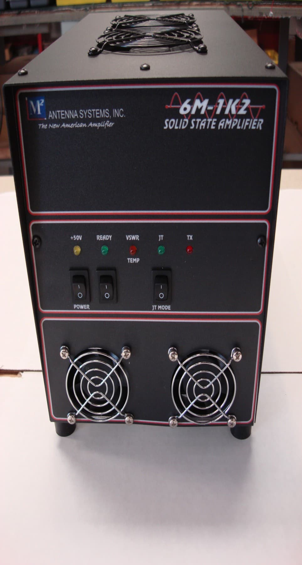
Click to zoom
Application Details
- Equipment Class
- AMP - Amplifier
- Date of Grant
- May 14, 2013
- Application Purpose
- Original Equipment
- Date of Application
- May 14, 2013
- Equipment Note
- 6M HIGH POWER AMPLIFIER
- Frequency Range
- 50.00000000 - 54.00000000
- Company
- M2 ANTENNA SYSTEMS INC.
- Country
- United States
Documents & Files
Document Text
Text extracted from the exhibit documents filed with the FCC. Open a document above to read the original.
Users Manual
4/18/13 Rev.02 PLEASE READ BEFORE USE AND SAVE TROUBLESHOOTING OVERVIEW INSTALLATION ADDENDUM WARRANTY M2 Antenna Systems, Inc. Model No: 6M-1K2 6M High Power Amplifier Operating Instructions M2 Antenna Systems, Inc. 4402 N. Selland Ave. Fresno, CA 93722 Tel: (559) 432-8873 Fax: (559) 432-3059 Web: www.m2inc.com ©2011 M2 Antenna Systems Incoporated 2 CONTENTS SECTION........................................................... PAGE COVER PAGE ........................................................ 1 CONTENTS ........................................................... 2 OVERVIEW ........................................................... 3 Introduction ................................................. 3 Features ...................................................... 3 Major Components........................................ 4 Theory of Operation...................................... 6 INSTALLATION...................................................... 8 Typical Installation Diagram........................... 8 Installation Considerations............................. 8 TROUBLESHOOTING ............................................. 9 Troubleshooting Guide .................................. 9 Support, Service and Returns ........................ 10 Schematic Diagram ....................................... 11 ADDENDUM .......................................................... 12 Parts List...................................................... 12 Specifications ............................................... 13 WSJT: What Is It and How Do I Get It? .......... 14 WARRANTY .......................................................... 16 M2 Antenna Systems, Inc. 4402 N. Selland Ave. Fresno, CA 93722 Tel: (559) 432-8873 / Fax: (559) 432-3059 http://www.m2inc.com ©2011 M2 Antenna Systems Incoporated OVERVIEW 3 OVERVIEW OVERVIEW It is with great satisfaction that M 2 now offers a true breakthrough in high power VHF amplifiers. Our goal has always been to offer the most carefully designed, high performance antenna products. Now we offer the same high performance in VHF amplifiers. The 6M-1K2 and the 2M-1K2 utilize the new Freescale™ LD MOS FET (MRFE6VP6IK25H), a single device specified to produce 1.25 kW with as little as 3 watts of drive from HF to 600 MHz. This is amazing in itself, but adding its inherent stability driving that power into a 65:1 mismatch is equally incredible. It can do all this at efficiencies well above 60%! YOU CAN SEE WHY WE ARE EXCITED! Here is where M 2 comes in. We wanted to make it small and we did; 6 x 7.125 x 13.5 inches (152 x 181 x 343 mm) so it will fit in a suitcase. We wanted it to be light and it is at just 13 lbs (5.9 kg). The optional integrated 2400 watt switching power supply adds only another 7.5 lbs to this incredible package that travels easily at 20.5 lbs (9.3 kg). Additionally, the power supply may be purchased as a separate, stand alone accessory. Now, at home in your shack you won’t need that big steel rack any more. All you need is a small desktop or shelf to hold your QRO (high power) VHF amplifier. Above all we made this amplifier easy to understand and operate. The photo below shows the model with the amplifier and the power supply integrated together (7.125” wide, 9” high 14” deep). INTRODUCTION By now you may realize that there is a lot more in this amplifier package than just a 1.25 kW LDMOSFET. What you can’t see in pictures is listed proudly below: • A complete and accurate high power VSWR bridge. • Regulator PC board with high wattage power resistors and two voltage regulators. • Medium power input power coaxial relay. • High power, high speed vacuum relay easily capable of handling full output power. • Monitoring via high accuracy DC current and temperature monitoring devices. • Sophisticated output RF filter reducing spurious harmonics to exceed FCC regulations. • Quiet fan on the bottom cools miniature RF tank and filter components. • 50 or 100 watt input attenuator that reduces your input power to safe drive levels. FEATURES Frescale™ is a registered trademark of Freescale Semiconductor, Inc. 4 OVERVIEW MAJOR COMPONENTS, 6M-1K2 FRONT PANEL 1. +50V LED (Yellow). Indicates +50 VDC is present from the power supply 2. Ready LED (Green). Lights when the Power switch is on and the amplifier is ready to be keyed and driven. 3. VSWR/TEMP LED (Amber). When lit, indicates an excessive VSWR condition (2.5:1 or greater) at the output, or when the amplifier is overheating. 4. JT Mode LED (Green). Lights when the JT switch is on or within 5 seconds after driving the amplifier in FM, AM or JT mode with the JT Mode switch off. 5. TX LED (Red). Indicates the amplifier is keyed to TX (transmit). 6. AC Power On/Off Switch. (PS equipped models only.) Turns AC power on and off to the integrated power supply. 7. Power Switch. Puts the amplifier in the Ready-to-Key state. When off, the amplifier is bypassed. 8. JT Mode Switch. Puts the amplifier in JT mode. When in JT mode, the amplifier changes to near Class “C” opera- tion, running cooler and more efficiently for continuous duty modes. OVERVIEW 1 2 3 4 5 6 7 8 5 OVERVIEW REAR PANEL (shown with optional power supply) 9. Key Jack. Ground to transmit. The total keying current is under 10 mA. 10. RF In. 50-80W nominal, 100W max. 11. RF Out. It is strongly recommended that an external wattmeter be connected here. Use .405” or larger diameter, 50 ohm coaxial cable capable of handling full rated output power. RG-213, LMR-400 or similar cables are suitable. 12. Terminal Strip. Provides connections for fans, +13.6 VDC for powering external device and key out for external relay and preamp switching. 1. +28VDC top cover fan voltage. 2. Fan voltage return. 3. External relay key return (48 VDC max.) used to key external, optional components. 4. +13.6 VDC @ 500 ma max for external relays and preamp. 5. Chassis ground. 13. External AC Power Cord. Included only on models equipped with integrated power supply. For models without the …
Text truncated - open the document above for the full version.
Block Diagram
4/10/2013 JK RF Design 8441 Diane Ct. Gilroy, CA 408-842-0616 Rev. A M2 ANTENNA SYSTEMS INC. 6M-1K2 Block Diagram KEYING HIGH SWR HIGH TEMPERATURE SHUT DOWN VOLTAGE REGULATORS +50 IN +50 OUT +13.6 INT +13.6 EXT TO FANS 50 VOLT POWER SUPPLY FAN CONTROL FANS BIAS BYPASS JT MODE CONTROL TEMPERATURE CONTROL TEMPERATURE DETECTOR OUTPUT MATCHING NETWORK LOWPASS FILTER OUTPUT RELAY SWR DETECTOR Q1 MRFE6VP61K25HR6 INPUT MATCHING NETWORK 28 MHz TRAP GAIN ADJUST INPUT RELAY RF IN RF OUT KEY
External Photos
APPLICANT: M2 ANTENNA SYSTEMS INC. FCC ID: SXT6M-1K2 EXTERNAL PHOTOS
Operational Description
6 The 6M-1K2 designation, indicates the amp works on the 6 meter Amateur Band and is capable of at least 1.25 kW of RF output. A single MRFE6VP61K25H Freescale™ LDMOSFET solid state device is the heart of the amplifier. Because most modern Amateur transceivers have a 50 to 100W output on 6M, the gain of the device must be reduced 15 dB or less per part 97 FCC rules. The input level is dropped to 4 to 5 watts so the device is not overdriven as fatal damage will occur. In “bypass mode” or with the Ready switch off and the green LED un lit, the input RF passes through an input relay and then through a high power vacuum relay, through the internal SWR bridge and out to the antenna. When the Ready/power switch is activated and the green LED is lit, the Amplifier can be keyed and when driven with the rated RF drive, will amplify to at least 1200 Watts into 50 Ohms. The Keying circuit requires a path to ground or near ground through the RCA connector on the rear of the amplifier. This is usually accomplished by the transceiver but can also be keyed with a foot switch. A built in 15 to 20 millisecond delay al- lows the relays to close before a +2.8 VDC bias voltage is applied to the gates of the device. When “keyed up”, with no drive applied to the device, it will idle at approximately 2 amps. This condition puts the device in a class AB1 state. It is linear at this point so a drive of 5W will cause the amp to produce 100+Watts. On 6M, 100W of drive, in SSB or CW mode will allow the amplifier to produce 1200 Watts minimum. If the drive power is continuous such as with AM, FM or any JT mode, the amplifier will sense this continuous drive level and after about 5 seconds, the bias voltage is reduced pulling the amplifier closer to class C. This reduces the drain current typically from 36 amps down to about 30 Amps and reduces the output slightly to 950 to 1050 Watt output. When driven in the Single Sideband mode SSB or CW, the amplifier runs in the linear mode and delivers 1250W+peak to the antenna. At full drive level the amp is at about the 1 dB compression point. Further drive will not cause much more output, just more compression, possible distortion and less efficient operation. A temperature sensor mounted next to the device, monitors the Celsius temperature of the huge copper “heat spreader” the device is attached to. When the device temperature reaches about 40 degrees C, the two large but very quiet fans on the top cover come on to push the warm air transferred to the aluminum fins out the rear of the amp. Another slightly smaller, quiet bottom fan comes on and pushes cool outside air into and over the device and other RF components. This warm air vents out the multiple rectangular openings at the rear of the main chassis. Over temperature occurs at 90 deg. C and the amber LED will light. Cycling the READY switch re-sets the system. A complete 1500W+ VSWR bridge is located just inside the RF output connector hear the rear panel. Forward and reflected power is monitored and if the SWR reaches 2.5:1, the control system de-activates the amplifier and the AMBER LED on the front panel will light. This “fault” condition can be “reset” easily by cycling the “Ready” switch or removing the 50 VDC powering the unit. Operation in the fault condition is possible by turning off the ready switch and running in the “amp bypass” mode at the drive level of your transceiver. When 50 VDC enters the amplifier, it is split and one part passes through a 3 Amp fuse on the rear panel. this 50V DC is sent to the regulator board and accompanying power dropping resistors for fans and two voltage regulators where 13.6 volts is produced for the control board functions and other relay operation. The 50 VDC is also sent through 0.005 ohm resistor in the drain lead of the device. The voltage drop across the 0.005R is sensed and conditioned to provide a linear voltage related directly to the device current in a 1/10 ratio. 10 Amps of drain current reads out as 1.00 volts and 30 Amps of drain current reads out as 3.00 volts. This circuit allows accurate FACTORY ADJUSTMENT of Idle current, and secondary bias control for JT, AM, or FM mode of operation. The RF drive power from a transceiver enters through an “N” female connector on the rear panel and jumpers through a THEORY OF OPERATION OVERVIEW OVERVIEW 7 small 50 Ohm coax to a medium power relay followed by the 100W power attenuator. Then the RF passes through an im- pedance matching network and coaxial transformer and on to the gates of the device. Bias voltage also passes through the transformer. The emitter of the device is grounded to its flange base (header) which in turn is attached to the copper heat spreader. There is a common ground then in the system between the chassis, the PC board and the heat sink system. This ground connection is very important for heat transfer and also for total device stability and current flow. On the output side of the device, lar ge PC board traces provide high power, high current connections to two cross-connected 10 ohm coax line sections. These line sections form a 9:1 Impedance step and transform the very low drain impedance up to about 25 ohms, balanced. A high current dc ferrite choke brings the 50 VDC to the drain sides of the device. Various tuning, blocking and bypassing capacitors aid in the balanced tank circuits transition through a coax line to a 50 ohms, unbalanced point. Following the tank circuit is a seven section low pass filter. The filter is followed by a high power vacuum relay, the VSWR bridge and finally the output ‘N’ female connector. 6M-1K2 BLOCK DIAGRAM OVERVIEW OVERVIEW
Schematics
8/25/2012 JK RF Design 8441 Diane Ct. Gilroy, CA 408-842-0616 Rev. F Amp Control Board DIAGRAM R5 33K + C2 1uf C1 .01uf C1b .01uf C1c .01uf C1a .01uf R3 100 R2 10K R1 1.2K R4 1.8K D1 914 D1a 914 Q1 MPS2907 + - +13.6 C3 .01uf R6 10K R9 10K R12 560 R7 3.0K R8 7.5K R13 2.2K FANS TX RY 7 5 6 8 U1 LM2904 U1 R11 1K R14 2.2K R15 2.2K R16 100K + - 1 3 2 4 R10 1.0K Q8 MPSA29 Q15 ZTX601 D22 1N914 SWR 2 SWR 6 D18 BAT46 J7 J7 J7 6 5 7 8 - + R21 2.4K R23 33K R22 100 R19 22K R18 10K R20 6.8K U2 LM2904 2 3 1 - + C10 .01uf C8 .01uf C11 .01uf C9 .01uf C12 .33uf R24 68K R25 1.8K R26 8.2K R28 8.2K R27 560 R29 100K C13 2.2uf D8 LED D17a,b LED Q6 2N5062 Q7 MPS2907 C14 .01uf +13.6 + +13.6 R62 0 +13.6 +13.6 +13.6 U5 LM2902 U5 U5 2 3 1 - + A R33a 68K C20 1000 C21 1000 C23 1000 C31 .01uf C35 .01uf C34 .01uf C30 .01uf C33a 1000 BD675 Q10 5551 D11 LM4040 2.5v J7 D9 914 R46 470K R45 2.2K R63 0 R64 0 C26 33uf R47 5.6K Q11 MPS A13 R40 220 R39 1.5K R50 500 R51 1.5K R52 300 R38 20K J7 +5V SET J7 JT DISABLE 6 5 7 - - + + + C16 1000 C32 1000 C15 1000 C38 1000 C39 1000 C C24 .01uf +13.6 + - +13.6 R33 1.2K C19 .01uf C19a .01uf R35 47 R36 47 R37 2.2K + - 14 12 13 8 10 9 11 4 C R31 10K R31a 1000 U3 LM2902 U3 U3 R32 10K R34 10K + - 1 3 2 11 4 C17 .01uf C18 .01uf +13.6 LM 35 ON TX BOARD ON TX BOARD R60 FS R61 560 2M 6M SW2 JT SSB/CW SWR HI TEMP HIGH SWR SENSOR J6 Q1 BIASQ2 BIASFWR PWRREV PWRTEMPKEY+13.6 +13.6 SW3 J3 JT ONON+50SWR/TEMPGND GND Id Q1Id Q2 JT DISABLE 5v SET J1 ON REAR PANEL J3 J2 J7 KEY KEY KEY, BIAS, ANT RELAY, FANS SEQUENCER and EXT RELAY OUTPUT AGC & JT SELECT REGULATORS & FAN RESISTOR TEMPERATURE SENSOR FAN & SHUT DOWN CONTROL 1000w SET 5v SET FAN DELAY NOT USED R30R43 LAST NUMBERon this SHEET U5RY1SW3 R64 Q15J8D22 C39 A B B D2 BAT46 Q4 ZTX601 JP1 RY1 for Dual Band Q5 5551 Q9 2N5551 Q3 ZTX601 Q2 ZTX601 D6 SB1100 D7 1N3070 A B 11 R48 2.2K R48a 2.2K Q13 5551 Q14 5551 Q12 5551 D10 LED JT R49 3.3K J7 J7 +13.6 EXT RY R54 200 JP1-1 BAND JP3-1 BAND JP2=2 XISTOR R55 470 R57 470 R56 200 D12 BAT46 BIAS 1 BIAS 2 10 4 2 3 144 144 J3 J8 50 50 13 5 6 7 1112 R53 2.2K C29 .01uf C29a .01uf U4 LM723 R17 560 D4 LED J6 BIAS SET TX FAN + FAN+ J3 FAN - TB +13.6 EXT +13.6 EXT D3 1N3070 D5 1N3070 C25 1000 C27 .01uf R44 18K R42 100K R41 220 5 7 - - + + C22 1000 B 4 +13.6 C6 1000 C7 .01uf C28 .01uf C37 1000 C28a .01uf C36 1000 C4 1000 B1 FAN J4 C5 2.2uf + + - J7 D13 BAT46 D16 LED READY +13.6 R59 560 +13.6 C33 .01uf 5 12 14 13 D14 LED D15 1N5938 J7 +50 J7 ON R58 560 +50 READY POWER SW1 SW3 J7 F A N + J4 J3 +50 J3 +13.6 INT J3 +13.6 EXT A A C8a 1000 FWD C8b 1000 C8c 1000 FWD C8d 1000 REV REV RY1a RY1b +13.6 RY1 D21 BAT46 D20 BAT46 D19 BAT46 J7 J8 J3 R31 R18 R20 R55 R57 R27 SW3 2/6 C26 C25 D1 J6 J3 FAN - EXT RY J3
Schematics
+50 F1 3A RF IN RF OUT FB1 FB2 C4 1000pF C1 .01uf TX J2 BIAS 1 Q1 MRFE6VP61 C3 47uf C2 6.8uf R3 11 T1 B1 T2 R6 5.1K R4 10K R5 10K L3 FS L4 1T C11 .01uf C10 2.2uf C23 90 TO +50 D3 1N5357 C12 1000C13 1000C14 1000 C20 1000C21 1000C22 1000 C9 .01uf C8 2.2uf C7 10uf C33 .01uf R7b 1500 5w (4v = 40A) 1/17/2013 JK RF Design 8441 Diane Ct. Gilroy, CA 408-842-0616 Rev. P RF SECTION 6M-1K2 Six Meter Amp RY1 W2 W1 R1 40 12 3 REV FWD SEE SWR DIAGRAM RY2 C27 1000 C26 40 C28 1000 L5 3T L6 3T L7 3T TX RX C24 80 C25 80 C5 470uf C6 470uf TO RY2 +50 Idq C31 1000 FB3 C30 1000 C32 1000 C29 .01uf U2 MAX 4080 1 8 2 5 4 C36 .01uf U1 R9 51 C35 0.22uf +13.6 TO R31 TO D11 LM 35 C34 .01uf FB4 Q2 BD675 TX J1 TX J1 TX J1 TX J2 R2 10 L2 .33uh L2a FS L1 FS C1b 100pf C1a FS C1c FS C37 1000 C38 1000 D2 1100 LAST NUMBER NOT USED C38D3FB4L7Q2R9RY2U2W2 TX RX 13.6V C15 .01ufC16 .01ufC17 1000pfC18 2.2mfdC19 2.2mfd C1d 1000pF C1e .033uf R7 .010 R7a .010 R8 0 D1 6A1
Schematics
RF in RF out J2 T1 D1 1N6263 R1 33 R3 470 R4 470 R5 100K R6 100K R2 33 D2 1N6263 C4 39 C6 FS 6/23/2011 JK RF Design 8441 Diane Ct. Gilroy, CA 408-842-0616 Rev. I SWR BOARD C7 1000 C9 .01uf C8 1000 C10 .01uf C1 4.7 500v C222 C310 C5 3.3 L1 8.2uh REV FWD
Schematics
4/3/2011 JK RF Design 8441 Diane Ct. Gilroy, CA 408-842-0616 Rev. K 13.6 VOLT REGULATOR/FAN M2 INTERNAL & EXTERNAL 13.6v REGULATORS AND FAN DROPPING RESISTOR LAST NUMBERon this SHEET C6R7U2 FAN + +13.6 EXT + EXTERNAL +13.6 R7 2.37K R9 2.37K C6 2.2uf 25v R8 243 TL783 U2 C5 .01uF + C4 1uf 50v R6 50 30W R5 FS 15W + INTERNAL +13.6 R2 2.37K C3 2.2uf 25v R3 243 R4 2.37K U1 C2 .01uF + C1 1uf 50v R1 50 30W +50 +13.6 INT TL783
Test Report
FCC PART 97 AMATEUR RADIO TEST REPORT Applicant M2 ANTENNA SYSTEMS Address 4402 N. SELLAND AVENUE FRESNO CA 93722 USA FCC ID 6M-1K2 Model Number 6M-1K2 Product Description 6M HIGH POWER AMPLFIER Date Sample Received 4/18/2013 Date Tested 5/14/2013 Tested By Nam Nguyen Approved By Mario de Aranzeta Report Number 658AUT13TestReport.doc Test Results PASS FAIL THE ATTACHED REPORT SHALL NOT BE REPRODUCED EXCEPT IN FULL WITHOUT THE WRITTEN APPROVAL OF TIMCO ENGINEERING, INC. 849 NW State Road 45 Newberry, FL 32669 USA Phone: 888.472.2424 or 352.472.5500 Fax: 352.472.2030 Email: [email protected] Website: www.timcoengr.com Certificate # 0955-01 APPLICANT: M2 ANTENNA SYSTEMS FCC ID: 6M-1K2 REPORT: M\M2 ANTENNA\658AUT13\658AUT13TestReport.doc Page 2 of 17 TABLE OF CONTENT STATEMENT OF COMPLIANCE ................................................................................................. 3 GENERAL INFORMATION .......................................................................................................... 4 EMC EQUIPMENT LIST .............................................................................................................. 6 TEST PROCEDURES: ................................................................................................................. 7 RF POWER OUTPUT .................................................................................................................. 8 IN BAND GAIN ........................................................................................................................... 9 OUT OF BAND GAIN ................................................................................................................ 12 STRENGTH OF SPURIOUS EMISSIONS ................................................................................... 13 POWER LINE CONDUCTED INTERFERENCE .......................................................................... 14 FCC EXPOSURE INFORMATION .............................................................................................. 17 APPLICANT: M2 ANTENNA SYSTEMS FCC ID: 6M-1K2 REPORT: M\M2 ANTENNA\658AUT13\658AUT13TestReport.doc Page 3 of 17 STATEMENT OF COMPLIANCE This equipment has been tested in accordance with the standards identified in the referenced test report. To the best of my knowledge and belief, these tests were performed using the measurement procedures described in this report and demonstrate that the equipment complies with the appropriate standards. No modifications were made to the equipment during testing in order to demonstrate compliance with these standards. I attest that the necessary measurements were made by me or under my supervision, at TIMCO ENGINEERING, INC. located at 849 N.W. State Road 45, Newberry, Florida 32669 USA. Tested by: Nam Nguyen Signature: Function: Testing Tech/Project Manager Date: May 15, 2013 Authorized by: Signature: Mario de Aranzeta C.E.T. Compliance Engineer/ Lab. Supervisor Date: May 15, 2013 APPLICANT: M2 ANTENNA SYSTEMS FCC ID: 6M-1K2 REPORT: M\M2 ANTENNA\658AUT13\658AUT13TestReport.doc Page 4 of 17 GENERAL INFORMATION DUT Specification The test results relate only to the items tested. DUT Description 6M HIGH POWER AMPLFIER FCC ID 6M-1K2 Model Number 6M-1K2 Serial Number N/A Operating Frequency 50 to 54 MHz Testing Frequency 50.5 and 53.5 MHz Type of Emission J3E, F3E, A3E Modulation FM, AM, SSB DUT Power Source 180–264VAC/50– 60Hz DC Power (48-50 VDC, 40A) Battery Operated Exclusively Test Item Prototype Pre-Production Production Type of Equipment Fixed Mobile Portable Antenna Connector N connector Supporting Peripheral Equipment HF/VHF/UHF Transceiver Model: IC-706MKIIG Manufacture: Icom Inc. Modifications to DUT: No Yes (explanation below) Adding to the AC power line: 1. FN9246-12-06 Filter 2. Two ferrites (part #43 material) APPLICANT: M2 ANTENNA SYSTEMS FCC ID: 6M-1K2 REPORT: M\M2 ANTENNA\658AUT13\658AUT13TestReport.doc Page 5 of 17 Test Facility: The test sites used by Timco Engineering Inc. for radiated and conducted emission data are located at 849 NW State Road 45 Newberry, FL 32669 USA. Test Condition: The DUT was tested in the laboratory in an environment with normal temperature and humidity. The temperature was 26ºC with a relative humidity of 50%. Modification to the DUT: No modification was made to the DUT during testing. Test Exercise (e .g software description, test signal, etc.): The DUT was placed in continuous transmit mode of operation . Applicable Standards: TIA 603 & ANSI C63.4 – 2003 FCC CFR 47 Part 97 FCC CRF 47 Part 15 Other information: The amplifier is capable of operation in the amateur radio 6 meter band (50-54 MHz). The amplifier is NOT capable of operation on any frequency or frequencies between 26 MHz and 28 MHz as marketed. 1.. The amplifier requires 80 Watts of drive to obtain full output power. Reduction in RF input power reduces the output power as shown on Page 8. 2. The gain of the amplifier is under 15 dB and under all conditions. 3. The amplifier in the off or standby state does not amplify and merely passes through the exciter energy to the antenna port. The spurious emissions of the transceiver were unaffected. APPLICANT: M2 ANTENNA SYSTEMS FCC ID: 6M-1K2 REPORT: M\M2 ANTENNA\658AUT13\658AUT13TestReport.doc Page 6 of 17 EMC EQUIPMENT LIST Device Manufacturer Model Serial Number Cal/Char Date Due Date 3-Meter Semi- Anechoic Chamber Panashield N/A N/A 12/31/11 12/31/13 AC Voltmeter HP 400FL 2213A14499 6/12/11 6/12/13 Hygro- Thermometer Extech 445703 0602 6/15/11 6/15/13 Digital Multimeter Fluke FLUKE-77 35053830 9/9/11 9/9/13 DC Power Supply Astron VS-50M 9001191 01/19/13 01/19/15 Power Meter Boonton Electronics 4531 11793 1/9/13 1/9/15 Sensor Boonton 51072A 34647 01/19/13 01/19/15 Attenuator Bird 8329-300 4980 2/26/13 2/26/15 EMI Receiver Rohde & Schwarz ESIB40 100274 3/16/12 3/16/14 Analyzer Tan Tower Preamplifier HP 8449B-H02 3008A00372 10/28/11 10/28/13 Analyzer Tan Tower Quasi- Peak Adapter HP 85650A 3303A01…
Text truncated - open the document above for the full version.
Contact Information
Applicant
MICHAEL STAAL(CFO)
Test Firm
Timco Engineering, Inc.Bruno Clavier
Technical Specifications
| # | Rule Parts | Frequency Range | Power Output | Emission | Tolerance |
|---|---|---|---|---|---|
| 1 | 97 | 50 MHz - 54 MHz | 1250 W | XXX | Amp |