TBMRTX2-U2DATA TRANSCEIVER
D-Tek Electronics, Inc.
Click to zoom
Application Details
- Equipment Class
- TNB - Licensed Non-Broadcast Station Transmitter
- Date of Grant
- Jun 27, 2005
- Application Purpose
- Original Equipment
- Date of Application
- Jun 27, 2005
- Equipment Note
- DATA TRANSCEIVER
- Frequency Range
- 440.00000000 - 470.00000000
- Company
- D-Tek Electronics, Inc.
- Country
- United States
Documents & Files
Document Text
Text extracted from the exhibit documents filed with the FCC. Open a document above to read the original.
Users Manual
RTX2-U2 LINK MODULE 2005.03.08. page-17- RTX2-U2 PROGRAMMING INTRODUCTION Using the RTX2-U2 PC programming cable and software gives access to all programmable functions and features. The RTX2-U2 programmer enables you to: • Customise RTX2-U2 radio to your own requirements • Input new settings, frequency data • Read the settings of an already existing RTX2-U2 and store these data as files. • Clone channel and other important information from one radio to another • Gain access to a range of other product features RTX2-U2 LINK MODULE 2005.03.08. page-18- GETTING STARTED When you receive your RTX2-U2 PC programming kit, make sure the following items are included: • RTX2-U2 software (on 3.5" disk) • Programming cable TO RUN THE RTX2-U2 SOFTWARE The programmer works on most IBM compatible PCs. However, the minimum software and hardware requirements you need to run RTX2-U2 successfully are: DOS 3.0 or later 512K Bytes of memory One parallel port HARDWARE CONNECTION: IMPORTANT! In order to access the programmer connentor, you need to take off the upper cover. To do so, unscrew the four upper mounting screws located on the upper cover of the radio. With the PC switched off, connect the programming cable /25-way D type connector/ to a vacant parallel communication port on the PC /typically on to the PC printer port /, and the 5- poled end of the programming cable to the programming socket of the RTX2-U2 transceiver. For a smooth performance we suggest installing the RTX2-U2.exe directly onto the computer's hard disk. It will require approximately 400K of disk space. Running software from hard disk : The programming of the equipment is to be done while it is switched off. / without external Power Supply / Start running the RTX2-U2. exe . PROGRAMMING A RADIO The programming screen consist of the following: RTX2-U2 LINK MODULE 2005.03.08. page-19- SETTINGS CHANNEL DATA You can set 16 transmitter-receiver frequency-pairs in the 440-470 MHz band. Selection of channels: with the up/down arrows. You can select TX power either High: 2W or Low: 0.5 W for each of the channels. RTX2-U2 LINK MODULE 2005.03.08. page-20- PARAMETER RX/TX in / PTT / A: the transmission starts on low level /0 V/ B: the transmission starts on high level /+5V/ Where: Low level: <1V High level: >3.5V-15V SCAN : FREE CHANNEL Starting from channel 1 / or which has the lower channel number/ it will search for a free channel among the preset channels. preset channels: where both TX and RX frequency are set. BUSY CHANNEL Starting from channel 1/ or which has the lower channel number/ it will search for a busy channel among the preset channels. NONE The receiver will use the channel data, which is set by the DIPswitch. BUSY CHANNEL LOCKOUT If selected, you can only start sending a message if there is no present busy signal in the given channel. RTX2-U2 LINK MODULE 2005.03.08. page-21- RASTER 5 kHz The preset channels are located on a 5 kHz raster 6.25 kHz The preset channels are located on a 6.25 kHz raster TX TIME OUT Limits the amount of time that the user can continuously transmit /can be set from 10 seconds to 990 second / DROP OUT In SCAN FREE and SCAN BUSY CHANNEL mode the drop out time of the presence or absence of the busy detect signal can be set between 4-510 msec. /drop out time as result, the equipment will step on the next channel. / PROGRAMMING PORT SETTING Here you can select which computer-port to connect the programming cable to. /LPT1.2, 3/ RTX2-U2 LINK MODULE 2005.03.08. page-22- LOAD WRITE This command programs the radio according to the above parameters. Note: On programming a radio, all the information previously contained in the RTX2-U2 will be lost. READ The preset values/data can be checked or read from the settings of an already existing RTX2-U2. /for cloning/ RTX2-U2 LINK MODULE 2005.03.08. page-23- FILE menu NEW The input of new data . SAVE The preset data can be saved as bin. files Type in the filename under which the data is to be saved . OPEN Open a saved bin. files Radio data alredy saved to disk can be loded into the PC. EXIT FCC RF EXPOSURE STATEMENT To maintain compliance with FCC’s RF exposure guidelines, this equipment should be installed and operated with minimum distance of 20 cm. between the radiator and your body. Use only the supplied antenna.
Block Diagram
162738495 D-SU B 9J1 +12VHF_ INRSSIDBUSY_DPTTCHSHFO GN D R-T. RTX2-U2 BLOCK DIAGRAM 200 5.02.0 7. AN T. LPF D8 D9 AN T SW LPF RF DET. D1 0 P.A.Q1 8 Q1 7 Q1 1 Q9 ,10 L1 2 T8 V +12V AN T SW AUTOMATIC POWER CONTROL CIRCUIT P1 IC4A ,B Q2 0 , Q5 T8 V DT R SQR/PWR TX BUFFER POWER ADJUST RX/TX VCO LPF PLL SYNTHESIER TCXO 12 .8 MHz +5V X6 IC1 LMX2 31 6 +5V TU N Mod R/T LO CA L L PF Q1 3 RX BUFER MIXER IC3AD E1 FILTE R FILTE R PREAMP. Q1 +5V 1s t IF FILT ER IF PREAMP Q1 2 45 MHz IC2 BA4116 2nd LOCAL45.545MHz CERAMIC FILTER 455 KHz X1 QADRATU RE L3 4 R5V R5V HF IF FILTC33,34 R72 DE MPH ASIS C30/R38 JP3 AU DIO AMP IC2/A HFO RESET IC5 EE PRO M IC6 IC4 AT98C2051 +5V+5V +5V RSSI CIR. Q7 ,8 RSSI /BUSY CIR. IC3 RSSID BUSY_D P2 RSSI LEV EL ADJ UST +12V +8V +5V DIP SW IT CH CH SEL. BUSY_IN BUSY_IN CHSPTT JP1 PROGRAM . CON. CPU +5V R5V R/T +5C SW ITCHI NG C.1 Q1 9,Q 4 R/T +8V T8 V +5C SW ITCHI NG C.2 Q2 1,1 5, D4 DT R HF_ IN IC10/A MO D.PRE AM P. PREEMPHASIS JP1 R5/C12 LIMITE R IC1/A TX LPF IC1B/C/D MOD IC878 M08 IC7 78 L0 8 LD CLK DA TA LE 12 .8 MHz APPENDIX page 1
External Photos
RTX2-U2 LINK MODULE 2005.03.08. page-3- RTX2-U2 LINK MODULE 2005.03.08. page-9- INTRODUCTION The RTX2-U2 Link Module allows radio frequency signals to be used for the control of electrical equipment, building security systems, monitoring stations,emergency call-boxes and much more. The RTX2-U2 radios are comprised of two PCB's (an RF-PCB and an Control-PCB). These boards are connected with an 16 pin female and male connector . The control board is interfaced with external data equipment through the 9 pin d-sub male connector, which controls the radio and data receiving and sending . The radios are programmed using an IBM® Personal Computer, a DOS® based software, and a programming cable. This allows the radio to be tailored to meet the requirements of the individual user and of the System(s) it is operating within.
ID Label/Location Info
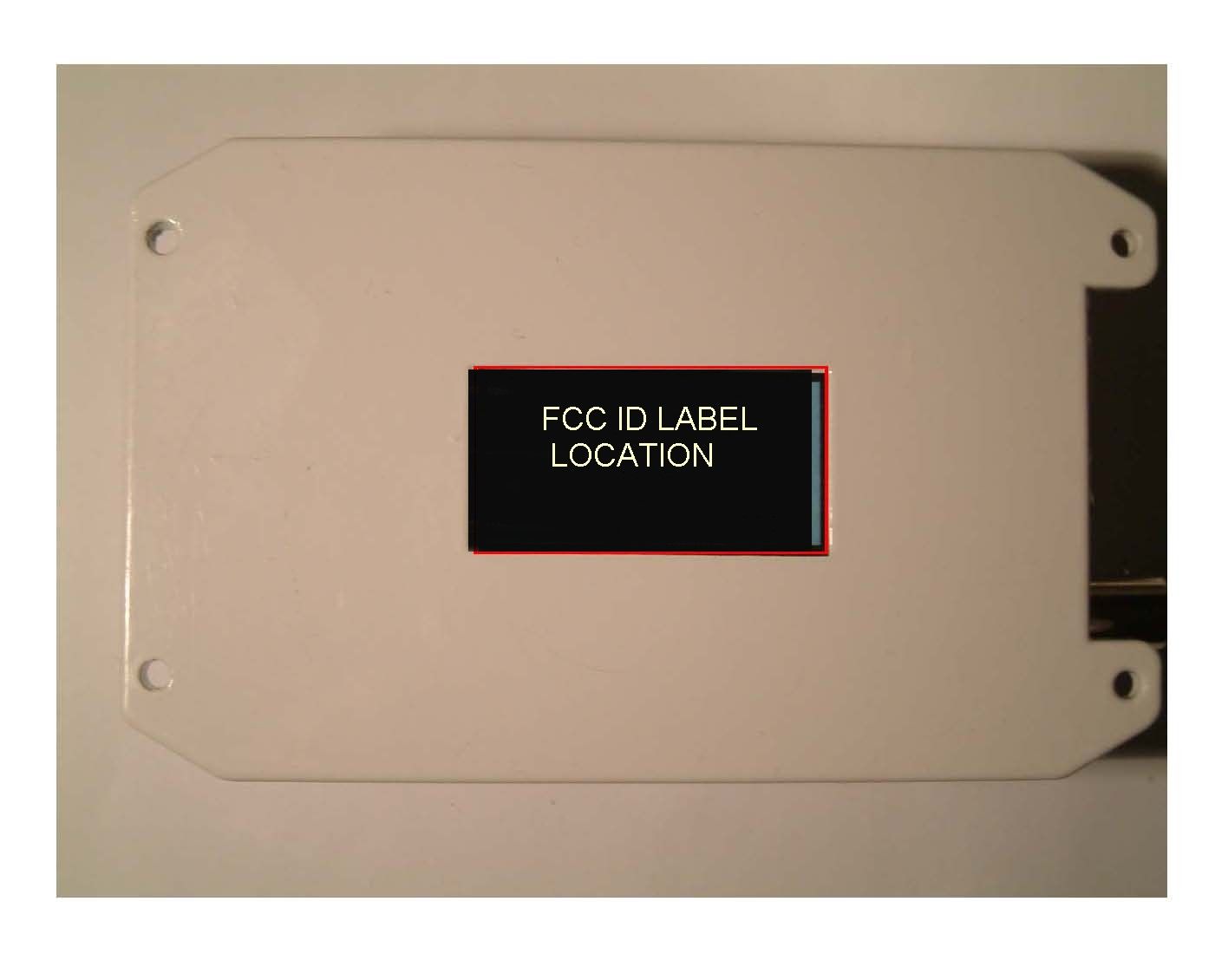
_________________________ . FCC ID: TBMRTX2-U2. This device complies with part 15 of the FCC Rules.Operation is subject to the conditions that this device does not cause harmful interference D-Tek Electronics Inc. Los Angeles California 90025
Internal Photos
RTX2-U2 LINK MODULE 2005.03.08. page-11- THEORY OF OPERATION CIRCUITS on the RF- PCB TRANSMITTER CIRCUITS: • BUFFER Amplifier VCO output level is approx. +1dBm and amplified to +23dBm by the buffer amplifier. The buffer consists of Q9,10 as a cascade and of Q11,17 between a resistive divider / R6,7,8 / for the required isolation and gain. • POWER AMPLIFIER The Power Amlifier is Q18. The amplifier amplifies the TX signal from +23 dBm to 2W matched to 50 Ohms using a microstrip L and C105,110 network, thereby reducing the Fig.1 Fig.2 RTX2-U2 LINK MODULE 2005.03.08. page-14- The output of the post filter amplifier, Q12, is coupled via C47 to the input of IC2 ( BA4116). IC2 is a monolithic single conversion FM IF system, containing a mixer, the second local oscillator, limiter and quadrature detector. Crystal X2 / 44.545 MHz / is used to provide resultant 455kHz signal from the output of the second mixer. The mixer output is then routed to X1 (CFW455G). These ceramic filters provide the adjacent channel selectivity of 12,5 kHz bandwidth. RSSI ( RECEIVER SIGNAL STRENGTH INDICATOR ) The RSSI signal is output from IC2 on pin 12. As the receiver signals the output, DC voltage is varied as much as receiver signal strength. CIRCUITS ON THE CONTROL-PCB EEPROM RX / TX channel and as well as other data from the programmer are stored in the EEPROM. The stored data is retained without power supply. This is a non-volatile and re-programmable memory. IC6 is an EEPROM with 4096 (8 x 128) capacity and data is written and read serially. CHANNEL SELECTOR One of 16 channels may be selected using the Dip Switch (IC9) and serial commands. The hardware selector, IC9 encodes the channel number, selected into 4-bit binary code. The binary code plus one equals the channel number. The binary code is decoded by the MCU, which enables the appropriate RX or TX frequency and associated data to be selected from the EEPROM. The external serial channel stepping command comes from Pin 9 of the DB-9 / J1/ connector and enhances the actual channel number by one.
Operational Description
RTX2-U2 LINK MODULE 2005.03.08. page-11- THEORY OF OPERATION CIRCUITS on the RF- PCB TRANSMITTER CIRCUITS: • BUFFER Amplifier VCO output level is approx. +1dBm and amplified to +23dBm by the buffer amplifier. The buffer consists of Q9,10 as a cascade and of Q11,17 between a resistive divider / R6,7,8 / for the required isolation and gain. • POWER AMPLIFIER The Power Amlifier is Q18. The amplifier amplifies the TX signal from +23 dBm to 2W matched to 50 Ohms using a microstrip L and C105,110 network, thereby reducing the RTX2-U2 LINK MODULE 2005.03.08. page-12- harmonics by -30 dB. • HARMONIC FILTER Chebyshev low pass filter. Unwanted harmonics are reduced by -70 dBc. • ANTENNA SWITCH When transmitting, the diodes D8 and D9 are forward biased to enable to make an RF path to the antenna. D9 is shorted to ground to block the RF signal to the front-end. In receive, the diodes, D8 and D9, are reverse biased to pass the signal from the antenna through L29 and C62 to the front-end without signal loss . APC CIRCUIT The APC (Automatic Power Control) circuit provides a stable power output. Detector D10 rectifies the forward signals, and produces a d. c. level which is directly proportional to the RF output power level. The detected voltage is applied to pin 6 of amplifier IC4B. P1 sets d. c. voltage to the other input (pin 5) as a reference. This reference voltage is controlled by the MCU too (across Q5,R41). / High or Low power / IC4B determines the RF power level by producing a difference signal. The difference signal is passed to Q16, Q22 to produce a constant power output by controlling the voltage supply rail to amplifier Q17. The required power output is set by adjusting P1. The output of IC4A adjusts Q11 basis bias, and set the required drive level characteristic in compliance with the transient behaviour of the transmitter. PLL SYNTHESIZER : • 12.8 MHz TCO The applied temperature compensated crystal oscillator offer excellent temperature characteristics with low power consumption and fast warmup. Compensation is ±2.5ppm or less from -30c to +60c. • PLL IC DUAL MODULES PRESCALER Input frequency of 12.8 MHz to IC1 LMX2316 pin 8 is divided to 6.25 kHz or 5 kHz by the reference counter, and then supplied to the comparator. RF signal input from VCO is divided to 32/33 at the prescaler in IC1, divided by A and N counter in IC1 to determine frequency steps, and then supplied to the comparator. PLL comparison frequency is 6.25/5kHz so that minimum programmable frequency step is 5/6.25 kHz. RTX2-U2 LINK MODULE 2005.03.08. page-13- The A and N counter is programmed to obtain the desired frequency by serial data in the MCU. In the comparator, the phase difference between reference and VCO signal is compared. The Charge Pump Output of IC1 connected to a loop filter for driving the input of the VCO. Combined with a high quality reference oscillator and loop filter, the LMX2316 provide the feedback tuning voltage for a voltage controlled oscillator to generate a low phase noise local oscillator signal. • REFERENCE FREQUENCY LPF The Loop Filter contains R66,69,33, C97 and C100. LPF settling time is 12mS with 1 kHz frequency. This also reduces the residual side-band noise for the best signal-to-noise ratio. • VCO The VCO’s operating frequency range can be switched by the D2 and D3 switching diodes according to the transmit or receive mode. It is controlled by the MCU. The VCO is configured as a colpits Oscillator(Q6) . It’s connected to the buffer, which a cascade amplifier /Q7,8/. The varicap diode D5 is a low- resistance element and produces a change in frequency with a change in reverse bias voltage (1-4,5V). L15 is a resonant coil, which changes the control voltage by the tuning core. The VCO is modulated by the audio signal through D6 modulation diode. By connecting to the VCO’s tuning voltage, the circuit of R93,34,C139 compensates for the non-linearity of the VCO due to modulation diode, and maintains a constant modulation regardless of frequency. RECEIVER FRONT-END The receive signal is routed backward through the low pass filter, then onward to the input of the Receiver Front End. It consists of a bandpass filter (C1 through C14, L 1 through L3) which is coupled to the base of Q1 which serves as an RF amplifier. Diode D1 serves as a protection from static RF overload from nearby transmitters. The output of Q1 is then coupled to a second bandpass filter consisting of C16 through C23 and L4 through L7. The output of Front End is then coupled to the double balanced mixer IC3. FIRST MIXER The double balanced mixer generates the 45 MHz intermediate frequency output from RF and local frequency. The 45MHz IF output is matched with the input of the 4-pole monolithic filter by L13, C124 and C101. The crystal filter provides a bandwidth of ±7.5 kHz at the operating frequency for a high degree of spurious and inter-modulation protection. The IF filter provides additional attenuation for the image frequency of the second mixer. The output impedance of the filter is matched with the base of the post amplifier Q12 by C115. SECOND OSCILLATOR MIXER LIMITER AND FM DETECTOR RTX2-U2 LINK MODULE 2005.03.08. page-14- The output of the post filter amplifier, Q12, is coupled via C47 to the input of IC2 ( BA4116). IC2 is a monolithic single conversion FM IF system, containing a mixer, the second local oscillator, limiter and quadrature detector. Crystal X2 / 44.545 MHz / is used to provide resultant 455kHz signal from the output of the second mixer. The mixer output is then routed to X1 (CFW455G). These ceramic filters provide the adjacent channel selectivity of 12,5 kHz bandwidth. RSSI ( RECEIVER SIGNAL STRENGTH INDICATOR ) The RSSI signal is output from IC2 on pin 12. As the receiver signals the output, DC voltage is varied as much as receiver signal strength. CIRCUITS ON THE CONTROL-PCB EEPROM RX / TX channel and as well as other data from the programmer are stored in the EEPROM. The stored data is retained without p…
Text truncated - open the document above for the full version.
Parts List/Tune Up Info
RTX2-U2 LINK MODULE 2005.03.08. page-24- TRX2-U2 CONTROL-PCB PARTS LIST NOTESDesignatorCommentFootprint C14n7060310% X7R C24n7060310% X7R C34n7060310% X7R C44n7060310% X7R C54n7060310% X7R C64n7060310% X7R C74n7060310% X7R C8100n060320% Z5U C91u080520% Z5U C101u080520% Z5U C111n060310% X7R C122n2060310% X7R C131u080520% Z5U C141u080520% Z5U C1522p06035% NP0 C1610n060310% X7R C1710n060310% X7R C18100n060320% Z5U C1910n060310% X7R C2010n060310% X7R C21220n060320% Z5U C22100n060320% Z5U C23100n060320% Z5U C241n060310% X7R C251n060310% X7R C26100n060320% Z5U C271n060310% X7R C281n060310% X7R C29100n060320% Z5U C3022n060310% X7R C311uF080520% Z5U C32220p06035% NP0 C33100n060320% Z5U C341n060310% X7R C3522uTANTAL B size6V 20% C3610n060310% X7R C37220p06035% NP0 C38220p06035% NP0 C39220p06035% NP0 C40220p06035% NP0 RTX2-U2 LINK MODULE 2005.03.08. page-25- C41220p06035% NP0 C42220p06035% NP0 C43220p06035% NP0 C44220p06035% NP0 D1BZV55 5V6SOD80 D2BZV55 5V6SOD80 D3LL4148SOD80 D4SA15A1812 IC1LM324SOIC 14 IC2TL062SOIC 8 IC3LM393SOIC 8 IC4AT98C2051SOICW 20 IC5MCP130-450I/TTSOT-23 IC624LC00SOIC 8 IC778L05SOIC 8 IC878M08DPACK IC9SWITCH 4XSOICW 8 IC10TL062SOIC 8 J1D-SUB 9DB9SLWMale JP1MOLEX5325353253 JP2PRINTED JUMPER JP3PRINTED JUMPER JP6HEADER 16BERG 16PIN P21k3374X Q1DTC114WUSOT-323 Q2DTC114WUSOT-323 Q3DTC114WUSOT-323 Q4DTC114WUSOT-323 Q5DTC114WUSOT-323 Q6DTC114WUSOT-323 Q7BC847BSOT-23 Q8BC857BSOT-23 Q9DTA114WUSOT-323 Q10BFR93ASOT-23 Q11DTA114WUSOT-323 Q12n.f.SOT-23 Q13n.f.SOT-23 Q14n.f.SOT-23 R110k06035% R210k06035% R310k06035% R410k06035% R510k06035% R610k06035% R727k06035% R847006035% R910k06035% RTX2-U2 LINK MODULE 2005.03.08. page-26- R1010k06035% R1110k06035% R1210k06035% R1310k06035% R1410k06035% R1510k06035% R1610k06035% R1710k06035% R1810k06035% R1910k06035% R2010k06035% R214k706035% R224k706035% R234k706035% R244k706035% R254k706035% R264k706035% R274k706035% R282k206035% R294k706035% R304k706035% R311k06035% R324k706035% R33470k06035% R3475k06035% R3547k06035% R3647k06035% R37220k06035% R3847k06035% R3947k06035% R401k06035% R41220k06035% R42220k06035% R43220k06035% R44220k06035% R458k206035% R46470k06035% R479k106035% R4810006035% R4910006035% R5010006035% R5110k06035% R521k06035% R538k206035% R541k06035% R552k206035% R56n.f.06035% RTX2-U2 LINK MODULE 2005.03.08. page-27- R57n.f.06035% R58n.f.06035% R595606035% R605606035% R6122k06035% R624k706035% R6322006035% R64006035% R65n.f.06035% R66220k06035% R67006035% RTX2-U2 LINK MODULE 2005.03.08. page-28- TRX2-U2 RF - PCB PARTS LIST NOTESDesignatorCommentFootprint C59n.f.0603 C118n.f.0603 C123n.f.0603 C149n.f.0805 D7n.f.SOD80 R21n.f.0603 R7800603 R90n.f.0603 R91n.f.0603 R60112065% P11k3374X R41k06035% R101k06035% R111k06035% R121k06035% R191k06035% R291k06035% R721k06035% R791k06035% R811k06035% R331k206035% R891k308051% R241k506035% C391n060310% X7R C401n060310% X7R C411n060310% X7R C471n060310% X7R C491n060310% X7R C1141n060310% X7R C931p06030,5pF NP0 C991p06030,5pF NP0 C1481p06030,5pF NP0 D21SS356SOD-323 D31SS356SOD-323 C1021u080520% Z5U C1031u080520% Z5U C672-6pPOT-C R502k206035% R672k206035% R682k206035% R252k706035% RTX2-U2 LINK MODULE 2005.03.08. page-29- R322k706035% R652k706035% R923k08051% C1043p306030,5pF NP0 R304k706035% R314k706035% L14meIND SMD 604T,i.d.:1mm L24meIND SMD 604T,i.d.:1mm L34meIND SMD 604T,i.d.:1mm L44meIND SMD 604T,i.d.:1mm L54meIND SMD 604T,i.d.:1mm L64meIND SMD 604T,i.d.:1mm L74meIND SMD 604T,i.d.:1mm C174p06030,25pF NP0 C864p706030,5pF NP0 C874p706030,5pF NP0 C1094p706030,5pF NP0 C1124p708050,25pF NP0 C1334p706030,5pF NP0 C1344p706030,5pF NP0 C1194u7TANTAL A size10V 20% C585p606030,5pF NP0 C605p608050,25pF NP0 D11BZV55 5V6SOD80 D12BZV55 5V6SOD80 D13BZV55 5V6SOD80 D14BZV55 5V6SOD80 R666k806035% C76p806030,25pF NP0 C86p806030,25pF NP0 C216p806030,25pF NP0 C256p806030,5pF NP0 C426p806030,5pF NP0 C626p806030,5pF NP0 C1056p808050,5pF NP0 C1176p806030,5pF NP0 C37p06030,25pF NP0 C47p06030,25pF NP0 C57p06030,25pF NP0 C858p206030,5pF NP0 C1088p206030,5pF NP0 C1468p206030,5pF NP0 R71006035% R561006035% R571006035% R581006035% R591006035% RTX2-U2 LINK MODULE 2005.03.08. page-30- R611006035% R310k06035% R2010k06035% R8310k06035% R9510k06035% C4610n060310% X7R C4810n060310% X7R C5410n060310% X7R C6910n060310% X7R C7010n060310% X7R C7110n060310% X7R C7210n060310% X7R C7310n060310% X7R C7410n060310% X7R C7610n060310% X7R C7810n060310% X7R C7910n060310% X7R C8010n060310% X7R C8410n060310% X7R C12210n060310% X7R C13510n060310% X7R C13710n060310% X7R C14410n060310% X7R C14510n060310% X7R C110p06035% NP0 C1910p06035% NP0 C3010p06030,5pF NP0 C5610p06030,5pF NP0 C6310p06030,5pF NP0 C6510p08050,25pF NP0 C6610p08050,25pF NP0 C8310p06030,5pF NP0 C11110p08050,25pF NP0 C211p06035% NP0 R5212k06035% R5312k06035% R5412k06035% R5512k06035% C2012p06035% NP0 C4412p06035% NP0 X512.8MHzTCXO 7 R915k06035% R7515k06035% C615p06035% NP0 C2315p06035% NP0 C5315p06035% NP0 C10615p06035% NP0 RTX2-U2 LINK MODULE 2005.03.08. page-31- C10715p06035% NP0 C12615p06035% NP0 R6918k06035% R7318k06035% R7418k06035% L2318nHIND MINI SPRING L2618nHIND MINI SPRING L2718nHIND MINI SPRING L2818nHIND MINI SPRING L2918nHIND MINI SPRING C1318p06035% NP0 C1818p06035% NP0 C12418p06035% NP0 C1220p06035% NP0 C10120p06035% NP0 C432206035% R222212065% R632206035% R3522k06035% R3722k06035% R3822k06035% R3922k06035% R4022k06035% C8122n060310% X7R C10022n060310% X7R C14722n060310% X7R L1822nH08055% L1922nH08055% L2022nH08055% L2122nH08055% L2422nH08055% L3022nH08055% L3122nH08055% C3122p08055% NP0 C13622p06035% NP0 C924p06035% NP0 R127k06035% R4127k06035% C5727p06035% NP0 C14027p06035% NP0 C1030p06035% NP0 C1430p06035% NP0 C1530p06035% NP0 C2230p06035% NP0 R6433nH06035% C1133p06035% NP0 C6433p06035% NP0 RTX2-U2 LINK MODULE 2005.03.08. page-32- C11633p06035% NP0 C11533p06035% NP0 C12733p12065% NP0 X244,545MHzHC80 X345G7B1HC80-3 X445G7B1HC80-3 R54706035% R844706035% R3447k06035% R7147k06035% R9347k06035% L2247nH08055% C3247p06035% NP0 C11047p08055% NP0 R775606035% R885606035% C12556p0…
Text truncated - open the document above for the full version.
Parts List/Tune Up Info
Measurement of RTX2-U2 The control board must be tested with an appropriate tester which controls the IC4 microcontroller and the modulating amplifier. The RF-board must be measured with a previously tested control-panel. Start the measurement in “receive” position. Check the current consumption (the +12V power supply’s current consumption including the control panel). The current consumption must be 100mA ± 5% . Tune coil L15 in such way that the voltage at test point MP1 be greater than 1V @ 440MHz, smaller than 4.5V @ 470MHz. Setting of the front-end circuit: By tuning coils L1,L2,L3,L4,L5,L6,L7 we obtain an amplification peak between 8-10dB in a frequency range between 440-470MHz, a waviness in this band smaller than 2dB and a damping more than 70dB @ a frequency range between 340-380MHz.. Setting of the discriminator circuit: Connect the rf modulation signal with U=50uVemf , devation=1.5kHz(peak) , f=1kHz. Measure the output signal at the control panel’s J1 connnector’s pin number 2. Tuning the coil L34 we get the max. amplitude. Measure the unit’s sensitivity on three frequencies, 440,455 and 470MHz. The sensitivity must be better than 0.3uV @ 50ohm,12dB SINAD Measurement in TX position: Connect an appropriate instrument (measurement of 50 ohm impedance power output) to the unit’s rf connector. Put the control panel in TX mode. The current consumption can not be more than 1A @ +12V. Tune condensator C67 in such way that the voltage at test point MP1 be greater than 1V @ 440MHz, smaller than 4.5V @ 470MHz . Turn the P1 potentiometer counterclockwise until end stand. Put the control panel in HIGH POWER position. Measure the output power @ frequencies 440,455,470MHz with +10V power supply. If necessary correct the power output level with TJ1 and TJ2. The measured power output after 10 seconds must be at least 2W on the above mentioned three frequencies With the same HIGH POWER setting, but with +12V power supply and @ 455MHz, set the output power to 2W with the help of potentiometer P1. Then measure the power output @440 and 470MHz.. The variations from 2W of the measured values must not exceed 1dB. Now put the control panel in LOW POWER position and measure the output power @ frequencies 440,455,470MHz. The measured values must be 0.5W ± 1dB Assemble the RF unit and the control unit. Check the modulation in TX mode. . Apply 1Vpp 1kHz signal to pin 1 of connector J1. On a measuring receiver you must get a 1.5kHz+/-10% deviation. In RX mode set up the "BUSY DETECT" circuit: from a signal generator apply to the input a signal sufficient to obtain a 20db SINAD On the control panel turn the potentiometer P2 counterclockwise until end stand, then slowly turn it clockwise until the signal at J1 connector’s pin 6 turns from logic 1 to logic 0.
Schematics
10 kR1 10 kR2 4n 7C1 4n 7 C2 10 kR3 10 kR4 4n 7C3 4n 7 C4 MOD 23 4 1 11 LM32 4 IC1A 56 7 LM32 4 IC1B 8 9 10 LM32 4 IC1C 1213 14 LM32 4 IC1D 10 kR5 10 k R6 27 kR7 4k 7R21 10 kR9 10 kR10 10 k R11 10 kR12 10 kR13 4n 7C5 4n 7 C6 4k 7R22 10 kR14 U/ 2 2n 2C12 47 0kR33 +8VK HF_ IN DT C Q1 R/T 1kR40 1kR31 75 kR34 22 0kR37 47 0R8 10 0nC8 47 kR39 +8VK 22 0kR41 1nC11 1 2 3 HE AD ER 3JP2 32 1 84 TL 06 2 IC10A 10 kR15 22 0pC32 1u FC31 +8V 22 0k R44 22 pC15 9k 1R47 8k 2R45 22 0nC21 HF 10 0R48 10 kR51 1uC10 U/ 2 HFO 47 kR38 22 nC30 1 2 3 HE AD ER 3JP3 1u FC9 32 1 84 TL 06 2 IC2A 22 0kR66 56 7 TL 06 2 IC2B 22 0kR4222 0kR43 +8V 1uC13 10 nC16 1uC14 10 nC17 U/ 2 Q1 3 Q1 2 Q1 4 R56 R57R58 R65 +5V +8V +8VK 0 R64 R/T 32 1 84 LM39 3 IC3A 56 7 LM39 3 IC3B +5V 47 0kR46 4k 7R23 1nC24 4k 7R24 +5V 8k 2R531kR54 +5V 1nC25 RSSI1 10 kR1610 kR17 +5V 4k 7R25 +5V BUSY_DBUSY_IN 10 0R49 1nC27 BFR93A Q1 0 10 kR20 22 0R63 +5V 1nC28 12 .8 MH z TCX O BC847Q7 10 kR18 +5V 10 kR19 BC857Q8 +5V RSSI1 10 0R50 RSSID +12V +8V +5V DT R R/T SQR/PWR MOD TCX O RSSI1 HF LD LE DA TA CLK 12345678910111213141516 HE AD ER 16JP6 22 uC35 0R67 1nC34 R-T. RTX2-U2 SCHEMATIC DIAGRAM 200 5.02.0 7. part CONTR1- 1kP2 APPENDIX page 6 123456789 10 11121314151617181920 AT 98 C2 05 1IC4 DT CQ2 DT CQ3 DT CQ4 DT CQ5 4k 7R26 4k 7R27 2k 2R28 +5V +5V +5V R/T25 /1 2.5 kSQR/PWR12 .8 MH z 1kR52 4k 7R29 PTT +5V 5V 6D1 4k 7R30 DT CQ6 DT R +5V DT AQ9 +5V 10 0nC22 Vd d 2 GN D 3 RST 1 MCP130 -45 0I/T TIC5 10 0nC23 56R59 +5V 56R60 +5V 10 0nC26 LD LE DA TA CLK A0 1 A1 2 A2 3 Vs s 4 SDA 5 SCL 6 WP 7 Vcc 8 24 LC00IC6 22 k R61 4k 7 R62 47 kR35 41 48D3 +5V 47 kR36 12345 MOLE X5 32 53JP1 2k 2R55 +5V 5V 6D2 4k 7R32 BUSY_INCHS 1234 5678 78 L0 5IC7 +8V 10 0nC29 10 0nC18 +5V 1 2 3 45 6 7 8 SWITCH 4XIC9 DT AQ1 1 10 0nC33 162738495 D-SU B 9J1 +12VHF_ INRSSIDBUSY_DPTTCHSHFO GN D 10 nC19 10 nC20 +12V D4 1 2 3 In Out 78 M08IC8 4n 7C7 +8V +12V +8V +5V DT R R/T SQR/PWR MOD TCX O RSSI1 HF LD LE DA TA CLK 12345678910111213141516 HE AD ER 16JP6 22 uC35 0R67 1nC34 R-T. RTX2-U2 SCHEMATIC DIAGRAM 200 5.02.0 7. part CONTR2- 10 nC36 22 0pC38 22 0pC44 22 0pC37 22 0pC39 22 0p C43 22 0pC40 22 0p C41 22 0p C42 +12VHF_ INRSSIDBUSY_DPTTCHSHFO APPENDIX page 7 REC_IN FEO 10 pC1 11 pC2 7pC3 7pC4 7pC5 24 pC9 4meL1 30 pC10 33 pC11 20 pC12 4meL2 4meL3 BAS-70D1 30 pC14 27 kR1 BFR93AQ1 10 0R2 4meL4 47 0pC16 R5V 4pC17 10 pC19 12 pC20 15 pC6 6p 8C7 6p 8C8 18 pC18 6p 8C21 30 pC22 30 pC15 18 pC13 15 pC23 4meL5 4meL6 4meL7 10 nC137 ncR79 56R88 MP 1 2 3 4 5 6 7 89 10 11 12 13 14 15 16 BA4116 IC2 33 pC116 6p 8C117 4u 7C11910 0nC91 10 0nC120 68 0n HL3 2 1nC114 44 ,5 45MH z X2 1kR10 R5V 47 pC32 22 0pC33 1kR72 22 0pC34 HF 15 0pC121 82 kR76 91 0u HL3 4 10 0nC92 RSSI1 1nC47 BFR93AQ1 2 22 0kR36 1kR2922 0R49 10 nC48 10 nC122 R5V C123 33 pC115 45 G7 B1 X3 20 pC101 45 G7 B1 X4 18 pC124 91 0u HL1 3 56 pC125 22 0n HL1 4 56R77 0R78 FEO 15 pC107 22 nHL3 0 15 pC126 22 nHL3 1 8p 2C108 10 p C63 BFR93A Q1 3 4p 7C87 22 kR37 33 nHR64 22 0p C35 10R61 10 nC79 1nC49 RLO1 GN D 1 IF 2 RF 3 GN D 4 GN D 5 LO 6 AD E-1IC3 In Ou t CFW455GX1 10 0nC45 C118 22 nHL2 1 8p 2C146 10 0R51 BC857Q1 9 22 kR381kR11 +5V DT C114 WUQ4 R5V R/T +5C R-T. RTX2-U2 SCHEMATIC DIAGRAM 200 5.02.0 7. part RX- +12V +8V+5VDT RR/TSQR/PWRMODTCX ORSSI1HFLDLEDA TACLK 123456789 10111213141516 HE AD ER 16JP1 22 0uC96 APPENDIX page 8 1 2 3 4 5 6 12 .8 MH zX5 10 0nC138 +5V TCX O 1 2 3 4 12 .8 MH zX6 1k 3R89 *R90 3kR92 *R91 +5V +5V 1 23 4 12 .8 MH zX7 4p 7C86 LDCLKDA TALE 68R28 6k 8R66 18 kR69 1k 2R33 22 nC100 10 kR20 NCR70 10 nC70 MP 22 0pC27 1nC40 10 0nC89 10 0nC90 10R57 10R58 1nC41 1uC102 47 kR71 10 nC71 12345678 9 10111213141516 LMX2 31 6 IC1 TCX O TU N +5V 10 nC72 22 0nC97 22 0 R43 22 0 R44 22 0 R45 22 0 R46 RLO 22 0pC128 22 0pC129 22 0pC130 22 0pC131 5V 6D1 1 5V 6D1 2 5V 6D1 3 5V 6D1 4 47 0R23 22 pC136 BC847CW Q3 10 kR3 22 0pC24 R/T 68R14 22 0p C37 1kR19 22 0n HL8 68R15 22 0n HL9 15 pC53 10 nC54 68R16 1SSD2 27 pC57 MC152L1 5 1SSD3 33 pC642-6 pC67 BB721D5 Tu n 22 0n HL1 0 1k 5R24 22 0pC38 68R17 22 0p C68 10 pC83 22 0R27 22 0n HL1 6 8p 2C85 6p 8C25 BFR93Q6 4k 7R30 2k 7R32 22 0n HL1 7 68R18 10 0nC8810 n C69 1pC93 5p 6C58 XpC94 BB721D6 47 kR34 22 0R42 2k 2R50 22 0pC55 1nC39 22 0nC95 Mod 12 kR5212 kR53 22 0pC98 BFR93AQ7BFR93AQ8 22 nHL1 8 10R56 22 0pC26 10 0R62 RLO1 BC847Q1 4 1kR4 1uC103 +8V 22 0p C132 4p 7C133 10 0R85 10 0R86 68 R87 10 nC84 10 nC135 27 pC140 47 kR93 22 0p C139 10 0kR94 22 0pC141 10 n C144 10 nC145 BC847CW Q2 68R97 1pC148 15 pC106 RLO RLO2 R-T. RTX2-U2 SCHEMATIC DIAGRAM 200 5.02.0 7. part SYNT- +12V +8V+5VDT RR/TSQR/PWRMODTCX ORSSI1HFLDLEDA TACLK 123456789 10111213141516 HE AD ER 16JP1 22 0uC96 APPENDIX page 9
Test Report
TIMCO ENGINEERING INC. 849 NW State Road 45 Newberry, Florida 32669 http://www.timcoengr.com 888.472.2424 F 352.472.2030 email: [email protected] APPLICANT: D-TEK ELECTRONICS, INC. FCC ID: TBMRTX2-U2 REPORT #: D\D-TEK ELECTRONICS, INC.\681AUT5\681AUT5TestReport.doc COVER SHEET Test Report Product Name: DATA TRANSCEIVER FCC ID: TBMRTX2-U2 Applicant: D-TEK ELECTRONICS, INC. 1942 PELHAM AVENUE LOS ANGELES CA 90025 Date Receipt: 4/1/2005 Date Tested: 5/5/2005 TIMCO ENGINEERING INC. 849 NW State Road 45 Newberry, Florida 32669 http://www.timcoengr.com 888.472.2424 F 352.472.2030 email: [email protected] APPLICANT: D-TEK ELECTRONICS, INC. FCC ID: TBMRTX2-U2 REPORT #: D\D-TEK ELECTRONICS, INC.\681AUT5\681AUT5TestReport.doc TABLE OF CONTENTS TABLE OF CONTENTS LIST APPLICANT: D-TEK ELECTRONICS, INC. FCC ID: TBMRTX2-U2 TEST REPORT: PAGE 1...........GENERAL INFORMATION & TECHNICAL DESCRIPTION PAGE 2...........TECHNICAL DESCRIPTION CONTINUED RF POWER OUTPUT PAGE 3...........MODULATION CHARACTERISTICS PAGE 4-5.........OCCUPID BANDWIDTH PAGE 6...........OCCUPID BANDWIDTH PLOT PAGE 7...........OCCUPID BANDWIDTH MEASUREMENTS PAGE 8...........SPURIOUS EMISSIONS AT ANTENNA TERMINALS PAGE 9...........METHOD OF MEASURING SPURIOUS EMISSIONS AT ANTENNA TERMINALS PAGE 10-11.......FIELD STRENGTH OF SPURIOUS EMISSIONS PAGE 12..........METHOD OF MEASURING RADIATED SPURIOUS EMISSIONS PAGE 13..........FREQUENCY STABILITY PAGE 14-15.......TRANSIENT FREQUENCY STABILITY RESPONSE PAGE 16-17.......TRANSIENT FREQUENCY STABILITY PLOTS PAGE 19..........MPE CALCULATION PAGE 18..........EQUIPMENT LIST EXHIBITS CONTAINING: BLOCK DIAGRAM SCHEMATIC PARTS LIST USERS MANUAL LABEL SAMPLE LABEL LOCATION EXTERNAL PHOTOGRAPHS INTERNAL PHOTOGRAPHS TUNING PROCEDURE OPERATIONAL DESCRIPTION TEST SET UP PHOTOGRAPH TIMCO ENGINEERING INC. 849 NW State Road 45 Newberry, Florida 32669 http://www.timcoengr.com 888.472.2424 F 352.472.2030 email: [email protected] APPLICANT: D-TEK ELECTRONICS, INC. FCC ID: TBMRTX2-U2 REPORT #: D\D-TEK ELECTRONICS, INC.\681AUT5\681AUT5TestReport.doc Page 1 of 21 GENERAL INFORMAT…
Text truncated - open the document above for the full version.
Contact Information
Applicant
David Frankel(President)
Test Firm
Timco Engineering, Inc.S Sanders
Technical Specifications
| # | Rule Parts | Frequency Range | Power Output | Emission | Tolerance |
|---|---|---|---|---|---|
| 2 | 90.21 | 440 MHz - 470 MHz | 2 W | 11K2F2D | 2.5 ppm |