TQ4YWGIT-R5678900RFID R/W
Invengo Information Technology Co., Ltd.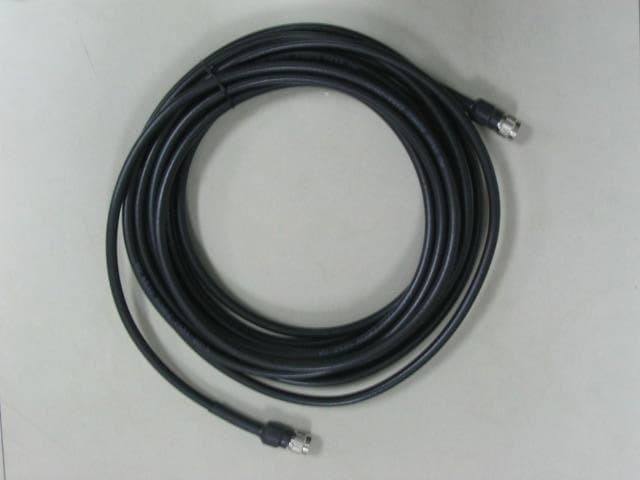
Click to zoom
Application Details
- Equipment Class
- DSS - Part 15 Spread Spectrum Transmitter
- Date of Grant
- Nov 08, 2005
- Application Purpose
- Original Equipment
- Date of Application
- Nov 08, 2005
- Equipment Note
- RFID R/W
- Frequency Range
- 902.20000000 - 927.80000000
- Country
- China
Documents & Files
Document Text
Text extracted from the exhibit documents filed with the FCC. Open a document above to read the original.
Users Manual
*** Caution *** Changes of modifications not expressly approved by the party responsible for compliance could void the user’s authority to operate the equipment XCRF-500 Reader Series Operation Manual Shenzhen Yuanwanggu Information Technology Co., Ltd. i Content Chapter 1: Introduction..........................................................1 1.1 System advantage.........................................................3 1.2 System capability characteristics..................................4 1.3 XCRF-500 reader series...............................................5 1.4 Other needed accessories..............................................6 Chapter 2: Installation............................................................7 2.1 Appearance of XCRF-500 reader series.......................7 2.2 Front and Upper Panel..................................................9 2.3 Back Panel..................................................................11 2.4 Installation steps.........................................................12 2.5 Connect external antenna............................................13 2.6 External antenna installation.......................................14 2.7 Connect serial port of PC............................................15 2.8 Connect to external AC power supply........................15 2.9 Reader Test..................................................................17 2.10 Adjust antenna position.............................................20 2.11 Test for reading the information of tag.....................20 2.12 Test for writing the information of tag......................20 Chapter 3: RF communication.............................................21 3.1 Signal interference......................................................21 3.2 Signal attenuation/reflection.......................................23 ii 3.3 Optimization of system performance..........................25 Chapter 4: Fault Diagnosis...................................................29 4.1 Faults that can be solved by user himself...................29 4.2 Contact customer service............................................32 1.Information of the Reader 2.Information of the Computer 4.3 Return of the Device...................................................34 Chapter 5: Performance Index.............................................37 Chapter 6: other explanation................................................39 6.1 Radio frequency (RF) radiation..................................39 6.2 Non promissory articles..............................................39 6.3 marketed method 1 Chapter 1: Introduction The XCRF-500 reader series are electronic tag readers developed by Shenzhen Yuanwanggu Information Technology Co., Ltd. These readers are applicable to reading/writing XCTF-5000 tag series that satisfies NCITS256-1999 protocol and works within UHF frequency range, as well as compatibly reading AMTECH’s UHF tag used in vehicle identification. With its compatible electronic tags, XCRF-500 reader series could be widely deployed in the areas like custom vehicle automatic identification, urban vehicle automatic identification management, highway non-stop toll, etc. XCRF-600 reader can only read the tags that meet the proposal of EM4223. XCRF-600 reader needs only to send RF power to tags, one tag will send its ID information. XCRF-600 reader can be widely deployed in the doorway management, etc. XCRF-500 reader series includes 4 reader models: XCRF-500W, XCRF-501W, XCRF-502W and XCRF-504W. XCRF-500W is single-ported reader where only antenna 1 can be connected with external antenna. XCRF-501W is antenna-built-in reader, XCRF-502W is dual-ported reader, 2 both antenna 1 and antenna 2 of which can be connected with external antenna. XCRF-504W is four-ported reader, antenna 1, antenna 2, antenna 3 and antenna 4 of which can be connected with external antenna. In the case that the reader you ordered is multi-ported, it is necessary to connect the unused antenna ports to 50/20W dummy load in order to protect the reader. 3 1.1 System Advantage From the point of data collection, radio frequency identification system completely resembles bar code system. In the course of data collection, bar code system adopts one-way communication, i.e., bar code sensor (reader) reads information from bar code in non-touch way. During such information flowing, bar code is totally in a passive and subordinate position and the communication is one-way, i.e., information is transmitted to bar code sensor from bar code tag. The shortcoming of bar code system is that, if damaged, polluted, damped or located inside an article, the bar code couldn’t acquire data because the reading range of sensor is too short. Data collection system composed of XCRF-500 reader series and their compatible electronic tags, fundamentally overcomes the above shortcoming of bar code system. The communication between reader and tag is two-way, in which the tag makes 4 relevant response to reader’s demand. With two-way communication, system could realize the function of reading multiple tags within reading area. Matched with appropriate antenna, the reading range of XCRF-500 reader series could be over 7 meters. 1.2 System Capability Characteristics ̄ Ability to read part of or all the data information of a single tag; ̄ Ability to read part of or all the data information of multiple tags under the circumstance of no unpacking and ordering; ̄ Ability to screen specific electronic tag according to the user-defined rules; The super inquiry protocol followed by reader and electronic tag enables reader to unerringly identify every electronic tag within reading area and read each tag only once. The unique protocol between reader and electronic tag decides that when multiple tags are read, every tag spends the same reading time, independent of tag quantity within reading area (regarding XCTF-5000 electronic tag). 5 1.3 XCRF-500 reader series XCRF-500 reader series a…
Text truncated - open the document above for the full version.
Block Diagram
1 OF 1 Block Diagram 1. System Module Block Diagram System Module Block Diagram 2. Radio Frequency Module Block Diagram Radio Frequency Module Block Diagram 2 OF 2 3. Base Band Module Block Diagram Base Band Module Block Diagram 4. Power Module Block Diagram Power Module Block Diagram Designer chenxiaohua date 07/19/2005 Principle Block Diagram Auditor wenyiqing date 70/30/2005
Cover Letter(s)
TIMCO 849 NW State Road 45 FCC Approvals Newberry, Florida 32669 Industry Canada Approvals http://www.timcoengr.com Notified Body for Europe 888.472.2424 F 352.472.2030 email: [email protected] 11/08/2005 MR. JIMMY ZHANG SHENZHEN HUATONGWEI INTERNATIONAL INSPECTION CO., LTD. 86-755-26715686 86-755-26748089 [email protected]; [email protected] SUBJECT: SHENZHEN YUANWANGGU INFORMATION TECHNOLOGY CO., LTD. - FCC ID: TQ4 REFERENCE: JOB 2200CC5 Dear MR. ZHANG: This application is on hold until these questions are resolved. Thank you for your reply and supporting documents. However, based upon our review of this application we have additional questions: 1. 2. 3. For your info - Please note that the FCC requires that we list the required separation distance on the Grant of Equipment Authorization. 4. Sincerely, Bruno Clavier
External Photos
Top View of EUT Bottom View of EUT Front View of EUT Back View of EUT Left View of EUT Right View of EUT Cable of System Antenna of System
ID Label/Location Info
Model Name: XCRF-500 Made in China FCC ID: TQ4YWGIT-R5678900 This device complies with part 15 of the FCC Rules. Operation is subject to the following two conditions: (1) This device may not cause harmful interference, and (2) this device must accept any interference received, including interference that may cause undesired operation.
ID Label/Location Info
Model Name: XCRF-500 Made in China FCC ID: TQ4YWGIT-R5678900 This device complies with part 15 of the FCC Rules. Operation is subject to the following two conditions: (1) This device may not cause harmful interference, and (2) this device must accept any interference received, including interference that may cause undesired operation.
Internal Photos
Internal of EUT-1 Internal of EUT-2 Internal of EUT-3 Internal of EUT-4 Internal of EUT-5 Internal of EUT-6 Internal of EUT-7 Internal of EUT-8 Internal of EUT-9 Internal of EUT-10 Internal of EUT-11
Operational Description
System Description 1.System Structure Diagram Diagram1: System Structure diagram The system consists of radio frequency module, Baseband module, power module, data interface and LED display interface. Under the control of Baseband module radio frequency module transmits the modulated carrier signal with varying frequency and power. The antenna transmits the signal to a certain area within which the tags receive the signal and then feedback its signal. After going into radio frequency module the feedback signal will be demodulated to form Baseband signal. . Baseband module performs decoding the tag signal and communicating with PC, and power module provides all the direct voltage . 2Radio Frequency Structure Diagram Phase Lock Looper Front Amplifier Six ports coupling Network End Amplifier End Amplifier Detector Power Front Amplifier Base_band Module Comparator Antenna Power Control ASK Signal Diagram2 radio frequency module diagram The radio frequency module consists of transmitting and receiving parts controlled by Baseband circuit. The Phase Lock Looper generates carrier with frequency range from 902MHz~928MHz, which could be amplified by the Front Amplifier and End Amplifier and then emitted by the antenna that returns tag’s signal via six ports coupling network to the detector, where the signal are detected and amplified to output to the Baseband circuit. 3Baseband Structure Diagram FPGA APA075 MCU MCF5272 LED Interface Power Data interface +I/O interface Radio Frequency Module PC or Switcher Diagram 3 Baseband module diagram 4Radio Frequency Module The radio frequency module consists of transmitting and receiving part. 2 z Transmitting Part The transmitting part is as below according to the RF signal flow. Temperature-compensated oscillator(12.8MHz) PLL915A phase lock looper RF2302 power front-amplifierend-amplifier(power adjustable) microwave switcher(Maximum output power: 30dBm). z Receiving part The receiving part is as below according to the returned(feedback) signal flow. six-ports coupling networkfront difference amplifier end amplifier comparator output. (Output double-channel digital signal). 5Baseband Module The Baseband module consists of coding/decoding and control parts, which respectively are FPGA(APA075) and IP2022 MCU. The coding/decoding part employs built-in-FLASH FPGA modeled APA075 produced by Actal Company. The device performs coding/decoding for tag and controlling the transmitting circuit. The control part employs IP2022 produced by Ubicom Company. With 19200bps serial interface and 10Mbps Ethernet network interface, IP2022 performs order analyzing, data uploading, and data storage, etc. 3
Schematics
1 2 3 4 5 6 78 ABCD 8 7 6 5 4 3 2 1 D CBA 1 YWGIT chenxiaohua wenyiqing wenyiqing 1 XCRMF-600 READER YW5.948.073DL 2005-05-11 14:31 Time: page A3 V1.3 authorizeauditordesigner Basebend pcb:XCRMF-600-MAINV1.3.pcb TSS 1 TSCK 2 TSI 3 TSO 4 RA0 5 RA1 6 RA2 7 RA3 8 DVDD 9 DVSS 10 IOVSS 11 IOVDD 12 RB0 13 RB1 14 RB2 15 RB3 16 RB4 17 RB5 18 RB6 19 RB7 20 RC0 21 RC1 22 RC2 23 RC3 24 RC4 25 RC5 26 RC6 27 RC7 28 RD0 29 RD1 30 DVDD 31 DVSS 32 IOVSS 33 IOVDD 34 RD2 35 RD3 36 RD4 37 RD5 38 RD6 39 RD7 40 RE0 41 RE1 42 RE2 43 RE3 44 RE4 45 RE5 46 RE6 47 RE7 48 RF0 49 RF1 50 RF2 51 RF3 52 IOVDD 53 IOVSS 54 DVSS 55 DVDD 56 RF4 57 RF5 58 RF6 59 RF7 60 RG0 61 RG1 62 RG2 63 RG3 64 GVDD 65 RG4 66 RG5 67 RG6 68 RG7 69 AVDD 70 AVSS 71 DVDD 72 DVSS 73 RTCLK1 74 RTCLK2 75 XVDD 76 XVSS 77 OSC1 78 OSC2 79 RST 80 U2 IP2022 2.5V 2.5V 2.5V 2.5V 2.5V 2.5V 2.5V 3.3V 3.3V 3.3V GND GND GND GNDGND GND GND GNDGND ADDR0ADDR1ADDR2ADDR3 ADDR4 ADDR5 ADDR6 ADDR7 DATA0 DATA1 DATA2 DATA3 DATA4 DATA5 DATA6 DATA7 UART_RXUART_TXETH_TX+_150ETH_TX+_22ETH_TX-_22ETH_TX-_150MLED_ACTMLED_LINK ETH_RX+ ETH_RX- IP2022_TSOIP2022_TSIIP2022_TSCKIP2022_TSS RESET MCU_CLOCK 12345678 9 10 J3 RJ-45B R15 75 R16 75 R17 75 R18 75 NGND C101000pF/2KV 1 --- TX+2 --- TX-3 --- RX+6 --- RX-4 --- NC5 --- NC7 --- NC8 --- NC TX+TX-RX+ RX- C8 0.1uF C7 0.1uF R13 150 R10 22 R11 150 R12 22 R14100 10BASE-T 123678 91011141516 U7T16302DF C91000pF/2KV NGND NGND C1+ 1 V+ 2 C1- 3 C2+ 4 C2- 5 V- 6 T2out 7 R2in 8 R2out 9 T2in 10 T1in 11 R1out 12 R1in 13 T1out 14 GND 15 VCC 16 U10ADM202EARN C30 0.1uF C28 0.1uF C32 0.1uF C29 0.1uF 162738495 J4DB9 I2C_CLOCKI2C_DATA X1 1 X2 2 Vbat 3 GND 4 SDA 5 SCL 6 OUT 7 VCC 8 U4DS1307 X1 32.768kHZ 1 2 BATT1Battery 3.3V I2C_CLOCKI2C_DATA R7 10KR6 10K 5V GND GND 5V 5V I2C_CLOCKI2C_DATA 5V NC 1 VIN1 2 VIN1 3 MR1 4 MR2 5 EN 6 SEQ 7 GND 8 VIN2 9 VIN2 10 NC 11 VOUT2 12 VOUT2 13 VSENSE2 14 RESET 15 PG1 16 VSENSE1 17 VOUT1 18 VOUT1 19 NC 20 U6TPS70158 NC 1 GND 2 CLK 3 VCC 4 U924MHz A0 1 A1 2 NC 3 GND 4 SDA 5 SCL 6 WP 7 VCC 8 U5AT24C512 3.3V GND MCU_CLOCK C30.1uF 5V5V C40.1uF C510uF/16V R8 240K R9240K C610uF/16V RESET 2.5V3.3V C110.1uF C140.1uF C170.1uF 3.3VGND C120.1uF C150.1uF C180.1uF C130.1uF C160.1uF C190.1uF GND2.5V C360.1uF C410.1uF 2.5VGND C370.1uF C420.1uF C380.1uF C430.1uF GND C390.1uF C440.1uF C400.1uF C450.1uF 3.3V ETH_RX+ETH_RX-ETH_TX-_150ETH_TX-_22ETH_TX+_22ETH_TX+_150GNDUART_RXUART_TX C3147uF/16V C330.1uF IO 控制驱动及接口 通讯接口 FPGA 退耦电容 FP G A 编程接口 IP2022 退耦电容 电源模块 LED 驱动及接 口 RTC_INT GND 1 I/O 2 I/O 3 I/O 4 I/O 5 I/O 6 I/O 7 I/O 8 GND 9 I/O / GLMX1 10 I/O / GL1 11 AGND 12 NPECL1 13 AVDD 14 PPECL1 / input 15 I/O / GL2 16 VDD 17 I/O 18 I/O 19 I/O 20 I/O 21 I/O 22 I/O 23 I/O 24 GND 25 VDDP 26 I/O 27 I/O 28 I/O 29 I/O 30 I/O 31 I/O 32 I/O 33 I/O 34 I/O 35 I/O 36 VDD 37 GND 38 VDDP 39 GND 40 I/O 41 I/O 42 I/O 43 I/O 44 I/O 45 I/O 46 TCK 47 TDI 48 TMS 49 VDDP 50 GND 51 VPP 52 VPN 53 TDO 54 TRST 55 RCK 56 I/O 57 I/O 58 I/O 59 I/O / GL3 60 PPECL2 / Input 61 AVDD 62 NPECL2 63 AGND 64 I/O / GL4 65 I/O / GLMX2 66 GND 67 VDD 68 I/O 69 I/O 70 I/O 71 I/O 72 I/O 73 I/O 74 GND 75 VDDP 76 I/O 77 I/O 78 I/O 79 I/O 80 I/O 81 I/O 82 I/O 83 I/O 84 I/O 85 GND 86 VDDP 87 GND 88 VDD 89 I/O 90 I/O 91 I/O 92 I/O 93 I/O 94 I/O 95 I/O 96 I/O 97 I/O 98 I/O 99 VDDP 100 U11 APA075 GND GND GND 2.5V 3.3V 3.3V 3.3V ADDR0ADDR1ADDR2ADDR3 ADDR4 ADDR5 ADDR6 ADDR7 DATA0 DATA1 DATA2 DATA3 DATA4 DATA5 DATA6 DATA7 3.3V GND FPGA_TCK FPGA_TDI FPGA_TMS FPGA_VPPFPGA_VPNFPGA_TDOFPGA_TRSTFPGA_RCK GND GND GND 3.3V 2.5V 3.3V GNDGNDGND GNDGND2.5V2.5V 2.5V2.5V FPGA_TEST0FPGA_TEST1FPGA_TEST2FPGA_TEST3 FPGA_CLOCK FPGA_INT MCU_RDMCU_WR MCU_WR MCU_RD FPGA_INTRTC_INTMCU_INPUT0MCU_INPUT1MCU_INPUT2MCU_INPUT3MCU_OUTPUT0MCU_OUTPUT1MCU_OUTPUT2MCU_OUTPUT3 NC 1 GND 2 CLK 3 VCC 4 U824MHz 3.3V GND FPGA_CLOCK 5V GND GND GND IP2022_TSORS232_RXDRS232_TXDIP2022_TSSIP2022_TSCKIP2022_TSI5V 12345678910 J6CON10 IO_INPUT1IO_INPUT2IO_INPUT3IO_INPUT0IO_OUTPUT1IO_OUTPUT2IO_OUTPUT3IO_OUTPUT0 OE1 1 1A0 2 1A1 4 1A2 6 1A3 8 GND 10 VCC 20 2Y0 3 2Y1 5 2Y2 7 2Y3 9 OE2 19 2A0 17 2A1 15 2A2 13 2A3 11 1Y0 18 1Y1 16 1Y2 14 1Y3 12 U1374HCT244 C260.1uF C27 10uF/16V 5V 5V GND GND GND 5V MCU_OUTPUT0MCU_OUTPUT1MCU_OUTPUT2MCU_OUTPUT3MCU_INPUT0MCU_INPUT1MCU_INPUT2MCU_INPUT3 OE1 1 1A0 2 1A1 4 1A2 6 1A3 8 GND 10 VCC 20 2Y0 3 2Y1 5 2Y2 7 2Y3 9 OE2 19 2A0 17 2A1 15 2A2 13 2A3 11 1Y0 18 1Y1 16 1Y2 14 1Y3 12 U1474HCT244 12345678910 J7CON10 FLED_DY1FLED_DY2FLED_RF1FLED_RF2 FLED_JSFLED_ERR LED_JSLED_ERRLED_LINKLED_ACT LED_DY1LED_DY2LED_RF1LED_RF2LED_JSLED_ERRLED_LINKLED_ACT C340.1uF C35 10uF/16V GND GND GND GND5V 5V FLED_LINKFLED_ACT 5VGND C2110uF/16V C25 0.1uF C2010uF/16V C22 0.1uF C2410uF/16V C23 0.1uF 3.3VGND 5V 2.5VGND 123456789 101112 J5CON12 FPGA_TCKFPGA_TDIFPGA_TMSFPGA_VPPFPGA_VPNFPGA_TDOFPGA_TRSTFPGA_RCK GNDGND 2.5V3.3V 2.5VGNDGNDGND3.3V3.3V LD5RED R35510 FF_LINK MPLL_RESETMAD_RESETMDC_RESETMCU_BEEPMRF_POWER MPLL_RESET MAD_RESET MDC_RESET MLED_LINK MLED_ACT FAD_CS FAD_SDI FAD_CLK F_PDATA F_PCLK F_PEN F_AIN F_AOUT0 F_AOUT1 F_ANT0 F_ANT1 FLED_DY1FLED_DY2FLED_RF1FLED_RF2FLED_JSFLED_ERRFLED_LINKFLED_ACT GND 灯板 接 口 LD4 RED R34510 3.3V LD3RED R33510 2.5V LD2RED 5V LD6RED R36510 FF_ACT R321.0K FF_ACTFF_LINK IN 1 GND 2 OUT 3 U3 MIC29150 RF_VCC 5V VIN 1 VOUT 2 GND 3 FB 4 EN 5 U1LM2576T-ADJ C1100uF/16V A 1 K 2 D1IN5822 L1100uH/3A R22.0KR16.8K RF_VCC 12 J2CON2 R29 20KR30 20K3.3V FPGA_TDOFPGA_TCK C201220uF/10V C202220uF/10V C203220uF/10V C204220uF/10V RF_VCC C540.1uF C550.1uF 2.5VGND C560.1uF 2.5VGND C200 220uF/10V RF_VCC RF_VCC C301220uF/10V C302220uF/10V L300BLM31PG391SN1L 5V RF_5V GND L301BLM31PG391SN1L 12 C303220uF/10V GND IF_AOUT0IF_AOUT1 RF R402.2KR422.2K R413.3KR433.3K F_AOUT0F_AOUT1 C520.1uF C53 10uF/16V 5VGND MCU_BEEP RF 驱动 RF_PLL_DATARF_PLL_CLKRF_PLL_EN OE1 1 1A0 2 1A1 4 1A2 6 1A3 8 GND 10 VCC 20 2Y0 3 2Y1 5 2Y2 7 2Y3 9 OE2 19 2A0 17 2A1 15 2A2 13 2A3 11 1Y0 18 1Y1 16 1Y2 14 1Y3 12 U15 74HCT244 RF_ASK_IN F_PDATAF_PCLKF_PENF_AIN GND5V GND GND MRF_POWERFAD_CLKFAD_CSFAD_SDI OE1 1 1A0 2 1A1 4 1A2 6 1A3 8 GND 10 VCC 20 2Y0 3 2Y1 5 2Y2 7 2Y3 …
Text truncated - open the document above for the full version.
Test Report
Shenzhen Huatongwei International Inspection Co., Ltd REPORT NO: TR05090017 FCC ID: TQ4YWGIT-R5678900 DATE: 10/24/2005 Page 1 Rev. 00 ELECTROMAGNETIC EMISSIONS COMPLIANCE REPORT INTENTIONAL RADIATOR CERTIFICATION TO FCC PART 15 SUBPART C REQUIREMENT OF RFID R/W FCC ID:TQ4YWGIT-R5678900 MODEL No.: XCRF-500 XCRF-600 BRAND NAME: N/A REPORT NO: TR05090017 ISSUE DATE: October 24, 2005 Prepared for SHENZHEN YUANWANGGU INFORMATION TECHNOLOGY CO., LTD. 3/F. NO. T2-B. HIGH-TECH INDUSTRIAL PARK SOUTH, SHENZHEN Prepared by SHENZHEN HUATONGWEI INTERNATIONAL INSPECTION CO., LTD d.b.a. SHENZHEN HUATONGWEI INTERNATIONAL INSPECTION CO., LTD HUATONGWEI BUILDING, KEJI RD. 12 S., HIGH-TECH PARK, NANSHAN DISTRICT, SHENZHEN, GUANGDONG , P.R.CHINA TEL: 86-755-26748099 FAX: 86-755-26748089 Shenzhen Huatongwei International Inspection Co., Ltd REPORT NO: TR05090017 FCC ID: TQ4YWGIT-R5678900 DATE: 10/24/2005 Page 2 Rev. 00 VERIFICATION OF COMPLIANCE Applicant: SHENZHEN YUANWANGGU INFORMATION TECHNOLOGY CO., LT D . 3/F. NO. T2-B. HIGH-TECH INDUSTRIAL PARK SOUTH, SHENZHEN Manufacturer SHENZHEN YUANWANGGU INFORMATION TECHNOLOGY CO., LT D . 3/F. NO. T2-B. HIGH-TECH INDUSTRIAL PARK SOUTH, SHENZHEN Product Description: RFID R/W Brand Name: N/A Model Number: XCRF-500; XCRF-600 Serial Number: N/A File Number: SQE05090017 Date of Test: September 28, 2005 ~ October 13, 2005 We hereby certify that: The above equipment was tested by SHENZHEN HUA TONG WEI INTERNATIONAL INSPECTION CO., LTD. The test data, data evaluation, test procedures, and equipment configurations shown in this report were made in accordance with the procedures given in ANSI C63.4 (2003) and the energy emitted by the sample EUT tested as described in this report is in compliance with radiated emission limits of FCC Rules Part 15.247. The test results of this report relate only to the tested sample identified in this report. Reviewed By Jimmy Li / Technical Manager SHENZHEN HUA TONG WEI INTERNATIONAL INSPECTION CO., LTD Shenzhen Huatongwei International Inspection Co., Ltd REPORT NO: TR05090017 FCC ID: TQ4YWGIT-R5678900 DATE: 10/24/2005 Page 3 Rev. 00 Table of Contents 1. GENERAL INFORMATION................................................................................................ 4 1.1 Product Description ............................................................................................................................ 4 1.2 Related Submittal(s) / Grant (s)......................................................................................................... 4 1.3 Test Methodology ................................................................................................................................ 4 1.4 Test Facility ......................................................................................................................................... 4 2. SYSTEM TEST CONFIGURATION .................................................................................. 5 2.1 Configuration of Tested System......................................................................................................... 5 3. Summary of Test Result.........................................................................................................7 4. DESCRIPTION OF TEST MODES..................................................................................... 7 5. PARAMETERS FOR GAME PAD ...................................................................................... 8 5.1 Conduction Emission .......................................................................................................................... 8 5.2 Hopping Channels............................................................................................................................. 10 5.3 Channel Separation........................................................................................................................... 13 5.4 20 dB Bandwidth ............................................................................................................................... 15 5.5 Operation Frequency ........................................................................................................................ 19 5.6 Peak Output Power ........................................................................................................................... 5.7 Spurious Emission at Transmitting Mode ...................................................................................... 5.8 Band Edge .......................................................................................................................................... 25 5.9 Spurious Emission at Receiving Mode ............................................................................................28 5.10 Dwell Time ......................................................................................................................................... 30 APPENDIX 1 PHOTOGRAPHS OF SET UP..............................................................................33 APPENDIX 2 PHOTOGRAPHS OF EUT...................................................................................35 Shenzhen Huatongwei International Inspection Co., Ltd REPORT NO: TR05090017 FCC ID: TQ4YWGIT-R5678900 DATE: 10/24/2005 Page 4 Rev. 00 1 GENERAL INFORMATION 1.1 Product Description The EUT is an short range, lower power, RFID reader and writer designed as an “ Input Device”. It is designed by way of utilizing the FHSS technology to achieve the system operation. A major technical descriptions of EUT is described as following: A). Operation Frequency: From 903.0 MHz – 927.5 MHz for XCRF-500 total 50 channels with 500 KHz intervals, the maximum selectable hopping frequencies is 20 channels at one time. ( 903.0 MHz, 903.5 MHz,......, 927.0 MHz, 927.5 MHz ) From 902.2 MHz – 927.8 MHz for XCRF-600 total 129 channels with 200 KHz intervals, the maximum selectable hopping frequencies is 60 channels at one time. ( 902…
Text truncated - open the document above for the full version.
Test Setup Photos
Conducted Emission Setup Photos Radiated Emission Setup Photos
Contact Information
Applicant
Luke Xie(Certification Engineer)
Test Firm
Shenzhen Huatongwei International Insp. Co., LtdMoffy Yu
Technical Specifications
| # | Rule Parts | Frequency Range | Power Output |
|---|---|---|---|
| 1 | 15C | 902.2 MHz - 927.8 MHz | 901.00 mW |
Other Applications from Invengo Information Technology Co., Ltd.

TQ4-XC-RF700
Sep 28, 2024Reader
Equipment Class
DSS - Part 15 Spread Spectrum Transmitter
TQ4-XC-RF862
Sep 25, 2024Reader
Equipment Class
DSS - Part 15 Spread Spectrum TransmitterTQ4-XC-RF868
Jul 28, 2022Reader
Equipment Class
DTS - Digital Transmission System
TQ4-XC2907A
Apr 29, 2021Portable reader
Equipment Class
DSS - Part 15 Spread Spectrum Transmitter
TQ4-XC-RF855
Jan 07, 2020reader-writer
Equipment Class
DXX - Part 15 Low Power Communication Device Transmitter