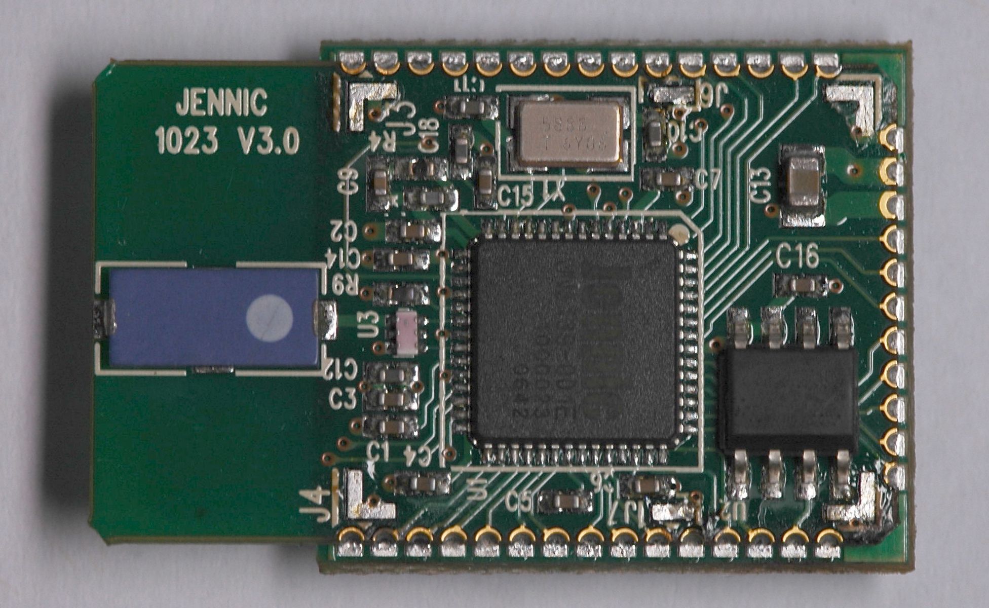
TYOJN5139M0IEEE 802.15.4 Wireless Microcontroller
NXP Laboratories UK Ltd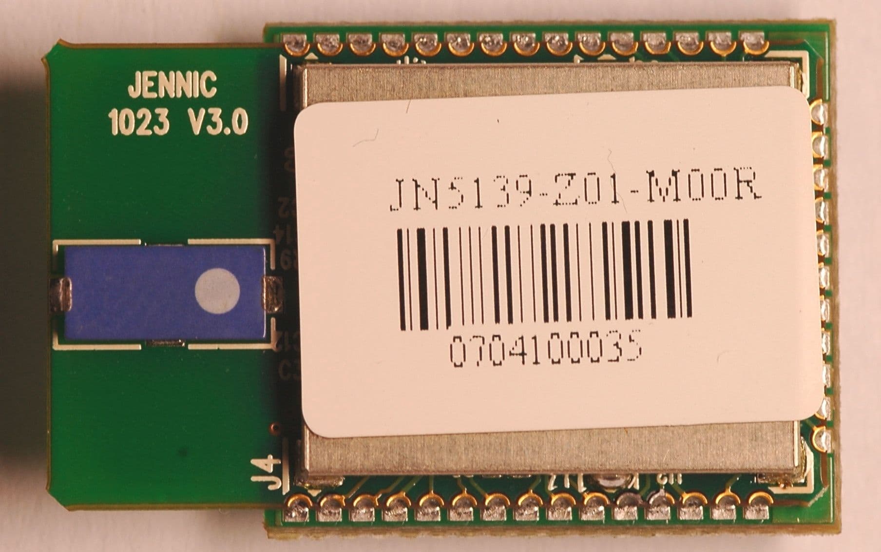
Click to zoom
Application Details
- Equipment Class
- DTS - Digital Transmission System
- Date of Grant
- Mar 27, 2007
- Application Purpose
- Original Equipment
- Date of Application
- Mar 27, 2007
- Equipment Note
- IEEE 802.15.4 Wireless Microcontroller
- Frequency Range
- 2400.00000000 - 2483.50000000
- Company
- NXP Laboratories UK Ltd
- Country
- United Kingdom
Documents & Files
Document Text
Text extracted from the exhibit documents filed with the FCC. Open a document above to read the original.
Users Manual
Advanced Data Sheet – JN513x IEEE802.15.4 and ZigBee Wireless Microcontrollers i JN-DS-JN513x v1.1 © Jennic 2007 Advanced Features: Transceiver • 2.4GHz IEEE802.15.4 compliant • 128-bit AES security processor • MAC accelerator with packet formatting, CRCs, address check, auto-acks, timers • Integrated power management and sleep oscillator for low power • On-chip power regulation for 2.2V to 3.6V battery operation • Deep sleep current <0.4μA • Sleep current with active beacon timer <1.5μA • Needs minimum of external components (< US$1 cost) • Rx current 39mA • Tx current 39mA • Receiver sensitivity -97dBm • Transmit power +3dBm Features: Microcontroller • 32-bit RISC processor sustains 32MIPs with low power • 192kB ROM stores system code, including protocol stack • 8kB, 16kB, 32kB or 96kB RAM stores system data and optionally bootloaded program code • 48-byte OTP eFuse, stores MAC ID on-chip, offers AES based code encryption feature • 4-input 12-bit ADC, 2 11-bit DACs, 2 comparators • 2 Application timer/counters, 3 system timers • 2 UARTs (one for debug) • SPI port with 5 selects • 2-wire serial interface • Up to 21 GPIO Industrial temperature range (-40°C to +85°C) 8x8mm 56-lead QFN – pin compatible with JN5121 Lead-free and RoHS compliant Overview The JN513x are a family of low power, low cost wireless microcontrollers suitable for IEEE802.15.4 and ZigBee applications. Each device integrates a 32-bit RISC processor, with a fully compliant 2.4GHz IEEE802.15.4 transceiver, 192kB of ROM, a selection of RAM sizes from 8kB to 96kB, and a rich mixture of analogue and digital peripherals. The cost sensitive ROM/RAM architecture supports the storage of system software, including protocol stacks, routing tables and application code/data. Each device has hardware MAC and AES encryption accelerators, power saving and timed sleep modes, and mechanisms for security key and program code encryption. These features all make for a highly efficient, low power, single chip wireless microcontroller for battery-powered applications. Block Diagram Benefits • Single chip integrates transceiver and microcontroller for wireless sensor networks • Cost sensitive ROM/RAM architecture, meets needs for volume application • System BOM is low in component count and cost • Hardware MAC ensures low power consumption and low processor overhead • Extensive user peripherals • Pin compatible wit h JN5121 for easy migration Applications • Robust and secure low power wireless applications • Wireless sensor networks, particularly IEEE802.15.4 and ZigBee systems • Home and commercial building automation • Remote Control • Toys and gaming peripherals • Industrial systems • Telemetry and utilities (e.g. AMR) Optional 32-bit RISC CPU Timers UARTs 12-bit ADC, comparators 11-bit DACs, temp sensor 2-wire serial SPI RAM 8kB - 96kB 128-bit AES Encryption Accelerator 2.4GHz Radio ROM 192kB Power Management XTAL O-QPSK Modem IEEE802.15.4 MAC Accelerator Bootloader Flash 48-byte OTP eFuse Jennic JennicJennic Jennic ii JN-DS-JN513x v1.1 © Jennic 2007 Advanced Contents 1 Introduction 1 1.1 Wireless Microcontroller 1 1.2 Wireless Transceiver 1 1.3 RISC CPU and Memory 1 1.4 Peripherals 2 1.5 Block Diagram 3 2 Pin Configurations 4 2.1 Pin Assignment 5 2.2 Pin Descriptions 6 2.2.1 Power Supplies 6 2.2.2 Reset 6 2.2.3 16MHz System Clock 6 2.2.4 Radio 6 2.2.5 Analogue Peripherals 6 2.2.6 Digital Input/Output 7 3 CPU 8 4 Memory Organisation 9 4.1 ROM 10 4.2 RAM 10 4.3 OTP eFuse Memory 10 4.4 External Memory 11 4.4.1 Secure External Memory Encryption 11 4.5 Peripherals 11 4.6 Unused Memory Addresses 11 5 System Clocks 12 5.1 16MHz Oscillator 12 5.2 32kHz Oscillator 12 6 Reset 13 6.1 Power-on Reset 13 6.2 External Reset 13 6.3 Software Reset 14 6.4 Brown-out Detect 14 7 Interrupt System 15 7.1 System Calls 15 7.2 Processor Exceptions 15 7.2.1 Bus Error 15 7.2.2 Alignment 15 7.2.3 Illegal Instruction 15 7.3 Hardware Interrupts 16 8 Wireless Transceiver 17 8.1 Radio 17 8.1.1 Radio External components 18 8.1.2 Antenna Diversity 18 8.2 Modem 19 Jennic JennicJennic Jennic © Jennic 2007 JN-DS-JN513x v1.1 iii 8.3 Baseband Processor 20 8.3.1 Transmit 20 8.3.2 Reception 20 8.3.3 Auto Acknowledge 21 8.3.4 Beacon Generation 21 8.3.5 Security 21 8.4 Security Coprocessor 21 9 Digital Input/Output 22 10 Serial Peripheral Interface 23 10.1 Programming Example 25 11 Intelligent Peripheral Interface 27 11.1 Data Transfer Format 27 11.2 JN513x Initiated Data Transfer 28 11.3 Remote Processor Initiated Data Transfer 28 12 Timers 29 12.1 Peripheral Timer / Counters 29 12.1.1 Pulse Width Modulation Mode 30 12.1.2 Capture Mode 30 12.1.3 Counter / Timer Mode 31 12.1.4 Delta-Sigma Mode 31 12.1.5 Timer / Counter Application 32 12.2 Tick Timer 33 12.3 Wakeup Timers 34 12.3.1 RC Oscillator Calibration 34 12.3.2 External 32kHz Clock Source 35 13 Serial Communications 36 13.1 Interrupts 37 13.2 UART Application 37 13.3 Programming Example 38 14 Two-Wire Serial interface 39 14.1 Connecting Devices 40 14.2 Multi-Master Operation 40 14.3 Clock Stretching 41 14.4 Programming Example 41 15 Analogue Peripherals 43 15.1 Analogue to Digital Converter 44 15.1.1 Operation 44 15.1.2 Supply Monitor 44 15.1.3 Temperature Sensor 45 15.1.4 Programming Example 45 15.2 Digital to Analogue Converter 45 15.2.1 Operation 45 15.2.2 Programming Example 46 15.3 Comparators 46 16 Power Management and Sleep Modes 48 Jennic JennicJennic Jennic iv JN-DS-JN513x v1.1 © Jennic 2007 Advanced 16.1 Operating Modes 48 16.1.1 Power Domains 48 16.2 Active Processing Mode 48 16.2.1 CPU Doze 48 16.3 Sleep Mode 48 16.3.1 Wakeup Timer Event 49 16.3.2 DIO Event 49 16.3.3 Comparator Event 49 16.4 Deep Sleep Mode 49 17 Electrical Characteristics 50 17.1 Maximum ratings 50 17.2 DC Electrical Characteristics 50 17.2.1 Operating Conditions 50 17.2.2 DC Current Consumption 51 17.2.3 I/O Characteristics 52 17.3 AC Characteristics 52 17.3.1 Reset 52 17.3.2 Brown-out Detect 53 17.3.3 SPI Timing 54 17.3.4 Two-wire serial inter…
Text truncated - open the document above for the full version.
Users Manual
Advanced Data Sheet – JN5139-xxx-Myy IEEE802.15.4/ZigBee Module Family Preliminary - JN-DS-JN5139-xxx-Myy v1.1 © Jennic 2007 Advanced Information Features: Module • 2.4GHz IEEE802.15.4 & ZigBee compliant • 2.7-3.6V operation • Sleep current (with active sleep timer) 2μA • JN5139-xxx-M00/01/03 > 1km range M00 has on board antenna M01 has SMA connector M03 has uFl connector o Receiver sensitivity -97dBm o TX power +3dBm o TX current < 39mA o RX current < 39mA o 18x30mm • JN5139-xxx-M02/04 > 4km range M02 has SMA connector M04 has uFl connector o Receiver sensitivity -100dBm o 19dBm TX power o TX current < 120mA o RX current < 45mA o 18x40.5mm Features: Microcontroller • 16MHz 32-bit RISC CPU • 96kB RAM, 192kB ROM • 4-input 12-bit ADC, 2 11-bit DACs, 2 comparators, temperature sensor • 2 Application timer/counters, 3 system timers • 2 UARTs (one for in-system debug) • SPI port with 5 selects • 2-wire serial interface • 21 GPIO • Evaluation kits available with full, unlimited, Software Development Kit Industrial temperature range (-20°C to +70°C) Lead-free and RoHS compliant Overview The JN5139-xxx-Myy family is a range of surface mount modules that enable users to implement IEEE802.15.4 or ZigBee compliant systems with minimum time to market and at the lowest cost. They remove the need for expensive and lengthy development of custom RF board designs and test suites. The modules use Jennic’s JN5139 wireless microcontroller to provide a comprehensive solution with high radio performance and all RF components included. All that is required to develop and manufacture wireless control or sensing products is to connect a power supply and peripherals such as switches, actuators and sensors, considerably simplifying product development. Three basic hardware module variants are available: JN5139-xxx-M00 with an integrated antenna, JN5139-xxx-M01/M03 with an antenna connector and JN5139- xxx-M02/M04 with a power amplifier and LNA for extended range. Each variant can be provided pre-programmed with a ZigBee network stack (JN5139-Z01-Myy). Module Block Diagram Benefits • Microminiature module solutions • Ready to use in products • Minimises product development time • No RF test required for systems • Compliant with FCC part 15 rules, ETSI ETS 300-328 and Japan ARIB STD-T66 • Production volumes supplied pre-programmed with application software Applications • Robust and secure low power wireless applications • Wireless sensor networks, particularly IEEE802.15.4 / ZigBee systems • Home and commercial building automation • Home networks • Toys and gaming peripherals • Industrial systems • Telemetry and utilities (e.g. AMR) Ti mers UARTs 12-bit ADC, comparators 11- bi t DACs, temp sensor 2-wire serial SPI RAM 96kB 128-bit AES Encr ypt i on Accelerator 2. 4GHz Radi o ROM 192kB RI SC CPU Power Management XTAL O- QPSK Modem IEEE802.15.4 MAC Accel erator 128kB Serial Fl ash Memory JN5139 chip Power Bal un Connector Bal un Cerami c Antenna Bal unConnectorPA / LNA Exter nal Ant enna M00 Option M01/03 Option M02/04 Option Jennic ii Preliminary - JN-DS-JN5139-xxx-Myy v1.1 © Jennic 2007 Contents 1. Introduction 3 1.1. Variants 3 1.2. Regulatory Approvals 3 2. Specifications 4 3. Product Development 5 3.1. JN5139 Single Chip Wireless Microcontroller 5 4. Pin Configurations 6 4.1. Pin Assignment 7 4.2. Pin Descriptions 8 4.3. Power Supplies 8 4.4. SPI Memory Connections 8 5. Electrical Characteristics 9 5.1. Maximum Ratings 9 5.2. Operating Conditions 9 Appendix A Additional Information 10 A.1 Outline Drawing 10 A.2 Module PCB Footprint 15 A.3 Ordering Information 16 A.4 Tape and Reel Information: 17 A.4.1 Tape Orientation and dimensions 17 A.4.2 Cover tape details 17 A.4.3 Leader and Trailer 18 A.4.4 Reel Dimensions: 18 A.5 Related Documents 19 A.6 Federal Communication Commission Interference Statement 19 A.7 RoHS Compliance 20 A.8 Status Information 20 A.9 Disclaimers 21 A.10 Version Control 21 A.11 Contact Details 22 Jennic © Jennic 2007 Preliminary - JN-DS-JN5139-xxx-Myy v1.1 3 1. Introduction The JN5139-xxx-Myy module family provides designers with a ready made component which allows IEEE802.15.4 [1] wireless applications, including ZigBee, to be quickly and easily included in product designs. The modules integrate all of the RF components, removing the need to perform expensive RF design and test. Products can be designed by simply connecting sensors and switches to the module IO pins. The modules use Jennic’s single chip IEEE802.15.4 Wireless Microcontroller, allowing designers to make use of the extensive chip development support material. Hence, this range of modules allows designers to bring wireless applications to market in the minimum time with significantly reduced development effort and cost. Three basic module hardware variants are available: JN5139-xxx-M00 (standard module with on board ceramic antenna), JN5139-xxx-M01 (standard module with SMA connector for use with external antennae) and JN5139-xxx- M02 (high RF power, improved sensitivity module for extended range applications). uFL connector variants are provided (-M03 standard power and –M04 high power) for FCC approved products and for applications where a small connector size is required. Each of these modules can be supplied with a range of protocol stacks, including a simple IEEE802.15.4 protocol for point to point and star applications and a ZigBee mesh networking stack. The variants available are described below. 1.1. Variants 1.2. Regulatory Approvals All module types have been tested against the requirements of European standard ETS 300 328 and a certificate of compliance to this standard is available on request. The High Power modules with M02 suffix are approved for use in Europe with reduced output power. They must not be used with PHY_PIB_ATTR_TX_POWER set above 3 See [4]. Additionally, modules with M00, M03 and M04 suffixes have received FCC “Modular Approvals”, in compliance with CFR 47 FCC part 15 regulations and in accordance to …
Text truncated - open the document above for the full version.
Block Diagram
RADIO BLOCK DIAGRAM The radio comprises a low-IF receive path and a direct up-conversion transmit path, which converge at the TX/RX switch. This switch includes the necessary matching components such that a 200Ω differential antenna may be directly connected without external components. Alternatively, a balun can be used for single ended antennas. The 16MHz crystal oscillator feeds a divider, which provides the frequency synthesiser with a reference frequency. The synthesiser contains programmable feedback dividers, phase detector, charge pump and internal Voltage Controlled Oscillator (VCO). The VCO has no external components, and includes calibration circuitry to compensate for differences in internal component values due to process and temperature variations. The VCO is controlled by a Phase Lock Loop (PLL) that has a loop filter comprising 3 external components. A programmable charge pump is also used to tune the loop characteristic. Finally, quadrature (I and Q) local oscillator signals for the mixer drives are derived. The receiver chain starts with the low noise amplifier / mixer combination whose outputs are passed to the polyphase bandpass filter. This filter provides the channel definition as well as image frequency rejection. The signal is then passed to two variable gain amplifier blocks. The gain control for these stages, and the bandpass filter, is derived in the automatic gain control (AGC) block within the Modem. The signal is conditioned with the anti-alias low pass filter, before being converted to a digital signal with a flash ADC. In the transmit direction, the digital I and Q streams from the Modem are passed to I and Q quadrature DAC blocks which are buffered and low-pass filtered, before being applied to the modulator mixers. The summed 2.4 GHz signal is then passed to the RF Power Amplifier (PA), whose power control can be selected from one of six settings. The output of the PA drives the antenna via the RX/TX switch. 1600 MHz 1600 MHz 3MHz 1600 MHz
ID Label/Location Info
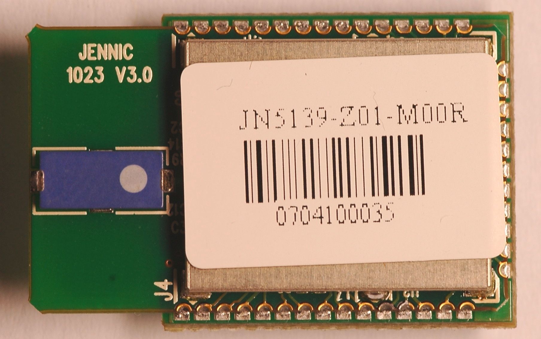
JN5139-XXX-M00 Module Labelling 1 Location: JN5139-000-M00 Subsequent to being granted an FCC-ID the following label will be used for JN5139- 000-M00. Product Identification Instructions Label line 1: FCC ID Number Label line 2: Part Name Label line 3: Barcode Label line 4: YYWWTNNNNN (see below) Identifier Description Format YY Year 06(example) WW Week 45(example) T Module type 0 NNNNN Serial Number Note, the R suffix on the part name indicates prototype. 1 JN5139_XXX_M00_FCC_label_1v0.doc revision 1.1 CF. FCCID: TYOJN5139M0 YYWWTNNNNN JN5139-000-M00R LABEL PLACED HERE. JN5139-Z01-M00 Subsequent to being granted an FCC-ID the following label will be used for JN5139- Z01-M00. Product Identification Instructions Label line 1: FCC ID Number Label line 2: Part Name Label line 3: Barcode Label line 4: YYWWTNNNNN (see below) Identifier Description Format YY Year 06(example) WW Week 45(example) T Module type 1 NNNNN Serial Number Note, the R suffix on the part name indicates prototype. FCCID: TYOJN5139M0 YYWWTNNNNN JN5139-Z01-M00R
Operational Description
RADIO BLOCK DIAGRAM The radio comprises a low-IF receive path and a direct up-conversion transmit path, which converge at the TX/RX switch. This switch includes the necessary matching components such that a 200Ω differential antenna may be directly connected without external components. Alternatively, a balun can be used for single ended antennas. The 16MHz crystal oscillator feeds a divider, which provides the frequency synthesiser with a reference frequency. The synthesiser contains programmable feedback dividers, phase detector, charge pump and internal Voltage Controlled Oscillator (VCO). The VCO has no external components, and includes calibration circuitry to compensate for differences in internal component values due to process and temperature variations. The VCO is controlled by a Phase Lock Loop (PLL) that has a loop filter comprising 3 external components. A programmable charge pump is also used to tune the loop characteristic. Finally, quadrature (I and Q) local oscillator signals for the mixer drives are derived. The receiver chain starts with the low noise amplifier / mixer combination whose outputs are passed to the polyphase bandpass filter. This filter provides the channel definition as well as image frequency rejection. The signal is then passed to two variable gain amplifier blocks. The gain control for these stages, and the bandpass filter, is derived in the automatic gain control (AGC) block within the Modem. The signal is conditioned with the anti-alias low pass filter, before being converted to a digital signal with a flash ADC. In the transmit direction, the digital I and Q streams from the Modem are passed to I and Q quadrature DAC blocks which are buffered and low-pass filtered, before being applied to the modulator mixers. The summed 2.4 GHz signal is then passed to the RF Power Amplifier (PA), whose power control can be selected from one of six settings. The output of the PA drives the antenna via the RX/TX switch. 1600 MHz 1600 MHz 3MHz 1600 MHz
Parts List/Tune Up Info
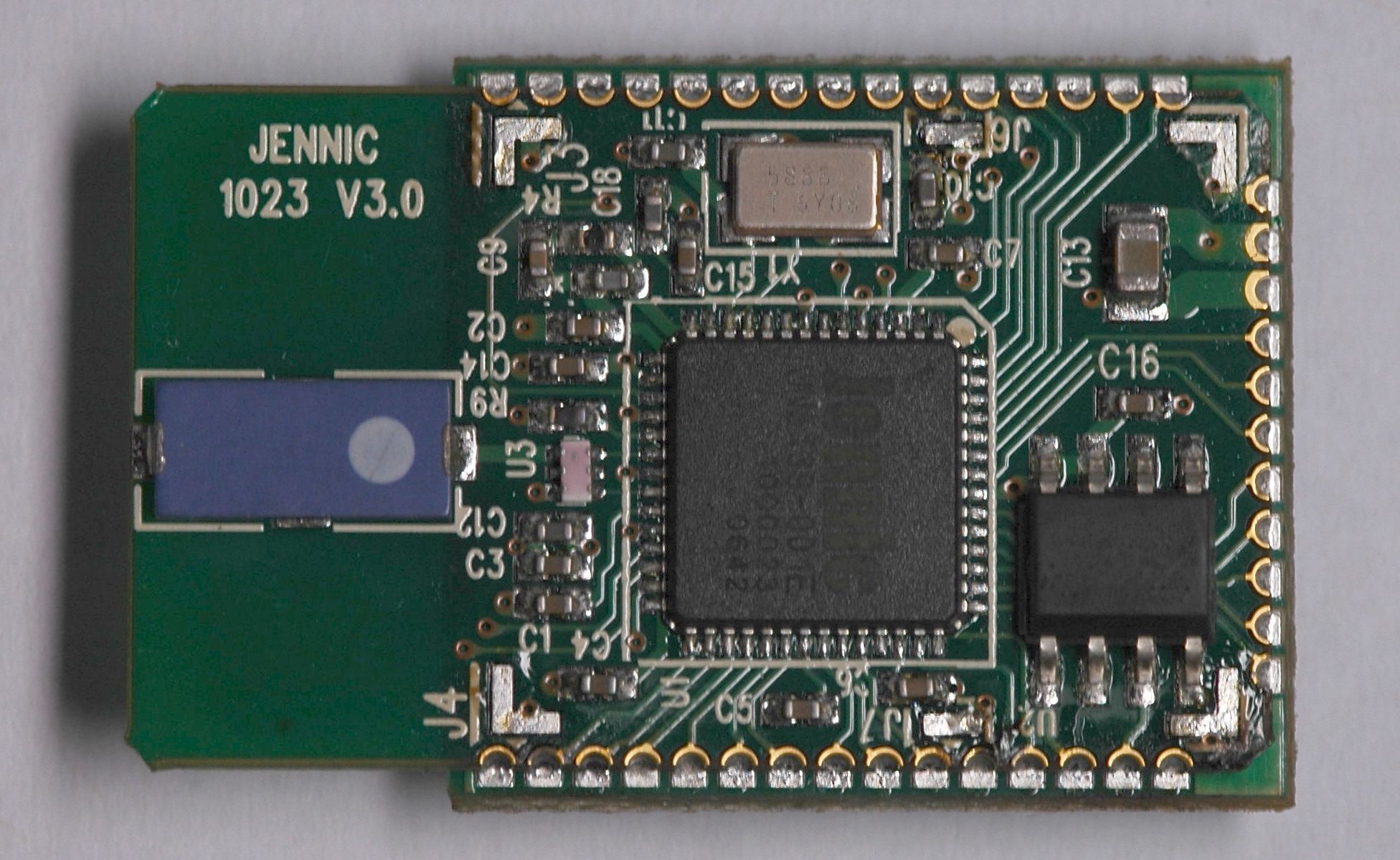
Item QTTY Component Reference Component Jennic Part No Description Reqd Notes Ordered Packed 1 10 C1,C2,C3,C4,C5,C6,C7,C14,C15,C16 100nF_0402 CP04100N Capacitor 100nF 0402 X5R 10 2 1 C8 330pF_0402 CP04330P Capacitor 330pF 0402 COG 1 3 1 C9 3n3_0402 CP0403N3 Capacitor 3.3nF 0402 X7R 1 4 2 C10,C11 15pF_0402 CP04015P Capacitor 15pF 0402 COG 2 5 1 C13 10uF_0805 CP08010U Capacitor 10uF 6.3V 0805 X5R 1 6 2 C12,C18 47pF_0402 CP04047P Capacitor 47pF 0402 NPO 2 7 1 J1 Ceramic_Antenna ANT00001 Ceramic Antenna 1 8 1 R4 4K7_0402 RE0404K7 Resistor 4K7 0402 1% 1 9 1 R9 43K_0402 RE04043K Resistor 43K 0402 1% 1 10 1 U1 JN5121 IC000001 IC JN5121 1 11 1 U2 M25P10_SO8 IC000014 IC Serial 3V Flash SMD M25P10-AVMN6P 1 12 1 U3 LDB182G4520C-110 BAL00001 Balun muRata LDB182G4520C-110 1 13 1 Y1 TSX-10A CRY00001 Crystal SMD TSX-10A (TSX-4025 TN4-25820) 1 14 1 PCB PCB PC000004 PCB for ZED Module (DR1023) 1 Assembly Description Revision Quantity Required Date DR1023 CA Module PCB 3.0 1 30/08/2006 Item Jennic Part No Description V alue 1 V alue 2 V alue 2 Package Supplier Supplier Part 1 CP04100N Capacitor 100nF 0402 X5R 100nF 10V X5R 0402 Flint CC0402AX5R104KTR 2 CP04330P Capacitor 330pF 0402 COG 330pF 50V COG 0402 Murata GRM1555C1H331JA01 3 CP0403N3 Capacitor 3.3nF 0402 X7R 3.3nF 50V X7R 0402 Flint 2238-587-15629 4 CP04015P Capacitor 15pF 0402 COG 15pF 0 C0G 0402 Flint MCH155A150J 5 CP08010U Capacitor 10uF 6.3V 0805 X5R 10uF 6.3V X5R 0805 Farnell InOne 922-7814 6 CP04047P Capacitor 47pF 0402 NPO 47pF 50V NPO 0402 Flint 2238-869-15479 7 ANT00001 Ceramic Antenna 2.45GHz 50R 100MHz 0 Farnell InOne 392-8081 8 RE0404K7 Resistor 4K7 0402 1% 4K7 0.063W 0.01 0402 Flint MCR01MZSEF4701 9 RE04043K Resistor 43K 0402 1% 43K 0.063W 0.01 0402 Flint MCR01MZSEF4302 10 IC000001 IC JN5121 JN5121 0 0 QFN56 Jennic 0 11 IC000014 IC Serial 3V Flash SMD M25P10-AVMN6P 128Kx8 0 0 SOIC Farnell InOne 866-1308 12 BAL00001 Balun muRata LDB182G4520C-110 2.4GHz 200R 50MHz LDB18 muRata LDB182G4520C-110 13 CRY00001 Crystal SMD TSX-10A (TSX-4025 TN4-25820) 16MHz 9pF 10ppm T SX-10 SM D Toyocom TSX-10A 16MHz 14 PC000004 PCB for ZED Module (DR1023) 0 0 0 0 Express Circuits DR1023 V3.0 Assembl y Description Revision Date DR1023 CA Module PCB 3.0 30/08/2006
RF Exposure Info
RF Exposure / MPE information Based on the fact that the module is intended for use only in mobile devices (not portable) the requirements are met without the need for MPE calculation. The transmitter is 2.4GHz; the 1500 - 100000 MHz exposure limit is 1.0mW/cm2 which equates to 5Watts @ 20cm distance. Therefore the unit must be compliant without need for calculation as the output power limit is only 1Watt. The actual device in question is much less than that at 0.1W maximum.
Schematics
DR1023.sch-1 - Thu Aug 31 08:55:22 2006
Test Report
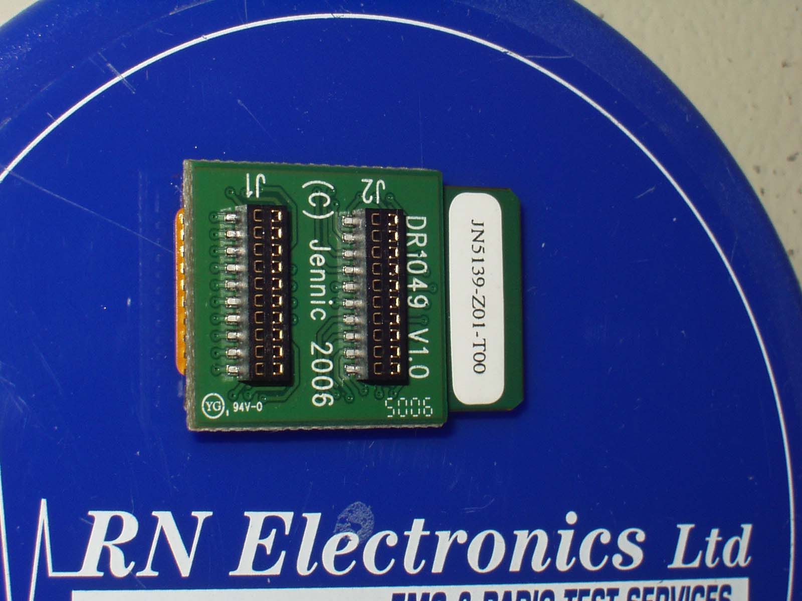
File name JENNIC.160A PAGE 1 OF 44 QMF21 – 8: FCC PART 15C: RNE ISSUE 02, APR 06 FCC Test Report for 802.15.4/ Zigbee module JN 5139-Z01-M00R Report Number 02-160A/3280/2/07 Supercedes report number 02-160/3280/2/07 Report Produced by: - R.N. Electronics Ltd. 1 Arnolds Court Arnolds Farm Lane Mountnessing ESSEX CM13 1UT www.RNelectronics.com Telephone 01277 352219 Facsimile 01277 352968 EMC & RADIO TEST SERVICES S RN Electronics ©2004 RN ELECTRONICS LIMITED REPORT NUMBER 02-160A/3280/2/07 ALL RIGHTS RESERVED File name JENNIC.160A PAGE 2 OF 44 QMF21 – 8: FCC PART 15C: RNE ISSUE 02, APR 06 1. Contents 1. CONTENTS............................................................................................................................................... 2 2. SUMMARY OF TEST RESULTS...................................................................................................................... 3 3. INFORMATION ABOUT EQUIPMENT UNDER TEST................................................................................... 4 4. SPECIFICATIONS....................................................................................................................................... 5 4.1 Deviations............................................................................................................................. 5 5. TESTS, METHODS AND RESULTS................................................................................................................. 6 5.1 Conducted Emissions ........................................................................................................... 6 5.2 Radiated Emissions............................................................................................................... 7 5.3 Intentional Radiator Field Strength ...................................................................................... 8 5.4 Maximum Spectral Power Density ....................................................................................... 9 5.5 6dB Bandwidth ...................................................................................................................10 6. PLOTS AND RESULTS............................................................................................................................. 11 6.1 Conducted Emissions ......................................................................................................... 11 6.2 Radiated Emissions.............................................................................................................11 6.3 6dB Bandwidth ...................................................................................................................34 7 EXPLANATORY NOTES.............................................................................................................................. 36 7.1 Explanation of FAIL LIMIT 1 Statement........................................................................... 36 7.2 Explanation of limit line calculations for radiated measurements ...................................... 36 8. PHOTOGRAPHS........................................................................................................................................... 37 8.1 Radiated emissions .............................................................................................................37 8.2 EUT .................................................................................................................................... 38 8.3 EUT in Test Jig................................................................................................................... 38 9. SIGNAL LEADS....................................................................................................................................... 40 10. TEST EQUIPMENT CALIBRATION LIST................................................................................................... 41 11. AUXILIARY EQUIPMENT........................................................................................................................ 42 11.1 Auxiliary equipment supplied by Jennic Ltd .................................................................. 42 11.2 Auxiliary equipment supplied by RN Electronics Limited............................................. 42 12. MODIFICATIONS.................................................................................................................................... 43 13. COMPLIANCE INFORMATION................................................................................................................. 44 ©2004 RN ELECTRONICS LIMITED REPORT NUMBER 02-160A/3280/2/07 ALL RIGHTS RESERVED File name JENNIC.160A PAGE 3 OF 44 QMF21 – 8: FCC PART 15C: RNE ISSUE 02, APR 06 2. Summary of Test Results The 802.15.4/ Zigbee module JN 5139-Z01-M00R was tested to the following standards: - FCC Part 15C (effective date February 7, 2007); Class DTS Intentional Radiator Any compliance statements are made reliant on: (a) the modes of operation as instructed to us by the Customer based on their specific knowledge of the application and functionality of the EUT. Title Reference Results 1. Conducted Emissions FCC Part 15C §15.207 NOT APPLICABLE 1 2. Radiated Emissions FCC Part 15C §15.205, §15.209 & §15.247(d) PASSED 3. Modulation Bandwidth FCC Part 15C §15.215(c), §15.247(a)(2) PASSED 4. Intentional Radiator Field Strength FCC Part 15C §15.247(b) PASSED 5. Power Spectral Density FCC Part 15C §15.247(e) PASSED This report relates to the equipment tested as identified by a unique serial number and at the time it was tested. It does not relate to any other similar equipment and performance of the product before or after the test cannot be guaranteed. Date of Test:23 rd March 2007 Test Engineer: Approved By: Customer Representative: 1 The digital device tested is intended to be powered from 3V dc supply (battery) and intended for modular approval. Any third party device it is incorporated into wi…
Text truncated - open the document above for the full version.
Test Report
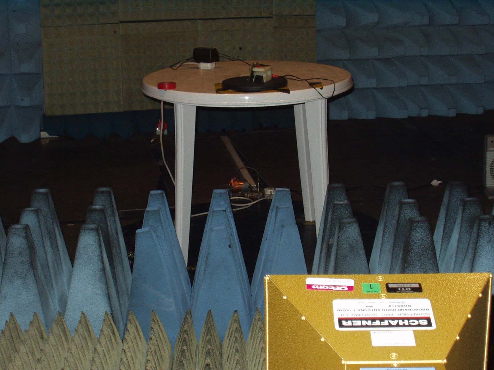
FILE NAME Jennic.160.SuppA Page 1 of 2 Supplement to Test Report Number 02-160/3280/2/07 Report Number 02-160/3280/2/07; Supplement A. Report Produced by: - R.N. Electronics Ltd. 1 Arnolds Court Arnolds Farm Lane Mountnessing ESSEX CM13 1UT www.RNelectronics.com Telephone 01277 352219 Facsimile 01277 35296 Manufacturer of EUT Jennic Ltd Furnival Street Sheffield S1 4QT Full name of EUT 802.15.4/ Zigbee module Model Number of EUT JN 5139-Z01-M00R Model Number of alternative sample JN 5130-000-M01 Serial Number of EUT 0704100031 Serial Number of alternative sample 004 FCC ID (if applicable): TYOJN5139M0 Date when equipment was received by RN Electronics Limited 9th February 2007 Date of test: 13th February 2007 Customer order number: PO 003971 Purpose: Additional information requested by TRL Compliance Services Ltd. EMC & RADIO TEST SERVICES S RN Electronics FILE NAME Jennic.160.SuppA Page 2 of 2 The following table lists the test equipment used, last calibration date and calibration interval. All equipment used has been maintained within the calibration requirements of R.N. Electronics Ltd. quality system. RNNo Model Description Manufacturer Last Cal Interval C031 437B Power Meter Hewlett Packard Sep-19-06 12 mths C032 8482A Power Sensor Hewlett Packard Sep-22-06 12 mths E1 HP8542E EMI Receiver & RF Filter Hewlett Packard Oct-31-06 12 mths E235 J2 7FV-15000/X6000 12-18 GHz BPF K&L Microwave Inc. N/A N/A E238 FC5343A 2.7 - 5.0 GHz BPF IFR N/A N/A E242 22102 Bandpass filter 7.8 - 16 GHz Merimec N/A N/A E246 8482B Power Sensor Hewlett Packard Nov-07-06 12 mths E268 BHA 9118 1-18 GHz Horn Antenna Schaffner May-26-06 60 mths E274 437B Power Meter Hewlett Packard Nov-07-06 12 mths E3 HP8593E Spectrum Analyser Hewlett Packard Sep-20-06 24 mths E5 HP8447F Pre-Amplifier Hewlett Packard Aug-15-06 12 mths N438 3513 172 1208 3.9 - 7.5 GHz BPF MEL N/A N/A TMS6-2 MS2602A Spectrum Analyser Anritsu Jan-25-07 24 mths TMS77 8673B Synthesised Signal Generator Hewlett Packard Nov-14-05 24 mths TMS79 460451 Std Gain Horn Antenna 18-26.5 GHz ETS Systems Oct-17-06 12 mths TMS82 8449B Pre Amplifier 1 - 26 GHz Agilent Oct-17-06 12 mths TMS933 CBL6141A Bilog Antenna 30MHz - 2GHz York EMC Aug17-06 36 mths Approved By: Technical Manager.
Contact Information
Applicant
Conrad Farlow
Technical Contact
Test Firm
R.N. Electronics Ltd.Roger Ray
Technical Specifications
| # | Rule Parts | Frequency Range | Power Output |
|---|---|---|---|
| 1 | 15C | 2.40 GHz - 2.48 GHz | 1.80 mW |
Other Applications from NXP Laboratories UK Ltd
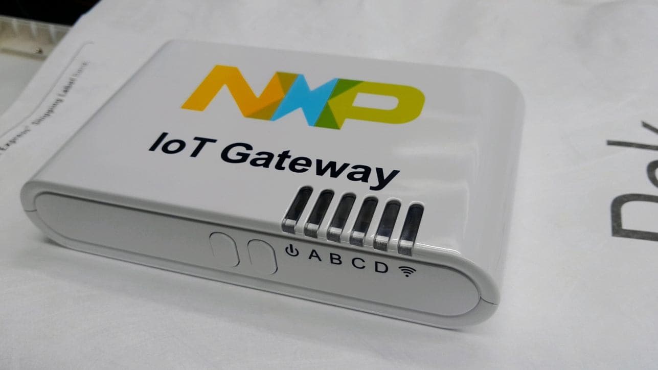
TYOJN5168IT00
Oct 22, 2013JN5168-RD6040-IoT Gateway
Equipment Class
DTS - Digital Transmission System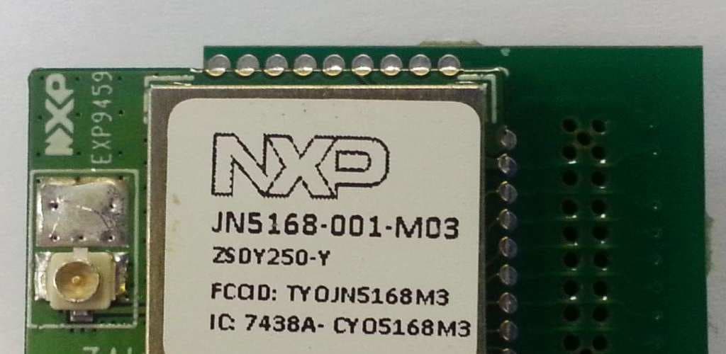
TYOJN5168M3
Jan 08, 2013JN5168-��1-M�3 IEEE802.15.4 Wireless Module
Equipment Class
DTS - Digital Transmission System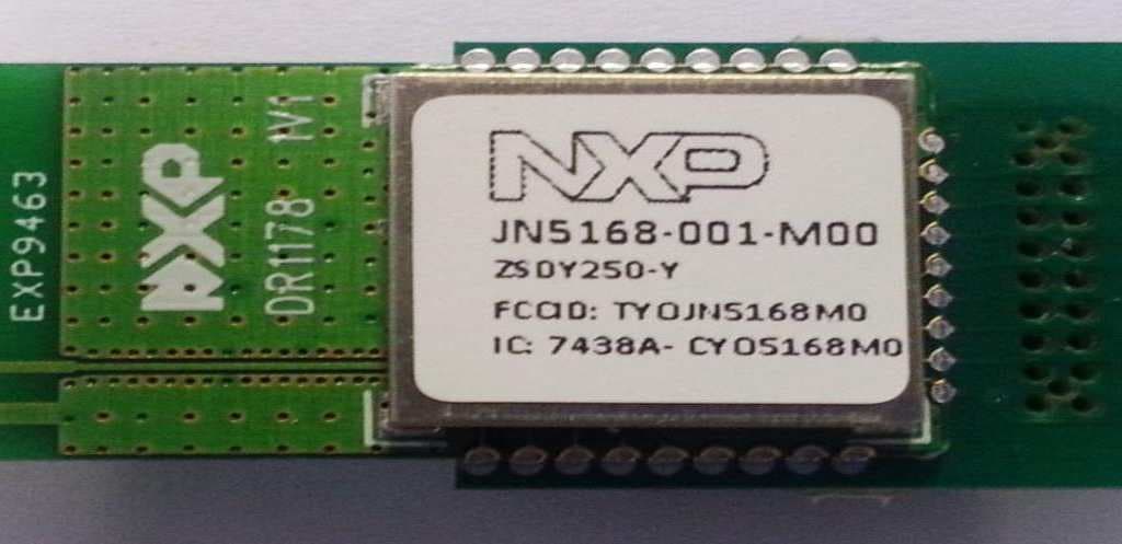
TYOJN5168M0
Jan 08, 2013JN5168-��1-M�� IEEE802.15.4 Wireless Module
Equipment Class
DTS - Digital Transmission System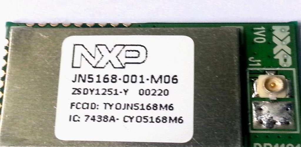
TYOJN5168M6
Jan 03, 2013JN5168-001-M�6 IEEE802.15.4 Wireless Module
Equipment Class
DTS - Digital Transmission System
TYOJN5168M5
Jan 03, 2013JN5168-001-M�5 IEEE802.15.4 Wireless Module
Equipment Class
DTS - Digital Transmission System