TYOJN5139M4JN5139-000-M04 IEEE802.15.4 Wireless Transmitter
NXP Laboratories UK Ltd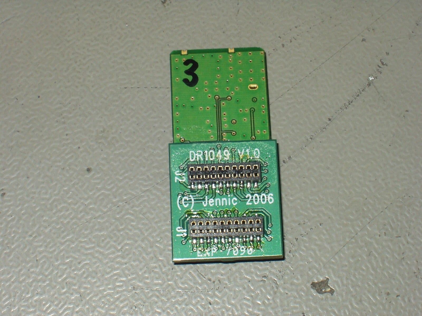
Click to zoom
Application Details
- Equipment Class
- DTS - Digital Transmission System
- Date of Grant
- Apr 18, 2007
- Application Purpose
- Original Equipment
- Date of Application
- Apr 18, 2007
- Equipment Note
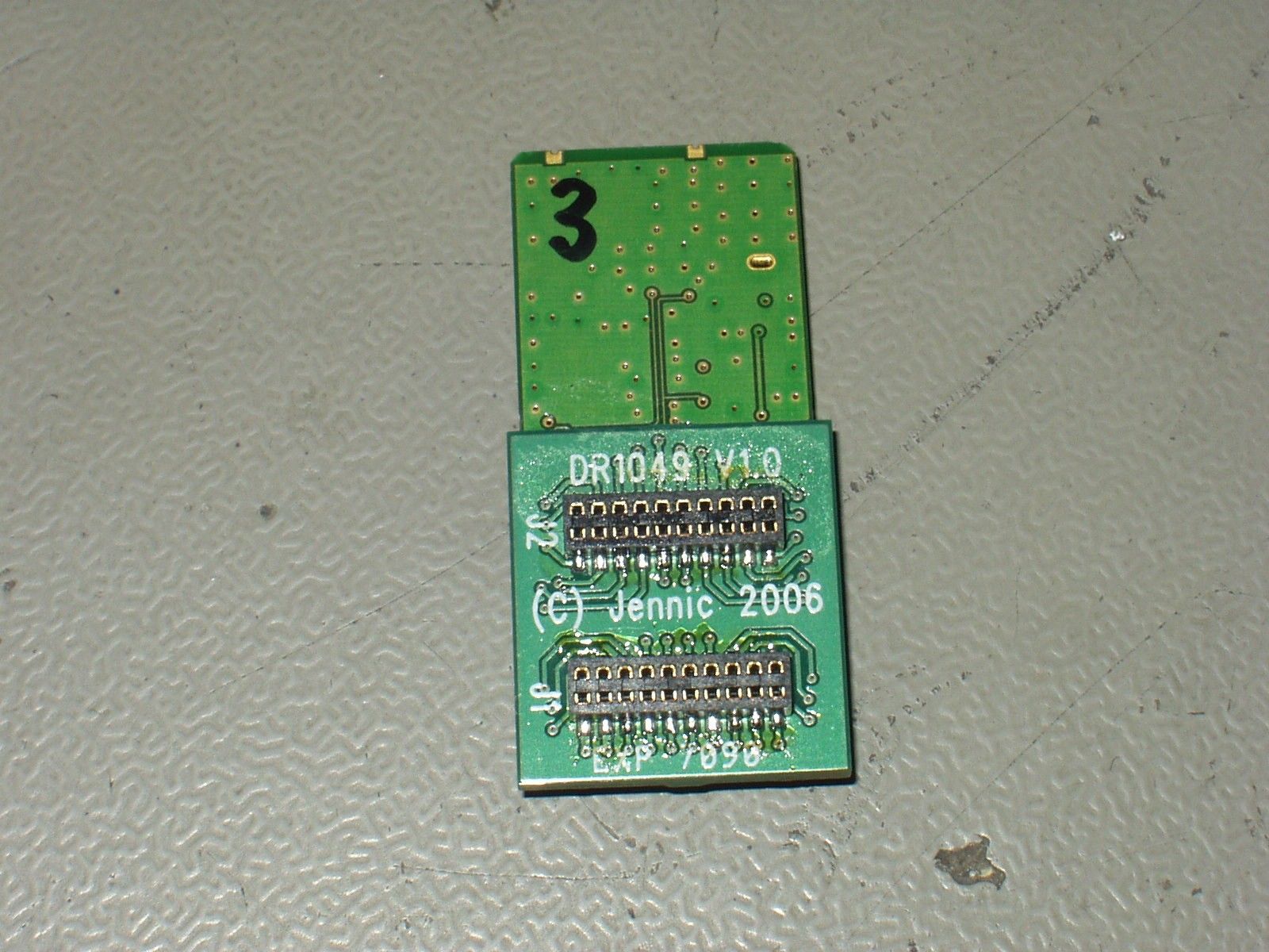
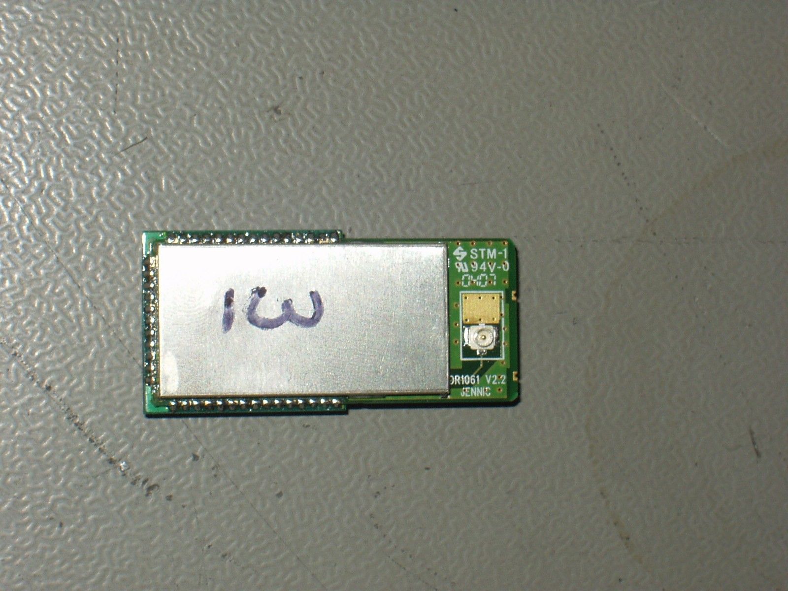
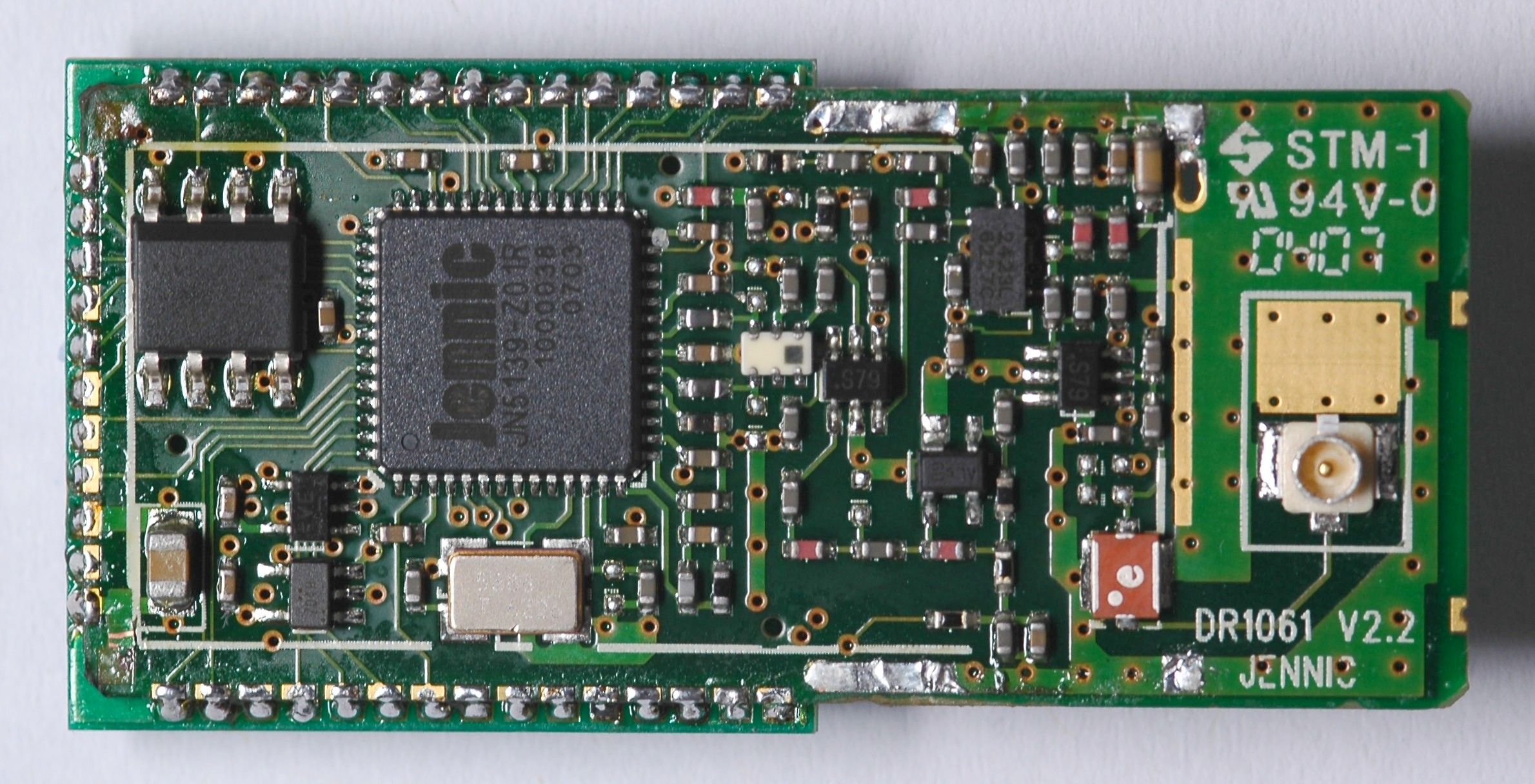
- JN5139-000-M04 IEEE802.15.4 Wireless Transmitter
- Frequency Range
- 2400.00000000 - 2483.50000000
- Company
- NXP Laboratories UK Ltd
- Country
- United Kingdom
Documents & Files
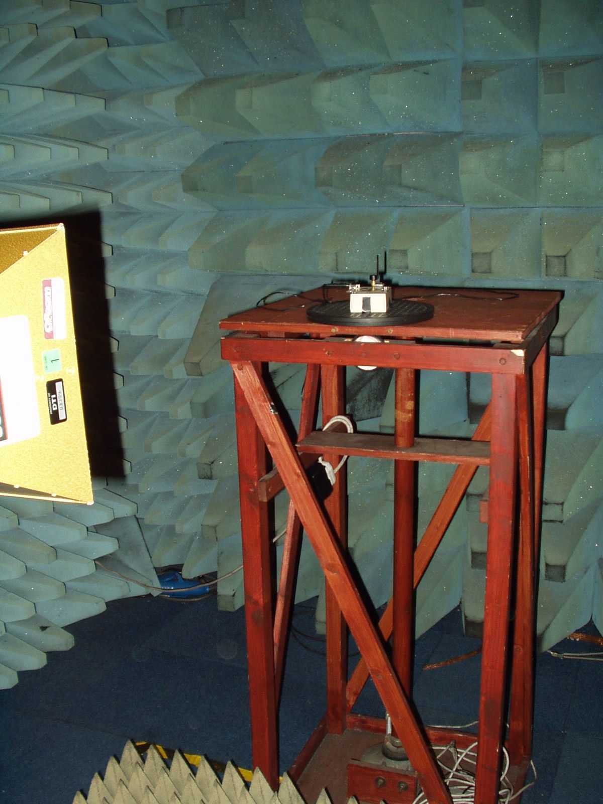
Document Text
Text extracted from the exhibit documents filed with the FCC. Open a document above to read the original.
Users Manual
Advanced Data Sheet – JN5139-xxx-Myy IEEE802.15.4/ZigBee Module Family Preliminary - JN-DS-JN5139-xxx-Myy v1.1 © Jennic 2007 Advanced Information Features: Module • 2.4GHz IEEE802.15.4 & ZigBee compliant • 2.7-3.6V operation • Sleep current (with active sleep timer) 2μA • JN5139-xxx-M00/01/03 > 1km range M00 has on board antenna M01 has SMA connector M03 has uFl connector o Receiver sensitivity -97dBm o TX power +3dBm o TX current < 39mA o RX current < 39mA o 18x30mm • JN5139-xxx-M02/04 > 4km range M02 has SMA connector M04 has uFl connector o Receiver sensitivity -100dBm o 19dBm TX power o TX current < 120mA o RX current < 45mA o 18x40.5mm Features: Microcontroller • 16MHz 32-bit RISC CPU • 96kB RAM, 192kB ROM • 4-input 12-bit ADC, 2 11-bit DACs, 2 comparators, temperature sensor • 2 Application timer/counters, 3 system timers • 2 UARTs (one for in-system debug) • SPI port with 5 selects • 2-wire serial interface • 21 GPIO • Evaluation kits available with full, unlimited, Software Development Kit Industrial temperature range (-20°C to +70°C) Lead-free and RoHS compliant Overview The JN5139-xxx-Myy family is a range of surface mount modules that enable users to implement IEEE802.15.4 or ZigBee compliant systems with minimum time to market and at the lowest cost. They remove the need for expensive and lengthy development of custom RF board designs and test suites. The modules use Jennic’s JN5139 wireless microcontroller to provide a comprehensive solution with high radio performance and all RF components included. All that is required to develop and manufacture wireless control or sensing products is to connect a power supply and peripherals such as switches, actuators and sensors, considerably simplifying product development. Three basic hardware module variants are available: JN5139-xxx-M00 with an integrated antenna, JN5139-xxx-M01/M03 with an antenna connector and JN5139- xxx-M02/M04 with a power amplifier and LNA for extended range. Each variant can be provided pre-programmed with a ZigBee network stack (JN5139-Z01-Myy). Module Block Diagram Benefits • Microminiature module solutions • Ready to use in products • Minimises product development time • No RF test required for systems • Compliant with FCC part 15 rules, ETSI ETS 300-328 and Japan ARIB STD-T66 • Production volumes supplied pre-programmed with application software Applications • Robust and secure low power wireless applications • Wireless sensor networks, particularly IEEE802.15.4 / ZigBee systems • Home and commercial building automation • Home networks • Toys and gaming peripherals • Industrial systems • Telemetry and utilities (e.g. AMR) Ti mers UARTs 12-bit ADC, comparators 11- bi t DACs, temp sensor 2-wire serial SPI RAM 96kB 128-bit AES Encr ypt i on Accelerator 2. 4GHz Radi o ROM 192kB RI SC CPU Power Management XTAL O- QPSK Modem IEEE802.15.4 MAC Accel erator 128kB Serial Fl ash Memory JN5139 chip Power Bal un Connector Bal un Cerami c Antenna Bal unConnectorPA / LNA Exter nal Ant enna M00 Option M01/03 Option M02/04 Option Jennic ii Preliminary - JN-DS-JN5139-xxx-Myy v1.1 © Jennic 2007 Contents 1. Introduction 3 1.1. Variants 3 1.2. Regulatory Approvals 3 2. Specifications 4 3. Product Development 5 3.1. JN5139 Single Chip Wireless Microcontroller 5 4. Pin Configurations 6 4.1. Pin Assignment 7 4.2. Pin Descriptions 8 4.3. Power Supplies 8 4.4. SPI Memory Connections 8 5. Electrical Characteristics 9 5.1. Maximum Ratings 9 5.2. Operating Conditions 9 Appendix A Additional Information 10 A.1 Outline Drawing 10 A.2 Module PCB Footprint 15 A.3 Ordering Information 16 A.4 Tape and Reel Information: 17 A.4.1 Tape Orientation and dimensions 17 A.4.2 Cover tape details 17 A.4.3 Leader and Trailer 18 A.4.4 Reel Dimensions: 18 A.5 Related Documents 19 A.6 Federal Communication Commission Interference Statement 19 A.7 RoHS Compliance 20 A.8 Status Information 20 A.9 Disclaimers 21 A.10 Version Control 21 A.11 Contact Details 22 Jennic © Jennic 2007 Preliminary - JN-DS-JN5139-xxx-Myy v1.1 3 1. Introduction The JN5139-xxx-Myy module family provides designers with a ready made component which allows IEEE802.15.4 [1] wireless applications, including ZigBee, to be quickly and easily included in product designs. The modules integrate all of the RF components, removing the need to perform expensive RF design and test. Products can be designed by simply connecting sensors and switches to the module IO pins. The modules use Jennic’s single chip IEEE802.15.4 Wireless Microcontroller, allowing designers to make use of the extensive chip development support material. Hence, this range of modules allows designers to bring wireless applications to market in the minimum time with significantly reduced development effort and cost. Three basic module hardware variants are available: JN5139-xxx-M00 (standard module with on board ceramic antenna), JN5139-xxx-M01 (standard module with SMA connector for use with external antennae) and JN5139-xxx- M02 (high RF power, improved sensitivity module for extended range applications). uFL connector variants are provided (-M03 standard power and –M04 high power) for FCC approved products and for applications where a small connector size is required. Each of these modules can be supplied with a range of protocol stacks, including a simple IEEE802.15.4 protocol for point to point and star applications and a ZigBee mesh networking stack. The variants available are described below. 1.1. Variants 1.2. Regulatory Approvals All module types have been tested against the requirements of European standard ETS 300 328 and a certificate of compliance to this standard is available on request. The High Power modules with M02 suffix are approved for use in Europe with reduced output power. They must not be used with PHY_PIB_ATTR_TX_POWER set above 3 See [4]. Additionally, modules with M00, M03 and M04 suffixes have received FCC “Modular Approvals”, in compliance with CFR 47 FCC part 15 regulations and in accordance to …
Text truncated - open the document above for the full version.
Block Diagram
RADIO BLOCK DIAGRAM The radio comprises a low-IF receive path and a direct up-conversion transmit path, which converge at the TX/RX switch. This switch includes the necessary matching components such that a 200Ω differential antenna may be directly connected without external components. Alternatively, a balun can be used for single ended antennas. The 16MHz crystal oscillator feeds a divider, which provides the frequency synthesiser with a reference frequency. The synthesiser contains programmable feedback dividers, phase detector, charge pump and internal Voltage Controlled Oscillator (VCO). The VCO has no external components, and includes calibration circuitry to compensate for differences in internal component values due to process and temperature variations. The VCO is controlled by a Phase Lock Loop (PLL) that has a loop filter comprising 3 external components. A programmable charge pump is also used to tune the loop characteristic. Finally, quadrature (I and Q) local oscillator signals for the mixer drives are derived. The receiver chain starts with the low noise amplifier / mixer combination whose outputs are passed to the polyphase bandpass filter. This filter provides the channel definition as well as image frequency rejection. The signal is then passed to two variable gain amplifier blocks. The gain control for these stages, and the bandpass filter, is derived in the automatic gain control (AGC) block within the Modem. The signal is conditioned with the anti-alias low pass filter, before being converted to a digital signal with a flash ADC. In the transmit direction, the digital I and Q streams from the Modem are passed to I and Q quadrature DAC blocks which are buffered and low-pass filtered, before being applied to the modulator mixers. The summed 2.4 GHz signal is then passed to the RF Power Amplifier (PA), whose power control can be selected from one of six settings. The output of the PA drives the antenna via the RX/TX switch. 1600 MHz 1600 MHz 3MHz 1600 MHz
Cover Letter(s)
Polar Plots and VSWR Graph Antenna Factor575 S.E. Ashley Place Grants Pass, OR 97526-3237 www.antennafactor.com 541-956-0931 (phone) 541-471-6251 (fax) Rev 04-27-06 Typical VSWR ANT-2.4-CW-RCL DATA SHEETS Product DimensionsDescription Features Electrical Specifications Ordering Information AzimuthElevation -50.0 -40.0 -30.0 -20.0 -10.0 0.0 -45.0 -35.0 -25.0 -15.0 -5.0 5.0 0.24” (6.0) 0.31” (8.0) 0.42” (10.6) The RCL Series is useful in products where additional height above the product’s case is needed or a slightly wider operational bandwidth is desired. The 2.45GHz version has a center-fed 1/2-wave element with an internal ground reference. Right-angle mount Excellent performance Omni-directional pattern Fully weatherized Rugged & damage-resistant Part 15 compliant RP-SMA connector Available in black or custom colors Use with plastic or metal enclosures Center Freq. Bandwidth Wavelength VSWR Impedance Gain Connector Electrical specifications and plots measured on 4.00” x 4.00” reference ground plane ANT-2.4-CW-RCL CENTER 2 450.000MHz SPAN 1 000.000MHz S11 SWR 1.470 3.46” (88.0) 2.45GHz 120MHz 1/2-wave <1.7 typ. at center 50 ohms 2.90dBi RP-SMA Absolute Gain of AUT -50.0 -40.0 -30.0 -20.0 -10.0 0.0 0 90 180 270 90° 270° 180° 0° Antenna Antenna Factor575 S.E. Ashley Place Grants Pass, OR 97526-3237 www.antennafactor.com 541-956-0931 (phone) 541-471-6251 (fax) ANT-2.4-CW-RCL DATA SHEETS Azimuth Radiation Pattern Elevation Radiation Pattern Absolute Gain of AUT -45.0 -35.0 -25.0 -15.0 -5.0 5.0 0 90 180 270 90° 270° 180° 0° Antenna Measurement Antenna Polarity: Vertical Test Antenna Polarity: Vertical Maximum Absolute Gain: -0.50dBi Measurement Antenna Polarity: Horizontal Test Antenna Polarity: Horizontal Maximum Absolute Gain: 2.90dBi 4.00” (101.6) 4.00” (101.6) GROUND PLANE ON BOTTOM LAYER Antenna Test Fixture The adjoining diagram shows the dimensions of the fixture on which the stated pattern and gain measurements were made. This does not mean that your product must conform to this size or antenna orientation, although it should be recognized that the gain, pattern, and performance may increase or decrease accordingly. Antenna Factor recognizes that our antennas are often used in compact applications with less than ideal ground planes. In some cases, the reference jig is smaller than optimum, particularly with lower-frequency antennas. This is, in part, to more accurately reflect the performance of the antenna in typical real-world applications. ABOUT THIS TEST FIXTURE
Cover Letter(s)
Polar Plots and VSWR Graph Antenna Factor575 S.E. Ashley Place Grants Pass, OR 97526-3237 www.antennafactor.com 541-956-0931 (phone) 541-471-6251 (fax) Rev 05-01-06 Typical VSWR ANT-2.4-CW-RCT-xx DATA SHEETS Product DimensionsDescription Features Electrical Specifications Ordering Information AzimuthElevation -45.0 -35.0 -25.0 -15.0 -5.0 5.0 9 -45.0 -35.0 -25.0 -15.0 -5.0 5.0 The RCT 1/2-wave 2.4GHz antenna delivers outstanding performance and orientation flexibility in a compact physical package. The antenna’s innovative articulating base allows it to tilt and swivel for optimum orientation. The RCT mounts quickly via an SMA or FCC Part 15 compliant RP-SMA connector. Tilts and rotates Very low VSWR Excellent performance Omni-directional pattern Fully weatherized Rugged and damage-resistant RP-SMA or SMA connector 0.35” (9.0) 0.39” (10.0) 0.33” (8.4) 3.76” (95.6) 0.20” (5.1) 1.10” (28.0) 4.44” (113.0) Center Freq. Bandwidth Wavelength VSWR Impedance Gain Connector 2.45GHz 120MHz 1/2-wave <1.9 typ. at center 50 ohms 2.20dBi RP-SMA or SMA Electrical specifications and plots measured on 4.00” x 4.00” reference ground plane CENTER 2 450.000MHz SPAN 200.000MHz S11 SWR 1.033 ANT-2.4-CW-RCT-RP (with RP-SMA connector) ANT-2.4-CW-RCT-SS (with SMA connector) Absolute Gain of AUT -45.0 -35.0 -25.0 -15.0 -5.0 5.0 0 90 180 270 90° 270° 180° 0° Antenna Antenna Factor575 S.E. Ashley Place Grants Pass, OR 97526-3237 www.antennafactor.com 541-956-0931 (phone) 541-471-6251 (fax) ANT-2.4-CW-RCT-xx DATA SHEETS Azimuth Radiation Pattern Elevation Radiation Pattern Absolute Gain of AUT -45.0 -35.0 -25.0 -15.0 -5.0 5.0 0 90 180 270 90° 270° 180° 0° Antenna Measurement Antenna Polarity: Vertical Test Antenna Polarity: Vertical Maximum Absolute Gain: 0.40dBi Measurement Antenna Polarity: Horizontal Test Antenna Polarity: Horizontal Maximum Absolute Gain: 2.20dBi 4.00” (101.6) 4.00” (101.6) GROUND PLANE ON BOTTOM LAYER Antenna Test Fixture The adjoining diagram shows the dimensions of the fixture on which the stated pattern and gain measurements were made. This does not mean that your product must conform to this size or antenna orientation, although it should be recognized that the gain, pattern, and performance may increase or decrease accordingly. Antenna Factor recognizes that our antennas are often used in compact applications with less than ideal ground planes. In some cases, the reference jig is smaller than optimum, particularly with lower-frequency antennas. This is, in part, to more accurately reflect the performance of the antenna in typical real-world applications. ABOUT THIS TEST FIXTURE
Cover Letter(s)
Specifications subject to change without notice. 3425 N.44 th Street, LINCOLN, NE 68504 USA SALES PHONE: 800.228.4563 PHONE: 402.467.4491 • FAX: 402.467.4528 www.centurion.com • [email protected] Copyright 2004 Centurion Wireless Technologies, Inc. All Rights Reserved Specifications: ½ wave coaxial dipole Clutch allows 360º rotation Flexible element FCC Part 15 compliant polarized connector Frequency 2.4 – 2.5 GHz Polarization Vertical MMCX 1.0 dBi SMA 2.0 dBi Gain SMRP 1.0 dBi Nominal Impedance 50 ohms VSWR 1.5:1 max at resonance RF Power Handling 50 watts Size (Length) 8cm Temperature Range -40° to +80°C Drop Test 1M Connectors: Model # Part # Connector WCR2400-MMCX WCR2400MMCX MMCX Straight WCR2400-SMA WCR2400SMA SMA-Male WCR2400-SMRP WCR2400SMRP RP-SMA-Male (gold) WCRb – 1/17/05 WCR Model Number: WCR2400 External Antenna – Connector Mount 10 cm 8 cm Azimuth WCR2400MMCX Elevation WCR2400MMCX
Cover Letter(s)
Specifications subject to change without notice. 3425 N.44 th Street, LINCOLN, NE 68504 USA SALES PHONE: 800.228.4563 PHONE: 402.467.4491 • FAX: 402.467.4528 www.centurion.com • [email protected] Copyright 2004 Centurion Wireless Technologies, Inc. All Rights Reserved Specifications: Covers 802.11b for all U.S., European & Japanese WLAN applications Center fed coaxial dipole Frequency 2.4 – 2.5 GHz Gain 1.3 dBi (2.45 GHz) Polarization Vertical, Omnidirectional Nominal Impedance 50 ohms VSWR 2:1 max across all bands Size (Length) 10.9 cm (180°) or 8.8 cm (90°) Connectors: Model # Part # Color Connector WRR2400-RPSMA-B MAF94028 Black RP-SMA WRR2400-RPSMA-G MAF94046 Gray RP-SMA WRR RPSMAa – 5/18/04 WRR - RPSMA Model Number: WRR2400-RPSMA External Antenna – Connector Mount Elevation Plane phi = 0 2.45 GHz Elevation Plane phi = 90 2.45 GHz Azimuth Plane 2.45 GHz 8.8 cm 8.8 cm
Cover Letter(s)
Product Specification Product Specification Titanis 2.4 GHz Swivel SMA Antenna Rev : AE030054-B / April 18 2005 Titanis 2.4 GHz Swivel SMA Antenna 2 (7)Subject to changes without prior notice 1. FEATURES -Designed for 2.4 GHz applications [Bluetooth TM , WiFi TM (802.11b/g), Zigbee TM , WiMedia TM etc.] - Also available as reversed thread (left) to meet FCC regulation part 15 - Intended for SMA mounting - Supplied in bulk 2. DESCRIPTION - Development tools - Test equipment - Instruments - Access points and gateways - Printers 3. APPLICATION The Titanis antenna is intended for use with all 2.4 GHz applications. The antenna is fitted with an SMA male connector and a blade, made of a flexible material that can be rotated 360 degrees. No external matching net is required. Titanis is available as standard SMA and reversed thread SMA. TABLE OF CONTENT 1. Features ......................................................................................................................................................................... 2 2. Description ..................................................................................................................................................................... 2 3. Application ...................................................................................................................................................................... 2 4. General data ................................................................................................................................................................... 3 5. Model names .................................................................................................................................................................. 3 6. Electrical characteristics ................................................................................................................................................. 3 7. Electrical performance .................................................................................................................................................... 4 7.1 Voltage Standing Wave Ratio ............................................................................................................................... 4 7.2 Radiation patterns ................................................................................................................................................ 4 7.3 3D-Radiation ........................................................................................................................................................ 4 8. Antenna Dimensions ....................................................................................................................................................... 5 9. Electrical interface .......................................................................................................................................................... 5 9.1 Connection ........................................................................................................................................................... 5 9.2 Electrical performance test set-up ........................................................................................................................ 5 10. Reliability ...................................................................................................................................................................... 6 10.1 Temperature and Humidity ................................................................................................................................. 6 10.2 Judgement standard .......................................................................................................................................... 6 11. Hazardous Material Reguration Conformance .............................................................................................................. 6 12. Packaging ..................................................................................................................................................................... 7 12.1 Shelf storage recommendation .......................................................................................................................... 7 12.2 Packaging characteristics .................................................................................................................................. 7 12.3 Bag label information ......................................................................................................................................... 7 13. Contact information ...................................................................................................................................................... 7 Rev : AE030054-B / April 18 2005 Titanis 2.4 GHz Swivel SMA Antenna 3 (7)Subject to changes without prior notice 5. GENERAL DATA 20 10 Bxxxx - 01 4. MODEL NAMES Antenna Family -External Technology -Metal Drawing No. 6. ELECTRICAL CHARACTERISTICS emaNtcudorPzHG4.2sinatiT .oNelcitrA )dradnatS(10-4484B0102 )daerhtesreveR(10-0906B0102 ycneuqerFzHG5.2-4.2 noitaziraloPraeniL erutarepmetgnitarepOCged58+ot04- ecnadepmImhO05 thgieWmarg4.7 epytannetnAleviwS scitsiretcarahC *snoitidnoC niMpyTxaM niaGkaePiBd0.4iBd1.4iBd4.4 )dleifraen(rebmahcD3niderusaeM,zHG5.2-4.2ycneuqerF ycneiciffE%08%58%09 RWSV1:1.11:2.11:3.1rezylanAkrowteNniderusaeM,zHG5.2-4.2ycneuqerF draobecnerefertnAagigehtnodesaberaelbatsihtnidedivorpatadllaetoN* Rev : AE030054-B / April 18 2005 Titanis 2.4 GHz Swivel SMA Antenna 4 (7)Subject to changes without prior notice 7.3 Radiation patterns XY- Plane XZ- Plane YZ- Plane To t a l polarization 7.1 Voltage Standing Wave Ratio 7. ELECTRICAL PERFORMANCE 7.2 3D-Radiation Vertical polarization Horizontal polarization Rev : AE030054-B / April 18 2005 Titanis 2.4 GHz Swivel SMA Antenna 5 (7)Subject to changes without prior notice 8. ANTENNA DIMENS…
Text truncated - open the document above for the full version.
Cover Letter(s)
e-mail: [email protected] • tel: 561-995-2256 • fax: 561-995-2432 web: www.hyperlinktech.com • 1201 Clint Moore Road • Boca Raton FL 33487 2.4 GHz 2.2 dBi Reverse Polarity SMA "Rubber Duck" Wireless LAN Antenna Features • Compact size, only 4.7" long • Tilt and swivel design • RP-SMA Connector • 802.11b, 802.11g and Bluetooth® compatible Model: HG2402RD-RSF Description This compact 2.4GHz omnidirectional "rubber-duck" WiFi antenna provides broad coverage and 2.2 dBi gain. It is a coaxial sleeve design with an omni-directional pattern. It is ideally suited for IEEE 802.11b and 802.11g wireless LANs, Bluetooth® and other WLAN applications. Only 4.7" long, this flexible antenna features a tilt-and-swivel reverse-polarity SMA plug connector, allowing them to be used vertically, at a right angle, or any angle in-between. It is suitable as a replacement antenna for many access points and radios that are equipped with reverse-polarity SMA connectors including D-Link®, Linksys® WET11 and others (Note: This RF antenna is used as a "replacement" antenna rather than a "range extender" antenna. It should yield similar range to most radio's stock antennas). Application Note: This antenna is not for use with U.S.Robotics® RP-SMA equipped devices. Specifications Electrical Specifications Frequency 2400-2500 MHz Gain 2.2 dBi Impedance 50 Ohm VSWR < 2.0 Mechanical Specifications Weight 0.52 oz. (15 g) Length 4.7" (105 mm) Diameter 0.4" (10 mm) Finish Matte Black Connector Reverse Polarity SMA Plug Operating Temperature -40° C to to 85° C (-40° F to 185° F) Polarization Vertical RoHS Compliant Yes e-mail: [email protected] • tel: 561-995-2256 • fax: 561-995-2432 web: www.hyperlinktech.com • 1201 Clint Moore Road • Boca Raton FL 33487 Antenna Gain Pattern
ID Label/Location Info
JN5139-XXX-M04 Module Labelling Location: JN5139-000-M04 Subsequent to being granted an FCC-ID the following label will be used for JN5139- 000-M04. Product Identification Instructions Label line 1: FCC ID Number Label line 2: Part Name Label line 3: Barcode Label line 4: YYWWTNNNNN (see below) Identifier Description Format YY Year 06(example) WW Week 45(example) T Module type 0 NNNNN Serial Number FCCID: TYOJN5139M4 YYWWTNNNNN JN5139-000-M04 Label Placed Here. 1 JN5139-Z01-M04 Subsequent to being granted an FCC-ID the following label will be used for JN5139- Z01-M04. Product Identification Instructions Label line 1: FCC ID Number Label line 2: Part Name Label line 3: Barcode Label line 4: YYWWTNNNNN (see below) Identifier Description Format YY Year 06(example) WW Week 45(example) T Module type 1 NNNNN Serial Number 1 JN5139_XXX_M04_FCC_label_1v2.doc CF. FCCID: TYOJN5139M4 YYWWTNNNNN JN5139-Z01-M04
Operational Description
RADIO BLOCK DIAGRAM The radio comprises a low-IF receive path and a direct up-conversion transmit path, which converge at the TX/RX switch. This switch includes the necessary matching components such that a 200Ω differential antenna may be directly connected without external components. Alternatively, a balun can be used for single ended antennas. The 16MHz crystal oscillator feeds a divider, which provides the frequency synthesiser with a reference frequency. The synthesiser contains programmable feedback dividers, phase detector, charge pump and internal Voltage Controlled Oscillator (VCO). The VCO has no external components, and includes calibration circuitry to compensate for differences in internal component values due to process and temperature variations. The VCO is controlled by a Phase Lock Loop (PLL) that has a loop filter comprising 3 external components. A programmable charge pump is also used to tune the loop characteristic. Finally, quadrature (I and Q) local oscillator signals for the mixer drives are derived. The receiver chain starts with the low noise amplifier / mixer combination whose outputs are passed to the polyphase bandpass filter. This filter provides the channel definition as well as image frequency rejection. The signal is then passed to two variable gain amplifier blocks. The gain control for these stages, and the bandpass filter, is derived in the automatic gain control (AGC) block within the Modem. The signal is conditioned with the anti-alias low pass filter, before being converted to a digital signal with a flash ADC. In the transmit direction, the digital I and Q streams from the Modem are passed to I and Q quadrature DAC blocks which are buffered and low-pass filtered, before being applied to the modulator mixers. The summed 2.4 GHz signal is then passed to the RF Power Amplifier (PA), whose power control can be selected from one of six settings. The output of the PA drives the antenna via the RX/TX switch. 1600 MHz 1600 MHz 3MHz 1600 MHz
Parts List/Tune Up Info
Item QTTY Component Reference Component Jennic Part No Description Reqd Notes 1 16 C1-4, C6-8, C10, C12, C17, C18, C27, C31, C39, C42, C46 100nF_0402 CP04100N Capacitor 100nF 0402 X5R 16 2 1 C16 330pF_0402 CP04330P Capacitor 330pF 0402 COG 1 3 1 C19 3n3_0402 CP0403N3 Capacitor 3.3nF 0402 X7R 1 4 15 C11, C13, C15, C21, C22, C24, C25, C28, C29, C37, C40, C41, C44, C45, C48 15pF_0402 CP04015P Capacitor 15pF 0402 COG 15 5 1 C5 10uF_0805 CP08010U Capacitor 10uF 6.3V 0805 X5R 1 6 2 C47, C50 100pF_0402 CP04100P Capacitor 100pF 0402 COG 2 7 1 C23 10nF_0402 CP04010N Capacitor 10nF 0402 X7R 1 8 1 C34 1pF_0402 CP04001P Capacitor 1pF 0402 NPO 1 9 2 C26, C30 10pF_0402 CP04010P Capacitor 10pF 0402 NPO 2 10 1 C43 2.2uF_0603 CP0602U2 Capacitor 2.2uF 0603 X5R 1 11 1 C32 4.7pF_0402 CP0404P7 Capacitor 4.7pF 0402 NPO 1 12 2 C36, C38 5.6pF_0402 CP0405P6 Capacitor 5.6pF 0402 NPO 2 13 1 C49 0.5pF_0402 CP0400P5 Capacitor 0.5pF 0402 COG 1 14 1 R2 4K7_0402 RE0404K7 Resistor 4K7 0402 1% 1 15 1 R1 43K_0402 RE04043K Resistor 43K 0402 1% 1 16 1 R5 22K_0402 RE04022K Resistor 22K 0402 1% 1 17 2 R3, R4 47R_0402 RE04047R Resistor 47R 0402 1% 2 18 1 R9 2R2_0402 RE0402R2 Resistor 2R2 0402 1% 1 19 1 R6' 10R_0402 RE04010R Resistor 10R 0402 1% 1 20 2 L1, L2 0R_0402 RE04000R Resistor 0R 0402 1% 2 21 1 L7 1.8nH_0402 IND001N8 Inductor 1.8nH 1 22 1 L10 100nH_0402 IND0100N Inductor 100nH 1 23 1 L6 10nH_0402 IND0010N Inductor 10nH 1 24 1 L8 2.7nH_0402 IND002N7 Inductor 2.7nH 1 25 1 L4 3.3nH_0402 IND003N3 Inductor 3.3nH 1 26 1 L5 33nH_0402 IND0033N Inductor 33nH 1 27 1 Q1 BFP405_SOT343 TN000003 Transistor, RF, NPN, BFP405 1 28 1 T1 HHM1521 BAL00003 Balun TDK HHM1521 1 29 1 Y1 TSX-10A CRY00001 Crystal SMD TSX-10A (TSX-4025 TN4-25820) 1 30 1 U9 UFL_SM CN000056 UFL Connector 1 31 1 U3 JN5139 IC000031 IC JN5139 1 32 1 U1 SST25VF010A IC000032 IC Serial 3V Flash SMD SST25VF010A-33-4I-SAE 1 33 1 U2 NC7SZ04 IC000019 IC Invertor NC7SZ04 1 34 1 U8 74LV1G08 IC000020 74AHCT1G08 Logic single gate 1 35 1 U7 PA2423L IC000033 IC Power Amp 2.4GHz 1 36 1 U6 MDR774M IC000034 Filter Band Pass 2450MHz 25dB 1 37 2 U4, U5 AS179-92 IC000035 IC MMIC SW SPDT SC-70-6P 2 38 1 PC000024 PCB for High Power UFL Module (DR1061) 1 39 C9, C14, C20, C33, C35, R6, R7, R8, L9 Not Fitted Parts Not To Be Fitted 0 Assembly Description Revision Quantity Required Date DR1061 High power UFL module 2.2 1 10/01/2007 Item Jennic Part No Description Value 1 Value 2 Value 2 Package Supplier Supplier Part 1 CP04100N Capacitor 100nF 0402 X5R 100nF 10V X5R 0402 Flint CC0402AX5R104KTR 2 CP04330P Capacitor 330pF 0402 COG 330pF 50V COG 0402 Murata GRM1555C1H331JA01 3 CP0403N3 Capacitor 3.3nF 0402 X7R 3.3nF 50V X7R 0402 Flint 2238-587-15629 4 CP04015P Capacitor 15pF 0402 COG 15pF 0 C0G 0402 Flint MCH155A150J 5 CP08010U Capacitor 10uF 6.3V 0805 X5R 10uF 6.3V X5R 0805 Farnell InOne 922-7814 6 CP04100P Capacitor 100pF 0402 COG 100pF 50V COG 0402 Flint MCH155A101J 7 CP04010N Capacitor 10nF 0402 X7R 10nF 16V X7R 0402 Farnell InOne 301-9275 8 CP04001P Capacitor 1pF 0402 NPO 1pF 0 NPO 0402 Farnell InOne 3019-100 9 CP04010P Capacitor 10pF 0402 NPO 10pF 0 NPO 0402 Farnell InOne 3019-160 10 CP0602U2 Capacitor 2.2uF 0603 X5R 2.2uF 10V X5R 0603 Murata G RM188R61C225KE1 5 11 CP0404P7 Capacitor 4.7pF 0402 NPO 4.7pF 0 NPO 0402 RS 456-8617 12 CP0405P6 Capacitor 5.6pF 0402 NPO 5.6pF 0 NPO 0402 Farnell InOne 7568-088 13 CP0400P5 Capacitor 0.5pF 0402 COG 0.5pF 0 C0G 0402 0 GRM1555C1HR50C 14 RE0404K7 Resistor 4K7 0402 1% 4K7 0.063W 0.01 0402 Flint MCR01MZSEF4701 15 RE04043K Resistor 43K 0402 1% 43K 0.063W 0.01 0402 Flint MCR01MZSEF4302 16 RE04022K Resistor 22K 0402 1% 22K 0.063W 0.01 0402 Farnell InOne 9232-923 17 RE04047R Resistor 47R 0402 1% 47R 0.063W 0.01 0402 Farnell InOne 1174-145 18 RE0402R2 Resistor 2R2 0402 1% 2R2 0.063W 0.01 0402 Flint 2322-706-72208 19 RE04010R Resistor 10R 0402 1% 10R 0.063W 0.01 0402 Farnell InOne 360-3088 20 RE04000R Resistor 0R 0402 1% 0R 0.063W 0.05 0402 Farnell InOne 194-785 21 IND001N8 Inductor 1.8nH 0 0 0 0402 0 HK1005 1N8S-T 22 IND0100N Inductor 100nH 0 0 0 0402 0 HI1005-1CR10JMT 23 IND0010N Inductor 10nH 0 0 0 0402 0 HI1005-1C10NJMT 24 IND002N7 Inductor 2.7nH 0 0 0 0402 0 LGHK1005 2N7S-T 25 IND003N3 Inductor 3.3nH 0 0 0 0402 0 HI1005-1C3N3SMT 26 IND0033N Inductor 33nH 0 0 0 0402 0 HK100533NJ-T 27 TN000003 Transistor, RF, NPN, BFP405 0 0 0 SOT-343 Farnel…
Text truncated - open the document above for the full version.
Contact Information
Applicant
Conrad Farlow
Technical Contact
Test Firm
R.N. Electronics Ltd.Roger Ray
Technical Specifications
| # | Rule Parts | Frequency Range | Power Output |
|---|---|---|---|
| 1 | 15C | 2.40 GHz - 2.48 GHz | 100.00 mW |
Other Applications from NXP Laboratories UK Ltd
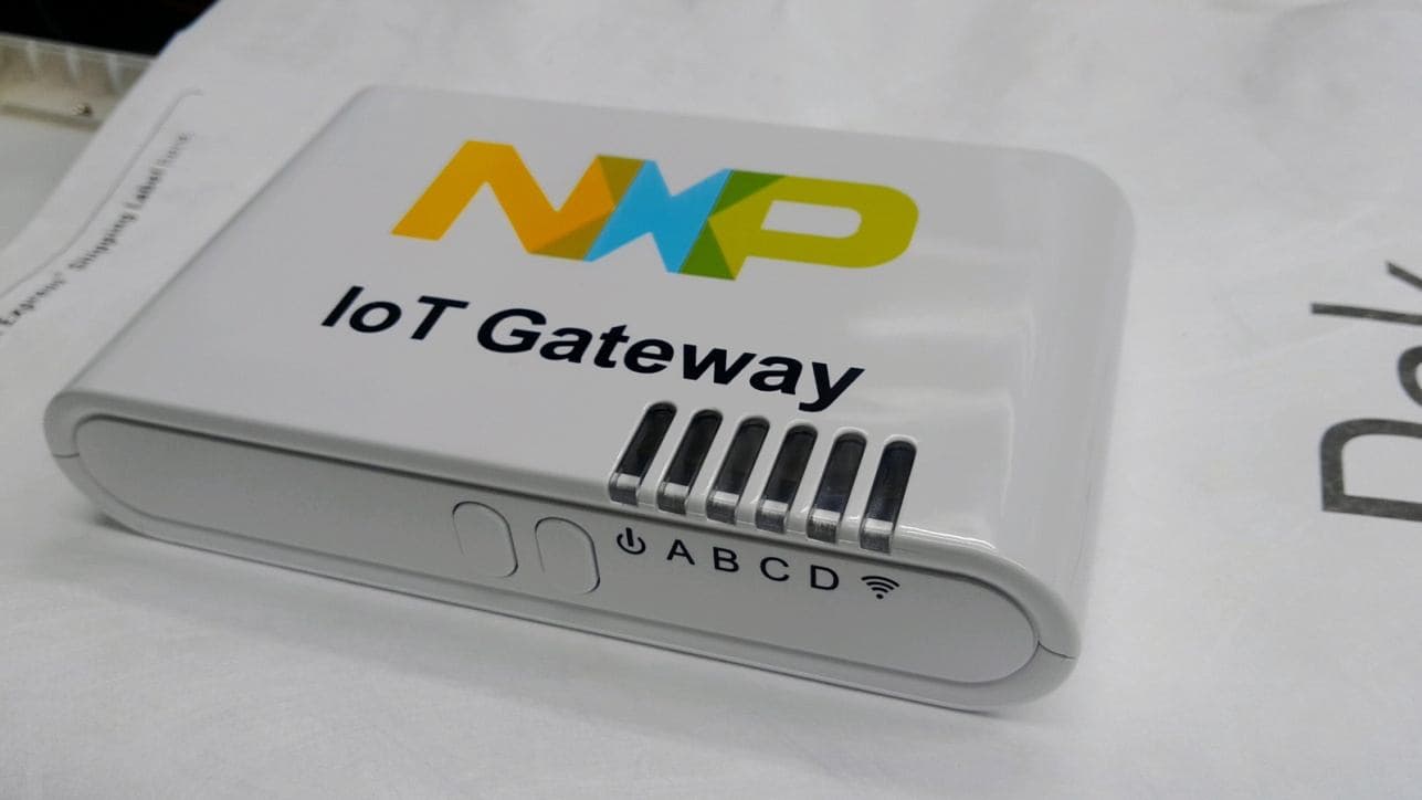
TYOJN5168IT00
Oct 22, 2013JN5168-RD6040-IoT Gateway
Equipment Class
DTS - Digital Transmission System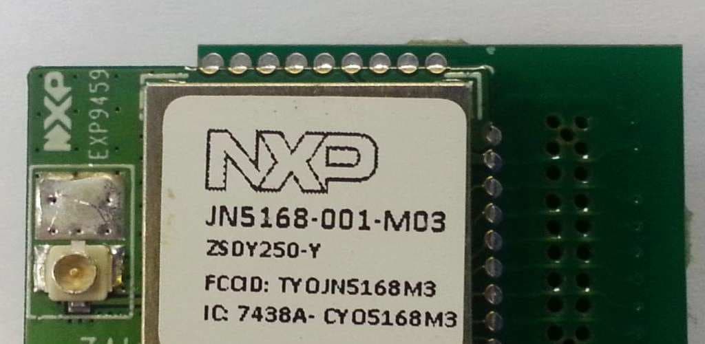
TYOJN5168M3
Jan 08, 2013JN5168-��1-M�3 IEEE802.15.4 Wireless Module
Equipment Class
DTS - Digital Transmission System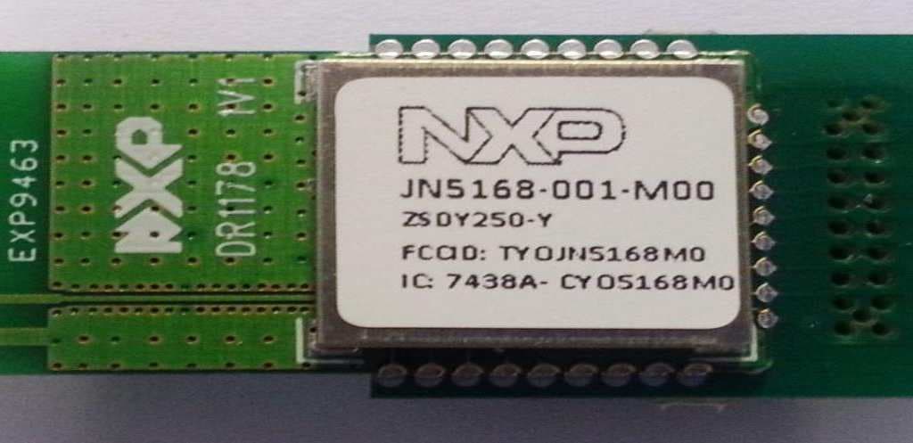
TYOJN5168M0
Jan 08, 2013JN5168-��1-M�� IEEE802.15.4 Wireless Module
Equipment Class
DTS - Digital Transmission System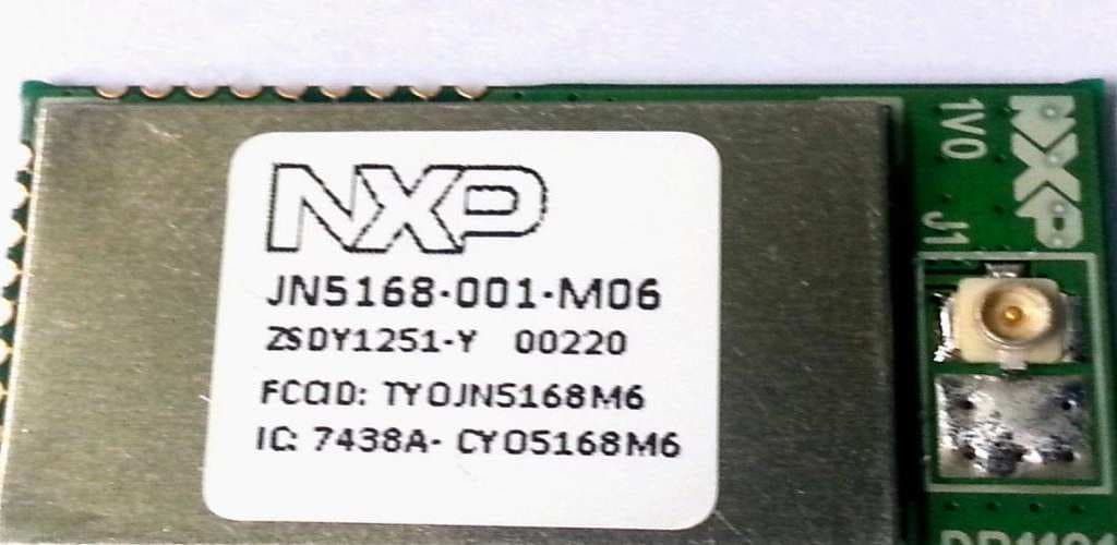
TYOJN5168M6
Jan 03, 2013JN5168-001-M�6 IEEE802.15.4 Wireless Module
Equipment Class
DTS - Digital Transmission System
TYOJN5168M5
Jan 03, 2013JN5168-001-M�5 IEEE802.15.4 Wireless Module
Equipment Class
DTS - Digital Transmission System