TYOJN5148M6JN5148-001-M06 IEEE802.15.4 Wireless Module
NXP Laboratories UK Ltd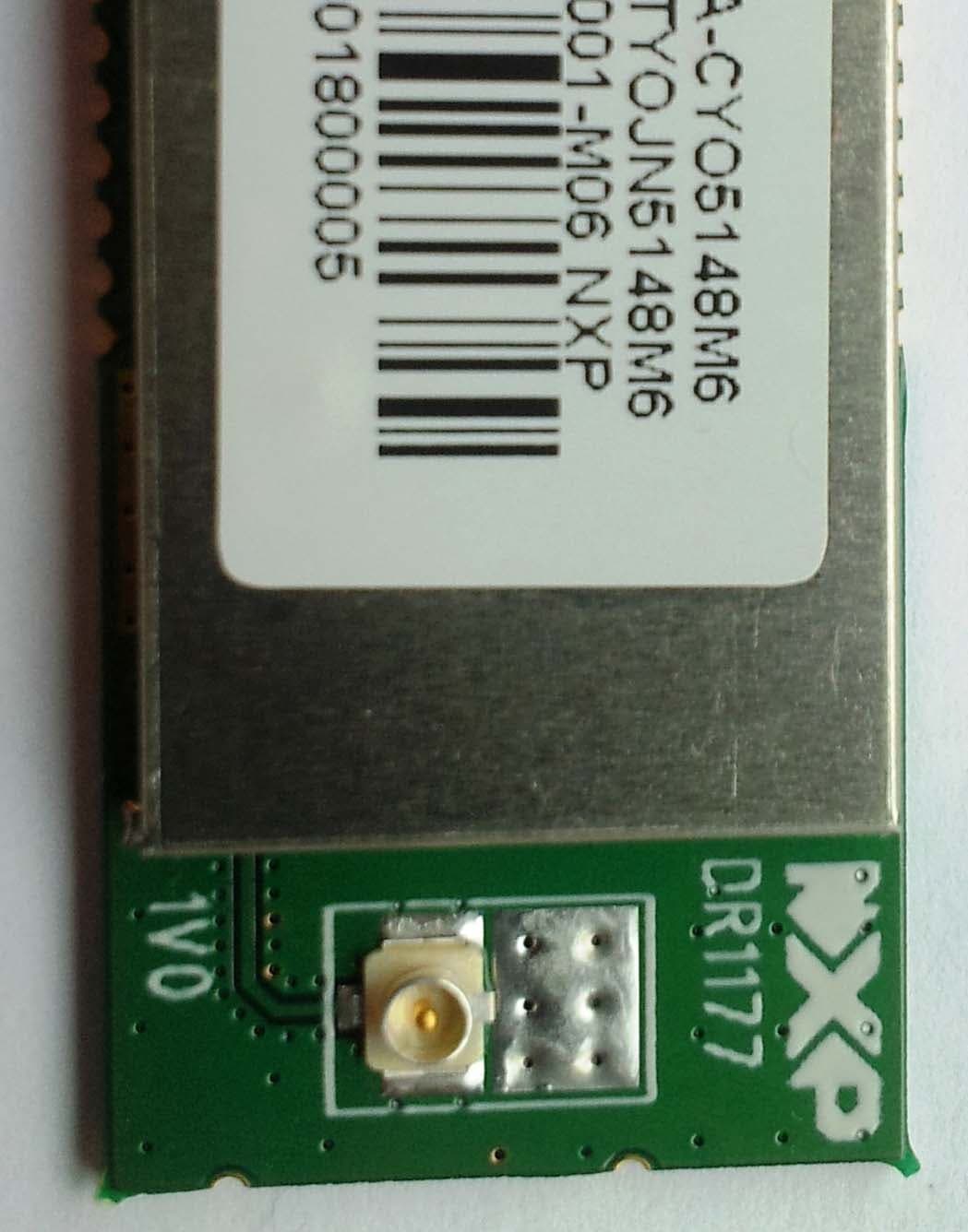
Click to zoom
Application Details
- Equipment Class
- DTS - Digital Transmission System
- Date of Grant
- Mar 20, 2012
- Application Purpose
- Original Equipment
- Date of Application
- Mar 20, 2012
- Equipment Note
- JN5148-001-M06 IEEE802.15.4 Wireless Module
- Frequency Range
- 2405.86250000 - 2479.13750000
- Company
- NXP Laboratories UK Ltd
- Country
- United Kingdom
Documents & Files
Document Text
Text extracted from the exhibit documents filed with the FCC. Open a document above to read the original.
Users Manual
Data Sheet: JN5148-001-Myy JenNet, ZigBee PRO and IEEE802.15.4 Module JN-DS-JN5148-001-Myy 1v5 © NXP Laboratories UK 2012 Features: Module • 2.4GHz IEEE802.15.4, JenNet and ZigBee PRO compatible • JN5148-001-M00/03 up to 1km range (Ext antenna) M00: integral antenna 18x32mm M03: uFl connector 18x30mm o TX power +2.5dBm o Receiver sensitivity –95dBm o TX current 15mA o RX current 17.5mA o 2.3-3.6V operation • JN5148-001-M06 up to 4km range (Ext Antenna) o 22dBm TX Power o 18dBm TX power (M04 compatible) o Receiver sensitivity -100dBm o uFl connector o TX current 84mA o RX current 23mA o 18x41mm o 2.3-3.6V operation Features: Microcontroller • 32-bit RISC CPU, up to 32MIPs with low power • 128kB ROM stores system code • 128kB RAM stores system data and bootloaded program code • 4Mbit serial flash for program code and data • On chip OTP efuse • JTAG debug interface • 4-input 12-bit ADC, 2 12-bit DACs, 2 comparators • 3 application timer/counters, • 2 UARTs • SPI port with 5 selects • 2-wire serial interface • 4-wire digital audio interface • Watchdog timer • Up to 21 DIO Industrial temp (-40°C to +85°C) Lead-free and RoHS compliant Overview The JN5148-001-Myy family is a range of ultra low power, high performance surface mount modules targeted at JenNet and ZigBee PRO networking applications, enabling users to realise products with minimum time to market and at the lowest cost. They remove the need for expensive and lengthy development of custom RF board designs and test suites. The modules use NXP’s JN5148 wireless microcontroller to provide a comprehensive solution with large memory, high CPU and radio performance and all RF components included. All that is required to develop and manufacture wireless control or sensing products is to connect a power supply and peripherals such as switches, actuators and sensors, considerably simplifying product development. Three module variants are available: JN5148-001-M00 with an integrated antenna, JN5148-001-M03 with an antenna connector and the JN5148-001-M06 with an antenna connector, power amplifier and LNA for extended range. The modules can implement networking stacks such as JenNet and ZigBee PRO, as well as customer applications Module Block Diagram Benefits • Microminiature module solutions • Ready to use in products • Minimises product development time • No RF test required for systems • Compliant with FCC part 15 rules, IC Canada RSS 210e, ETSI EN 300-328 Applications • Robust and secure low power wireless applications • ZigBee PRO and JenNet networks • Home and commercial building automation • Utilities metering (e.g. AMR) • Location Aware services (e.g. Asset Tracking) • Toys and gaming peripherals • Industrial systems • Telemetry • Remote Control Timers UARTs 12-bit ADC, comparators 12-bit DACs, temp sensor 2-wire serial SPI RAM 128kB 128-bit AES Encryption Accelerator 2.4GHz Radio ROM 128kB RISC CPU Power Management XTAL O-QPSK Modem IEEE802.15.4 MAC Accelerator 512kB Serial Flash Memory JN5148 chip Power Matching uFl Connector Matching Integrated Antenna Matching uFl Connector PA / LNA External Antenna M00 Option M03 Option M06 Option 4-Wire Audio Sleep Counters 32-byte OTP eFuse Watchdog timer Time of Flight Engine ii JN-DS-JN5148-001-Myy 1v5 © NXP Laboratories UK 2012 Contents 1. Introduction 3 1.1. Variants 3 1.2. Regulatory Approvals 3 2. Specifications 4 3. Product Development 6 3.1. JN5148 Single Chip Wireless Microcontroller 6 4. Pin Configurations 7 4.1. Pin Assignment 8 4.2. Pin Descriptions 9 4.2.1 Power Supplies 9 4.2.2 SPI Memory Connections 9 5. Electrical Characteristics 10 5.1. Maximum Ratings 10 5.2. Operating Conditions 10 Appendix A Additional Information 11 A.1 Outline Drawing 11 A.2 Module PCB Footprint 14 A.3 Manufacturing 15 A.3.1 Reflow Profile 15 A.3.2 Soldering Paste and Cleaning 15 A.4 Ordering Information 16 A.5 Tape and Reel Information: 17 A.5.1 Tape Orientation and dimensions 17 A.5.2 Cover tape details 17 A.5.3 Leader and Trailer 18 A.5.4 Reel Dimensions: 18 A.6 Related Documents 18 A.7 Federal Communication Commission Interference Statement 19 A.7.1 Antennas approved by FCC for use with JN5148 modules 20 A.7.2 High Power Module usage limitation 20 A.7.3 FCC End Product Labelling 20 A.8 Industry Canada Statement 21 A.8.1 Industry Canada End Product Labelling 21 A.9 European R & TTE Directive 1999/5/EC Statement 21 A.10 RoHS Compliance 22 A.11 Status Information 22 A.12 Disclaimers 22 Version Control 23 © NXP Laboratories UK 2012 JN-DS-JN5148-001-Myy 1v5 3 1. Introduction The JN5148-001-Myy module family provides designers with a ready made component that provides a fully integrated solution for applications, using the IEEE802.15.4 standard in the 2.4-2.5GHz ISM frequency band [1], including JenNet and ZigBee PRO, and can be quickly and easily included in product designs. The modules integrate all of the RF components required, removing the need to perform expensive RF design and test. Products can be designed by simply connecting sensors and switches to the module IO pins. The modules use NXP’s single chip IEEE802.15.4 Wireless Microcontroller, allowing designers to make use of the extensive chip development support material. Hence, this range of modules allows designers to bring wireless applications to market in the minimum time with significantly reduced development effort and cost. Three variants are available: JN5148-001-M00 (standard module with integral antenna), JN5148-001-M03 (standard module with uFl connector for use with external antennae) and JN5148-001-M06 (high RF power with uFL connector, improved sensitivity module for evaluation of extended range applications). All modules have FCC modular approvals, CE approval and are compliant with EU regulations. The variants available are described below. 1.1. Variants 1.2. Regulatory Approvals All module types have been tested against the requirements of the following European standards. For the Radio, EN 300 328 v1.7.1. EMC, EN 301 489-17 v2.1.1 …
Text truncated - open the document above for the full version.
Attestation Statements
TRaC Global 100 Frobisher Business Park, Leigh Sinton Road Malvern, Worcestershire, WR14 1BX, UK Date 7 th March, 2012 Letter of Agency To Whom It May Concern: We certify that we are not subject to denial of federal benefits that includes FCC benefits, pursuant to Section 5301 of the Anti-Drug Abuse ACT of 1988, U.S.C. 862. Further, no party, as defined in 47 CFR 1.2002(b), to the application, is subject to denial of federal benefits, that includes FCC benefits. Thank you for your attention to these matters. Yours faithfully Full Name Mr Conrad V Farlow NXP Laboratories (UK) Ltd
Block Diagram
1.1 Radio Figure 1 shows the single ended radio architecture. LNA synth PA ADC Reference & Bias Switch Radio Calibration Lim1Lim2Lim3Lim4 sigma delta D-Type Figure 1: Radio Architecture The radio comprises a low-IF receive path and a direct modulation transmit path, which converge at the TX/RX switch. The switch connects to the external single ended matching network, which consists of two inductors and a capacitor, this arrangement creates a 50 Ω port and removes the need for a balun. A 50Ω single ended antenna can be connected directly to this port. The 32MHz crystal oscillator feeds a divider, which provides the frequency synthesiser with a reference frequency. The synthesiser contains programmable feedback dividers, phase detector, charge pump and internal Voltage Controlled Oscillator (VCO). The VCO has no external components, and includes calibration circuitry to compensate for differences in internal component values due to process and temperature variations. The VCO is controlled by a Phase Locked Loop (PLL) that has an internal loop filter. A programmable charge pump is also used to tune the loop characteristic. The receiver chain starts with the low noise amplifier / mixer combination whose outputs are passed to a lowpass filter, which provides the channel definition. The signal is then passed to a series of amplifier blocks forming a limiting strip. The signal is converted to a digital signal before being passed to the Modem. The gain control for the RX path is derived in the automatic gain control (AGC) block within the Modem, which samples the signal level at various points down the RX chain. To improve the performance and reduce current consumption, automatic calibration is applied to various blocks in the RX path. In the transmit direction, the digital stream from the Modem is passed to a digital sigma-delta modulator which controls the feedback dividers in the synthesiser, (dual point modulation). The VCO frequency now tracks the applied modulation. The 2.4 GHz signal from the VCO is then passed to the RF Power Amplifier (PA), whose power control can be selected from one of three settings. The output of the PA drives the antenna via the RX/TX switch
Cover Letter(s)
NXP Laboratories (UK) Ltd, Furnival Street, Sheffield, South Yorkshire, S1 4QT, UK Tel: +00 44 114 281 2655, Fax: +00 44 114 281 2951, www.nxp.com TRaC Global 100 Frobisher Business Park, Leigh Sinton Road Malvern, Worcestershire, WR14 1BX, UK Date 15 th March, 2012 RE: TYOJN5148M6 - JN5148 Silicon variants To whomever it may concern. The below statements are made by NXP Laboratories (UK) Ltd in support of the FCC request for modular approval: List of Variants Table 1 below lists the JN5148 silicon variants all of which utilise an identical radio. The ROM stacks reside above the PHY layer and cannot affect the radio parameters in any way. Variant Stacks (ROM) Radio (Project name) Comments JN5148-001 Peripheral API, MAC2003 JN5148-T01 JN5148-J01 Peripheral API, MAC 2003/2006, Jennet V1.5, 6LOWPAN Has some software features of T01 disabled by an e-fuse bit JN5148-Z01 Peripheral API, MAC 2003/2006, Zigbee PRO JAGUAR Table 1: JN5148 Silicon variants Please note that some of these variants are only available to specific customers and do not appear on either the module user guide or the chip datasheet. Yours Sincerely Conrad V Farlow NXP Laboratories (UK) Ltd
ID Label/Location Info
TYOJN5148M6 Module Labelling This document has been generated in support of the FCCID application for the TYOJN5148M6 module. It covers the following products: JN5148-ØØ1-MØ6, JN5148-JØ1-MØ6, JN5148-TØ1-MØ6 and JN5148-ZØ1-MØ6 as detailed on the silicon summary cover letter. The following picture shows an example of NXP’s module labelling. The location, on top of the metal screening can, is also demonstrated. JN5148-001-M06 Subsequent to being granted an FCC-ID the following label will be used for JN5148- 001-M06. Product Identification Instructions Label line 1: Industry Canada ID Number Label line 2: FCC ID Number Label line 3: Part Name Label line 4: Barcode Label line 5: YYWWTNNNNN (see below) Identifier Description Format YY Year 06(example) WW Week 45(example) T Module type 7 NNNNN Serial Number FCCID: TYOJN5148M6 YYWWTNNNNN IC: 7438A-CYO5148M6 JN5148-001-M06 NXP JN5148-J01-M06 Subsequent to being granted an FCC-ID the following label will be used for JN5148- J01-M06. Product Identification Instructions Label line 1: Industry Canada ID Number Label line 2: FCC ID Number Label line 3: Part Name Label line 4: Barcode Label line 5: YYWWTNNNNN (see below) Identifier Description Format YY Year 06(example) WW Week 45(example) T Module type 7 NNNNN Serial Number JN5148-T01-M06 Subsequent to being granted an FCC-ID the following label will be used for JN5148- T01-M06. Product Identification Instructions Label line 1: Industry Canada ID Number Label line 2: FCC ID Number Label line 3: Part Name Label line 4: Barcode Label line 5: YYWWTNNNNN (see below) Identifier Description Format YY Year 06(example) WW Week 45(example) T Module type 7 NNNNN Serial Number FCCID: TYOJN5148M6 YYWWTNNNNN IC: 7438A-CYO5142M6 JN5148-J01-M06 NXP FCCID: TYOJN5148M6 YYWWTNNNNN IC: 7438A-CYO5142M6 JN5148-T01-M06 NXP JN5148-Z01-M06 Subsequent to being granted an FCC-ID the following label will be used for JN5148- Z01-M06. Product Identification Instructions Label line 1: Industry Canada ID Number Label line 2: FCC ID Number Label line 3: Part Name Label line 4: Barcode Label line 5: YYWWTNNNNN (see below) Identifier Description Format YY Year 06(example) WW Week 45(example) T Module type 7 NNNNN Serial Number FCCID: TYOJN5148M6 YYWWTNNNNN IC: 7438A-CYO5142M6 JN5148-Z01-M06 NXP
Operational Description
1.1 Radio Figure 1 shows the single ended radio architecture. LNA synth PA ADC Reference & Bias Switch Radio Calibration Lim1Lim2Lim3Lim4 sigma delta D-Type Figure 1: Radio Architecture The radio comprises a low-IF receive path and a direct modulation transmit path, which converge at the TX/RX switch. The switch connects to the external single ended matching network, which consists of two inductors and a capacitor, this arrangement creates a 50 Ω port and removes the need for a balun. A 50Ω single ended antenna can be connected directly to this port. The 32MHz crystal oscillator feeds a divider, which provides the frequency synthesiser with a reference frequency. The synthesiser contains programmable feedback dividers, phase detector, charge pump and internal Voltage Controlled Oscillator (VCO). The VCO has no external components, and includes calibration circuitry to compensate for differences in internal component values due to process and temperature variations. The VCO is controlled by a Phase Locked Loop (PLL) that has an internal loop filter. A programmable charge pump is also used to tune the loop characteristic. The receiver chain starts with the low noise amplifier / mixer combination whose outputs are passed to a lowpass filter, which provides the channel definition. The signal is then passed to a series of amplifier blocks forming a limiting strip. The signal is converted to a digital signal before being passed to the Modem. The gain control for the RX path is derived in the automatic gain control (AGC) block within the Modem, which samples the signal level at various points down the RX chain. To improve the performance and reduce current consumption, automatic calibration is applied to various blocks in the RX path. In the transmit direction, the digital stream from the Modem is passed to a digital sigma-delta modulator which controls the feedback dividers in the synthesiser, (dual point modulation). The VCO frequency now tracks the applied modulation. The 2.4 GHz signal from the VCO is then passed to the RF Power Amplifier (PA), whose power control can be selected from one of three settings. The output of the PA drives the antenna via the RX/TX switch
Parts List/Tune Up Info
Component ReferenceDescriptionManufacturerManufacturer PartSupplierSupplier PartNotes C3, C6-8, C14-17, C20Capacitor 100nF 0402 X5RBourns YageoCC0402AX5R104KTRFlintCC0402AX5R104KTR. C10,C11Capacitor 15pF 0402 COGKEMETC0402C150J5GACTUFarnell InOne1414577. C13Capacitor 10uF 6.3V 0805 X5RKEMETC0805C106K9PACFarnell InOne922-7814. C1, C9, C12, C18, C24Capacitor 47pF 0402 NPOPhyComp(Yageo)2.23887E+11Flint2238-869-15479. C4, C21Capacitor 1pF 0402 NPOMurataGRM1555C1H1R0CZ01DFarnell InOne8819530. C5, C19Capacitor 10pF 0402 NPOPhyComp(Yageo)2238 869 15109Farnell InOne3019-160. C2Capacitor 10nF 0402 X7RPhyComp(Yageo)2.23879E+11Farnell InOne301-9275. C22Capacitor 1.2pF 0402 NPOmuRataGRM1555C1H1R2CZ01DDigiKey490-1265-1-ND. J1UFL ConnectorHiroseCL331-0471-0-10HiroseCL331-0471-0-10. L1Inductor 5.6nHmuRataLQP15MN5N6B02Farnell InOne1515368. L2Inductor 2n4H muRataLQP15MN2N4B02DigiKeyLQP15MN2N4B02D-ND. L3Inductor 2.7nH muRataLQP15MN2N7B02Farnell InOne1404732. L4Inductor 5.1nHmuRataLQP15MN5N1B02Farnell InOne1515367. Q1Transistor, N Channel MOSFET, BSH103NXPBSH103Farnell InOne1081307. R1Resistor 43K 0402 1%PhyComp(Yageo)2.32271E+11Farnell InOne145-8795 . R2Resistor 1K2_0402 1%PhyComp(Yageo) RC0402FR-071K2LFarnell InOne9239243. R3Resistor 1K5 0402 1%PhyComp(Yageo)RC0402FR-071K5LFarnell InOne9239251. R4Resistor 47K 0402 1%PhyComp(Yageo)RC0402FR-0747KLFarnell InOne9239430. U1IC JN5148NXPJN5148-001, JN5148-J01, JN5148-T01, JN5148-Z01NXPJN5148-001. U2IC Serial 3V Flash SMD M25P40-AVMN6PBNumonyxM25P40-VMN6PBFarnell InOne988-2871 . U4-574AHC1G32NXP74AHC1G32GW/T1Farnell InOne1085242. U6SE2431LSkyworksSE2431LSiGe SemiconductorSE2431L. Y1Crystal SMD 32 MHzAELX32M000000S039AAELX32M000000S039A. AssemblyDescription DR1177JN5148 HP uFL Module
RF Exposure Info
Prediction of Distance for a specific MPE Limit Equation from page 18 of OET Bulletin 65, Edition 97-01 S = power density P = power input to the antenna G = power gain of the antenna in the direction of interest relative to an isotropic radiator R = distance to the centre of radiation of the antenna Max input to antenna terminal 23 dBm 199.53 Max Antenna gain 2.2 dBi 1.67 Prediction Freq 2.405 GHz 2.405E+09 MPE limit for uncontrolled exposure at prediction frequency 1 mW/cm 2 Permitted distance at MPE limit (1 mW/cm2) in cm 5.15* Application is for a mobile device manufacturer is recommending 20cm min distance. S PG R π4 = 2 4R PG S π =
Schematics
1V0 11/11/2011 11/11/2011 MDG CF NXP JN5148 HP uFL Module C DR1177 Not to Scale 1 2 REV: SIZE: CODE: DRAWN: DATED: DATED: CHECKED: QUALITY CONTROL: DATED: DATED: RELEASED: COMPANY: TITLE: DRAWING NO: SHEET: OF SCALE: REVISION RECORD APPROVED: ECO NO: LTR DATE: 1 2 3 4 5 6 D C B A C D B A RF IN/OUT JN5148 Reference Design Can Pads Flash Memory 32MHz Crystal 1 2 C11 15pF 0402C_JENNIC 1 2 C10 15pF 0402C_JENNIC 1 2 R1 43k 0402C_JENNIC 1 2 L1 5n6H 1 2 C1 47pF 0402C_JENNIC 1 2 L2 2n4H 1 2 C6 100nF 0402C_JENNIC 1 2 C7 100nF 0402C_JENNIC 1 2 C18 47pF 0402C_JENNIC 1 2 C15 100nF 0402C_JENNIC 1 2 C24 47pF 0402C_JENNIC 1 2 C2 10nF 0402C_JENNIC 1 2 C3 100nF 0402C_JENNIC 1 2 C12 47pF 0402C_JENNIC 1 2 C20 100nF 0402C_JENNIC 6 CLK 5 SDI 3 WP 1 SS 7 HOLD 2 SDO 8 VCC 4 VSS U2 M25PX0_SO8_JENNIC 2 1 C14 100nF 0402C_JENNIC 2 1 C16 100nF 0402C_JENNIC EC22 EC23 EC27 EC28 EC30 EC31 EC32 EC33 EC34 EC35 EC36 EC10 EC11 EC12 EC15 EC16 EC17 EC18 EC19 EC20 EC21 EC29 EC24 EC25 EC26 EC6 EC8 EC7 EC14 EC13 EC9 1 X1 2 GND 4 GND 3 X2 Y1 TSX-3225_JENNIC EC37 EC38 EC5 EC4 EC41 EC40 EC39 EC1 EC2 EC3 1 DIO16 2 DIO17 3 TEST_EN 4 DIO18 5 DIO19 6 VSS2 7 VSSS 8 XTAL_OUT 9 XTAL_IN 10 VB_SYNTH 11 VCOTUNE 12 VB_VCO 13 VDD1 14 IBIAS 15 VREF 16 VB_RF2 17 RF_IN 18 VB_RF 19 COMP1M/EXT_PA_B 20 COMP1P/EXT_PA_C 21 ADC1 22 ADC2 23 ADC3 24 ADC4 25 COMP2M 26 COMP2P 27 VB_A 28 NC 29 DAC1 31 DIO20 30 DAC2 32 VSS1 33 SPICLK 34 SPIMISO 35 VB_RAM 36 SPIMOSI 37 SPISEL0 38 DIO0 39 RESETN 40 VB_DIG 41 DIO1 42 DIO2 43 DIO3 44 DIO4 45 DIO5 46 DIO6 47 DIO7 48 DIO8 49 VDD2 50 DIO9 51 DIO10 52 DIO11 53 DIO12 54 DIO13 55 DIO14 56 DIO15 57 VSSA U1 JN5148_JENNIC 1 2 C9 47pF 0402C_JENNIC 1 2 C8 100nF 0402C_JENNIC 1 TP3 TPTINY 2 1 C13 10uF 0805C_JENNIC EC42 EC43 EC44 Q1 1 TP43 TP 1 TP44 TP 1 TP45 TP 1 TP46 TP EC45 X2 VB_RAM VB_DIG VB_SYNTH VB_VCO VB_RF VREF IBIAS X1 SWP VCC VCC SSM SPIMOSI SPICLK SPIMISO VB_RF VCC DIO19 DIO18 DIO17 DIO16 DIO15 DIO14 DIO13 DIO12 DIO11 DIO10 DIO9 DIO8 DIO7 DIO6 DIO5 DIO4 DIO1 DIO0 DIO[0:20] SSZ SSM SWP SPIMISO SPIMOSI SPICLK VCC RESETN IBIAS VREF VB_RF X1 X2 DIO2 DIO3 DIO4 DIO5 DIO6 DIO7 DIO10 DIO11 DIO12 DIO13 DIO14 DIO16 DIO17 DIO18 DIO19 C1M C1P ADC1 ADC2 ADC3 ADC4 C2M C2P VB_A C1M C1P C2M C2P ADC3 ADC2 ADC1 ADC4 DAC1 DAC2 VB_A DAC1 VB_SYNTH VB_VCO DIO20 DIO8 DIO15 DIO20 DIO0 SPIMISO SSZ RESETN DAC2 DIO1 DIO9 SPIMOSI SPICLK VB_DIG VB_RAM RF_PORT NC VB_DIG VREF 1V0 11/11/2011 11/11/2011 DR1177 Not to Scale CF MDG JN5148 HP uFL Module NXP C 2 2 REV: SIZE: CODE: DRAWN: DATED: DATED: CHECKED: QUALITY CONTROL: DATED: DATED: RELEASED: COMPANY: TITLE: DRAWING NO: SHEET: OF SCALE: REVISION RECORD APPROVED: ECO NO: LTR DATE: 1 2 3 4 5 6 D C B A C D B A FEM Logic 1 2 3 4 J1 UFL_SM_JENNIC 1 B2 2 B1 3 NC 4 NC 5 VCC 6 TX/RX 7 NC 19 VCC 18 GND 17 NC 16 ANT_SEL 15 ANT1 14 GND 13 ANT2 20 CSD 21 CPS 22 VCC 23 BOUT 24 CTX 25 GND 12 GND 11 GND 10 GND 9 GND 8 NC U6 SE2431L_JENNIC 1 2 R2 1K2 1 2 R3 1K5 1 2 C5 10pF 1 2 C17 100nF 1 2 C19 10pF 1 2 4 U4 74HC1G32_JENNIC 1 2 4 U5 74HC1G32_JENNIC 1 2 C4 1pF 1 2 C21 1pF 1 2 L3 2.7nH 1 2 R4 47K 1 2 C22 1p2F 1 2 L4 5n1H RF_PORT DIO3 VCC CSD CPS DIO2 DIO3 CSD NC DIO3 CPS VCC
Test Report
File nameNXPLABSUK.4933-3PAGE 1 OF 69 QMF21J – 3: FCC PART 15C: RNE ISSUE 02: - JUN 10 FCC 47CFR part 15C Test Report For 2.4GHz IEEE 802.15.4 wireless controller module JN5148-001-M06 Reference Standard: FCC 47CFR part 15C Manufacturer: NXP Labs UK Ltd For type of equipment and serial number, refer to section 3 Report Number: 01-540/4933/3/12 Report Produced by: -R.N. Electronics Ltd. 1 Arnolds Court Arnolds Farm Lane Mountnessing Essex CM13 1UT U.K. www.RNelectronics.comTelephone +44 (0) 1277 352219 Facsimile +44 (0) 1277 352968 2004RN ELECTRONICS LIMITEDREPORT NUMBER 01-540/4933/3/12 ALL RIGHTS RESERVED File nameNXPLABSUK.4933-3PAGE 2 OF 69 QMF21J – 3: FCC PART 15C: RNE ISSUE 02: - JUN 10 1.Contents 1.CONTENTS............................................................................................................................................. 2 2.SUMMARY OFTESTRESULTS.................................................................................................................. 3 3.EQUIPMENTUNDERTEST(EUT)............................................................................................................. 4 3.1Equipment Specification....................................................................................... 4 3.2EUT Configurations for testing ............................................................................. 4 3.3EUT Modes.......................................................................................................... 4 3.4Emissions Configuration ...................................................................................... 6 4.SPECIFICATIONS.................................................................................................................................... 7 4.1Deviations ........................................................................................................... 7 4.2Tests at Extremes of Temperature & Voltage ....................................................... 7 4.3Measurement Uncertainties ................................................................................. 7 5.TESTS,METHODS ANDRESULTS............................................................................................................. 8 5.1Conducted Emissions .......................................................................................... 8 5.2Radiated Emissions ............................................................................................. 9 5.3Intentional Radiator Field Strength/Peak Conducted Power ............................... 10 5.4Duty Cycle ......................................................................................................... 12 5.5Maximum Spectral Power Density...................................................................... 13 5.66 Bandwidth....................................................................................................... 14 5.7Band Edge Compliance...................................................................................... 15 6.PLOTS ANDRESULTS............................................................................................................................17 6.1Conducted Emissions ........................................................................................ 17 6.2Radiated Emissions ........................................................................................... 18 6.3Fundamental Emissions ..................................................................................... 44 6.4Duty Cycle ......................................................................................................... 47 6.56dB Bandwidth................................................................................................... 48 6.6Band Edge Compliance...................................................................................... 50 6.7Spectral Density ................................................................................................ 57 7Explanatory Notes ................................................................................................. 59 7.1Explanation of FAIL LIMIT 1 Statement .............................................................. 59 7.2Explanation of limit line calculations for radiated measurements......................... 59 8.PHOTOGRAPHS.....................................................................................................................................60 IDENTIFYINGPHOTOGRAPHS OF THEEUT ......................................................................................................62 9.SIGNALLEADS.....................................................................................................................................63 10.TESTEQUIPMENTCALIBRATION LIST..................................................................................................64 11.AUXILIARY EQUIPMENT......................................................................................................................65 11.1Auxiliary equipment supplied by NXP Laboratories UK Ltd.............................. 65 11.2Auxiliary equipment supplied by RN Electronics Limited.................................. 65 12.MODIFICATIONS................................................................................................................................66 12.1Modifications before test ................................................................................ 66 12.2Modifications during test................................................................................. 66 13.Compliance information ...................................................................................... 67 14DESCRIPTION OFTESTSITES............................................................................................................68 15ABBREVIATIONS ANDUNITS...............................................................................................................69 2004RN ELE…
Text truncated - open the document above for the full version.
Contact Information
Applicant
Conrad Farlow
Test Firm
R.N. Electronics Ltd.Roger Ray
Technical Specifications
| # | Rule Parts | Frequency Range | Power Output |
|---|---|---|---|
| 1 | 15C | 2.41 GHz - 2.48 GHz | 104.70 mW |
Other Applications from NXP Laboratories UK Ltd
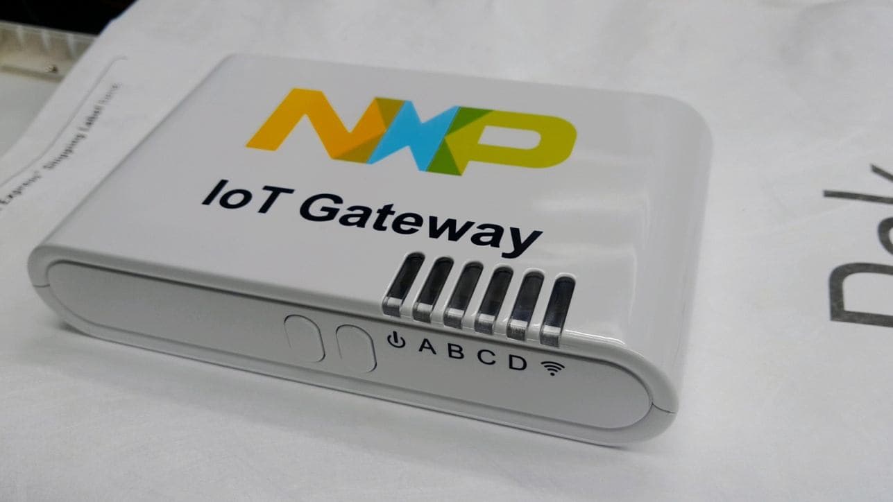
TYOJN5168IT00
Oct 22, 2013JN5168-RD6040-IoT Gateway
Equipment Class
DTS - Digital Transmission System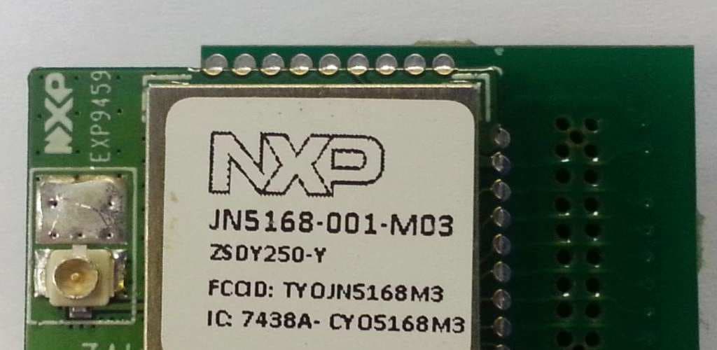
TYOJN5168M3
Jan 08, 2013JN5168-��1-M�3 IEEE802.15.4 Wireless Module
Equipment Class
DTS - Digital Transmission System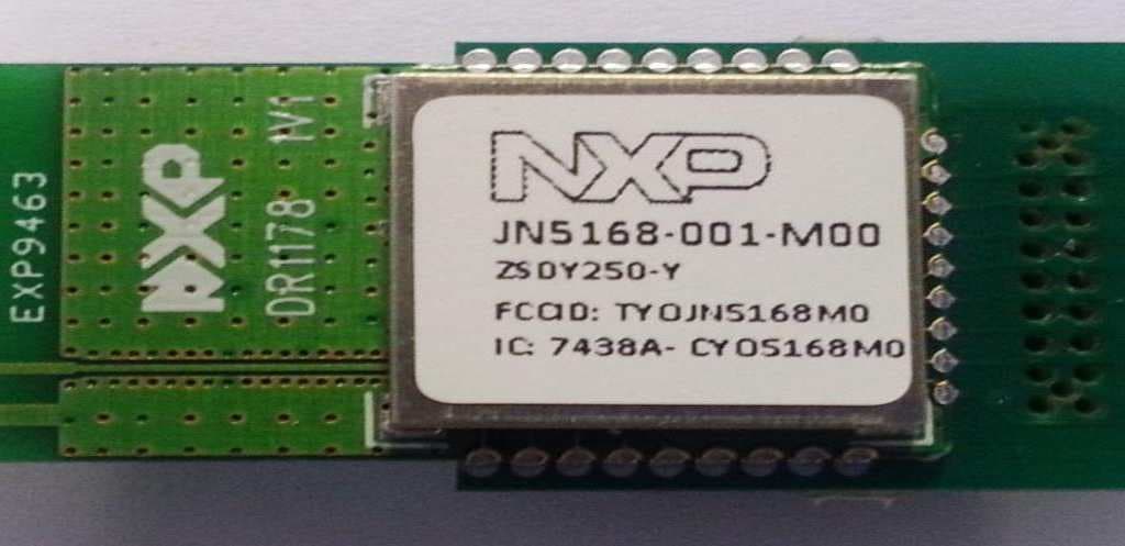
TYOJN5168M0
Jan 08, 2013JN5168-��1-M�� IEEE802.15.4 Wireless Module
Equipment Class
DTS - Digital Transmission System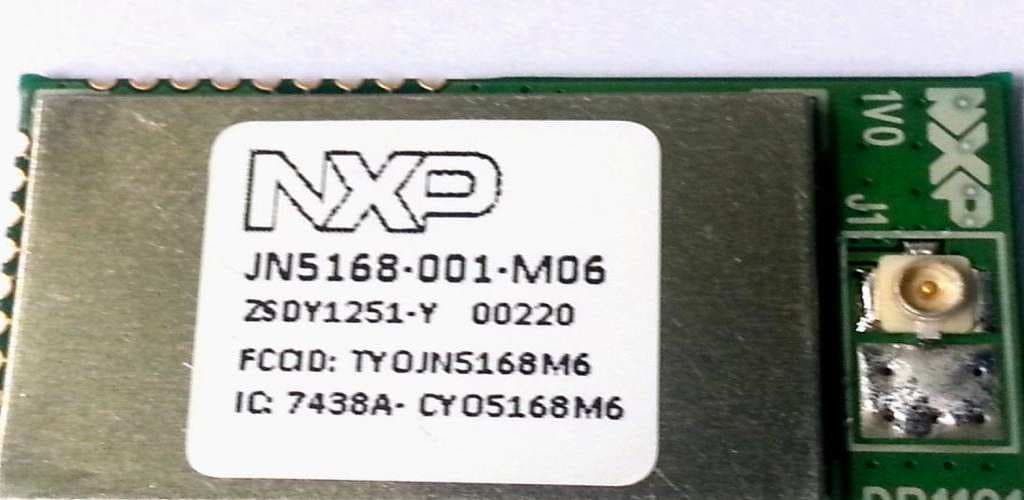
TYOJN5168M6
Jan 03, 2013JN5168-001-M�6 IEEE802.15.4 Wireless Module
Equipment Class
DTS - Digital Transmission System
TYOJN5168M5
Jan 03, 2013JN5168-001-M�5 IEEE802.15.4 Wireless Module
Equipment Class
DTS - Digital Transmission System