TYOJN5148U0JN5148 IEEE802.15.4 USB Dongle
NXP Laboratories UK Ltd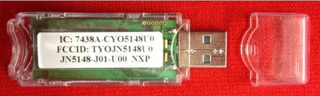
Click to zoom
Application Details
- Equipment Class
- DTS - Digital Transmission System
- Date of Grant
- Oct 08, 2012
- Application Purpose
- Original Equipment
- Date of Application
- Oct 08, 2012
- Equipment Note
- JN5148 IEEE802.15.4 USB Dongle
- Frequency Range
- 2405.00000000 - 2480.00000000
- Company
- NXP Laboratories UK Ltd
- Country
- United Kingdom
Documents & Files
Document Text
Text extracted from the exhibit documents filed with the FCC. Open a document above to read the original.
Users Manual
JN5148 High-Power USB Dongle (DR1131) Reference Manual JN-RM-2064 Revision 1.0 25-Jul-2012 JN5148 High-Power USB Dongle (DR1131) Reference Manual 2 © NXP Laboratories UK 2012 JN-RM-2064 v1.0 Contents About this Manual 3 Organisation 3 Conventions 3 Acronyms and Abbreviations 3 Related Documents 3 1 Introduction 4 1.1 Features 4 1.2 Reference Design 4 2 Hardware Overview 5 2.1 Dongle Layout 5 2.2 LPC1343 Device 5 2.3 JN5148 Device 5 2.4 High-Power Front-End 6 2.5 LNA Bypass 6 2.6 LEDs 6 3 Programming the LPC1343 Device 7 4 Programming the JN5148 Device 8 4.1 Re-programming USB Dongles 8 4.2 Preparing the Binary File 8 4.3 Programming the Dongle 8 4.4 Installing Device Driver for USB Dongle 9 JN5148 High-Power USB Dongle (DR1131) Reference Manual JN-RM-2064 v1.0 © NXP Laboratories UK 2012 3 About this Manual This manual provides a detailed reference for NXP’s JN5148 High-Power USB Dongle (DR1131). The manual is part of the reference design JN-RD-6034. Organisation This manual consists of 4 chapters, as follows: Chapter 1 outlines the features and functions of the USB dongle Chapter 2 provides detailed feature information Chapter 3 describes programming the LPC1343 device on the dongle Chapter 4 describes programming the JN5148 device on the dongle Conventions Files, folders, functions and parameter types are represented in bold type. Function parameters are represented in italics type. Code fragments are represented in the Courier typeface. Acronyms and Abbreviations BOM Bill Of Materials DIO Digital Input/Output LNA Low-Noise Amplifier PCB Printed Circuit Board SDK Software Developer’s Kit UART Universal Asynchronous Receiver/Transmitter USB Universal Serial Bus Related Documents JN-DS-JN5148 JN5148 Data Sheet JN5148 High-Power USB Dongle (DR1131) Reference Manual 4 © NXP Laboratories UK 2012 JN-RM-2064 v1.0 1 Introduction This manual provides a detailed reference for the JN5148 High-Power USB Dongle, of type DR1131, supplied with JenNet-IP EK040 evaluation kit. The dongle provides a platform for hardware development environment for wireless microcontroller applications with a USB interface. 1.1 Features The dongle has the following features: JN5148-J01 device (mounted directly on the board) Integrated PCB antenna High-power capability NXP LPC1343 USB interface and connector (interface chip is connected to UART0 of the JN5148-J01 device) Two LEDs (one red and one green) This dongle is a high-power device with a radio transmission capability similar to the high-power modules provided in the JenNet-IP EK040 evaluation kit. 1.2 Reference Design A reference design (JN-RD-6034) for the JN5148 High-Power USB Dongle is available from www.nxp.com/jennic/support. The reference design comprises a ZIP file containing the following files: This Reference Manual The schematic diagram for the board The BOM (Bill Of Materials) for the board Gerbers for the board JN5148 High-Power USB Dongle (DR1131) Reference Manual JN-RM-2064 v1.0 © NXP Laboratories UK 2012 5 2 Hardware Overview 2.1 Dongle Layout 1 9 m m 45mm USB JN5148 LEDS HP Front End LPC1343 Antenna SPI Flash LPC1343 Config Connector Figure 1: DR1131 Board Layout 2.2 Dongle Block Diagram Timers UART 12-bit ADC, comparators 12-bit DACs, temp sensor SPI RAM 128kB 128-bit AES Encryption Accelerator 2.4GHz Radio ROM 128kB RISC CPU Power Management XTAL 32.768 kHz O-QPSK Modem IEEE802.15.4 MAC Accelerator 512kB Serial Flash Memory JN5148 chip Integrated Antenna 32kHz ext Xtal Sleep Counters 32-byte OTP eFuse Watchdog timer Time of Flight Engine USB LPC1343 Micro XTAL 32 MHz XTAL 12 MHz SE2431L Matching 2.3 LPC1343 Device The LPC1343 device is connected to the USB connector and acts as an interface between the PC and the JN5148 device. The LPC1343 will enumerate on the PC as two devices: 1. A mass storage device used to program the Flash device for the JN5148 2. A virtual COM port connected directly to UART0 on the JN5148 2.4 JN5148 Device The JN5148 circuit is based around the standard JN5148 reference design. JN5148 High-Power USB Dongle (DR1131) Reference Manual 6 © NXP Laboratories UK 2012 JN-RM-2064 v1.0 2.5 High-Power Front-End The front-end is a Skyworks SE2431L. This means that the dongle can achieve 22dBm output power and Rx sensitivity of -100dBm. The output of the front-end is connected to a printed antenna. 2.6 LNA Bypass If the dongle is used in the presence of very strong signals, such as Wi-Fi, then there will be a performance improvement by switching off the Low-Noise Amplifier (LNA) in the front-end to stop the input stage of the JN5148 device from being overloaded with other signals. The LNA can be bypassed using DIO1 - driving DIO1 low will bypass the LNA. 2.7 LEDs The two LEDs are connected back-to-back between DIOs 16 and 17. JN5148 High-Power USB Dongle (DR1131) Reference Manual JN-RM-2064 v1.0 © NXP Laboratories UK 2012 7 3 Programming the LPC1343 Device The LPC1343 device is supplied pre-programmed on all USB dongles. You should never need to reprogram the firmware in the LPC1343 device when developing applications for the JN5148 device. If you are producing new USB dongles or are developing new ways to communicate with the JN5148 device (i.e. new HID classes) then the mechanism for reprogramming the LPC1343 is as follows. 1. Insert the USB dongle into the PC with pins 2 and 6 of J4 connected together. 2. Wait up to 30 seconds. The dongle will now appear in Windows Explorer as a mass storage device with the title ‘CRP DISABLD’: 3. Rename your new binary FIRMWARE.BIN. 4. ‘Drag and drop’ or ‘copy and paste’ the new binary file onto the USB dongle. 5. Remove the USB dongle from the PC and re-insert it, this time with J4 pins 2 and 6 not connected together. Two pre-compiled binaries are available in the JN-RD-6034 reference design. These are: LPC1343_Firmware_0x10.bin: This binary should be used for devices that store their MAC address at address 0x10, such as the JN5148-J01 and JN5142-J01. LPC1343_Firmwar…
Text truncated - open the document above for the full version.
Attestation Statements
TRaC Global 100 Frobisher Business Park, Leigh Sinton Road Malvern, Worcestershire, WR14 1BX, UK Date 2 nd October, 2012 Letter of Agency To Whom It May Concern: We certify that we are not subject to denial of federal benefits that includes FCC benefits, pursuant to Section 5301 of the Anti-Drug Abuse ACT of 1988, U.S.C. 862. Further, no party, as defined in 47 CFR 1.2002(b), to the application, is subject to denial of federal benefits, that includes FCC benefits. Thank you for your attention to these matters. Yours faithfully Full Name Mr Conrad V Farlow NXP Laboratories (UK) Ltd
Block Diagram
Timers UART 12-bit ADC, comparators 12-bit DACs, temp sensor SPI RAM 128kB 128-bit AES Encryption Accelerator 2.4GHz Radio ROM 128kB RISC CPU Power Management XTAL 32.768 kHz O-QPSK Modem IEEE802.15.4 MAC Accelerator 512kB Serial Flash Memory JN5148 chip Integrated Antenna 32kHz ext Xtal Sleep Counters 32-byte OTP eFuse Watchdog timer Time of Flight Engine USB LPC1343 Micro XTAL 32 MHz XTAL 12 MHz SE2431L Matching
Cover Letter(s)
TRaC Global 100 Frobisher Business Park, Leigh Sinton Road Malvern, Worcestershire, WR14 1BX, UK October 8 th , 2012 MANUFACTURER’S LETTER IN SUPPORT OF THE APPLICATION OF DUTY CYCLE TYOJN5148U0 To Whom It May Concern: In normal operation the equipment employs pulsing at a variable rate, depending on the application. We declare a duty cycle of 10% and quotes IEEE 802.15.4: “The specifications of IEEE STD 802.15.4-2003 are tailored for applications with low power and low data rates (a maximum of 250 kb/s and down to 20kb/s). Typical applications for IEEE 802.15.4 devices are anticipated to run with low duty cycles (under 15). This will make IEEE 802.15.4 devices less likely to cause interference to other standards”. Below are the timings for a typical network scenario. Comprising: Wake up and radio calibration` = 2.000ms Initialization including Back off, CCA and Turnaround Time = 1.280ms TX 40 byte payload + preamble and length = 46 x 32uS = 1.472ms Turn Around Time = 0.192ms RX ACK = 0.352ms SLEEP = 10.000ms Total time = 15.296ms Duty cycle (1.472/15.296) x 100% = 9.623% Thank you for your attention to this matter. Yours faithfully Full Name Mr Conrad V Farlow NXP Laboratories (UK) Ltd WAKE & CALINIT.TXTATRX ACKSLEEP 2.000ms 1.280ms 1.472ms0.192ms0.352ms10.000ms
Cover Letter(s)
NXP Laboratories (UK) Ltd, Furnival Street, Sheffield, South Yorkshire, S1 4QT, UK Tel: +00 44 114 281 2655, Fax: +00 44 114 281 2951, www.nxp.com TRaC Global 100 Frobisher Business Park, Leigh Sinton Road Malvern, Worcestershire, WR14 1BX, UK Date 2 nd October, 2012 RE: TYOJN5148U0 - JN5148 Silicon variants To whomever it may concern. The below statements are made by NXP Laboratories (UK) Ltd in support of the FCC request for modular approval: List of Variants Table 1 below lists the JN5148 silicon variants all of which utilise an identical radio. The ROM stacks reside above the PHY layer and cannot affect the radio parameters in any way. Variant Stacks (ROM) Radio (Project name) Comments JN5148-001 Peripheral API, MAC2003 JAGUAR JN5148-T01 Peripheral API, MAC 2003/2006, Jennet V1.5, 6LOWPAN JN5148-J01 Has some software features of T01 disabled by an e-fuse bit JN5148-Z01 Peripheral API, MAC 2003/2006, Zigbee PRO Table 1: JN5148 Silicon variants Please note that some of these variants are only available to specific customers and do not appear on either the module user guide or the chip datasheet. Yours Sincerely Conrad V Farlow NXP Laboratories (UK) Ltd
ID Label/Location Info
TYOJN5148U0 USB Dongle Labelling This document has been generated in support of the FCCID application for the TYOJN5148UØ USB Dongle. It covers the following products: JN5148-ØØ1-MØ6, JN5148-JØ1-MØ6, JN5148-TØ1-MØ6 and JN5148-ZØ1-MØ6 as detailed on the silicon summary cover letter. The following picture shows an example of NXP’s USB Dongle labelling JN5148-001-UØØ Subsequent to being granted an FCC-ID the following label will be used for JN5148- 001-UØØ. Product Identification Instructions Label line 1: Industry Canada ID Number Label line 2: FCC ID Number Label line 3: Part Name Label line 4: Barcode Label line 5: YYWWTNNNNN (see below) Identifier Description Format YY Year 06(example) WW Week 45(example) T Module type 8 NNNNN Serial Number FCCID: TYOJN5148U0 YYWWTNNNNN IC: 7438A-CYO5148U0 JN5148-001-U00 NXP JN5148-J01-UØØ Subsequent to being granted an FCC-ID the following label will be used for JN5148- J01-UØØ. Product Identification Instructions Label line 1: Industry Canada ID Number Label line 2: FCC ID Number Label line 3: Part Name Label line 4: Barcode Label line 5: YYWWTNNNNN (see below) Identifier Description Format YY Year 06(example) WW Week 45(example) T Module type 8 NNNNN Serial Number JN5148-T01-UØØ Subsequent to being granted an FCC-ID the following label will be used for JN5148- T01-UØØ. Product Identification Instructions Label line 1: Industry Canada ID Number Label line 2: FCC ID Number Label line 3: Part Name Label line 4: Barcode Label line 5: YYWWTNNNNN (see below) Identifier Description Format YY Year 06(example) WW Week 45(example) T Module type 8 NNNNN Serial Number FCCID: TYOJN5148U0 YYWWTNNNNN IC: 7438A-CYO5148U0 JN5148-J01-U00 NXP FCCID: TYOJN5148U0 YYWWTNNNNN IC: 7438A-CYO5148U0 JN5148-T01-U00 NXP JN5148-Z01-UØØ Subsequent to being granted an FCC-ID the following label will be used for JN5148- Z01-UØØ. Product Identification Instructions Label line 1: Industry Canada ID Number Label line 2: FCC ID Number Label line 3: Part Name Label line 4: Barcode Label line 5: YYWWTNNNNN (see below) Identifier Description Format YY Year 06(example) WW Week 45(example) T Module type 8 NNNNN Serial Number FCCID: TYOJN5148U0 YYWWTNNNNN IC: 7438A-CYO5148U0 JN5148-Z01-U00 NXP
Operational Description
1.1 Radio Figure 1 shows the single ended radio architecture. LNA synth PA ADC Reference & Bias Switch Radio Calibration Lim1Lim2Lim3Lim4 sigma delta D-Type Figure 1: Radio Architecture The radio comprises a low-IF receive path and a direct modulation transmit path, which converge at the TX/RX switch. The switch connects to the external single ended matching network, which consists of two inductors and a capacitor, this arrangement creates a 50 Ω port and removes the need for a balun. A 50Ω single ended antenna can be connected directly to this port. The 32MHz crystal oscillator feeds a divider, which provides the frequency synthesiser with a reference frequency. The synthesiser contains programmable feedback dividers, phase detector, charge pump and internal Voltage Controlled Oscillator (VCO). The VCO has no external components, and includes calibration circuitry to compensate for differences in internal component values due to process and temperature variations. The VCO is controlled by a Phase Locked Loop (PLL) that has an internal loop filter. A programmable charge pump is also used to tune the loop characteristic. The receiver chain starts with the low noise amplifier / mixer combination whose outputs are passed to a lowpass filter, which provides the channel definition. The signal is then passed to a series of amplifier blocks forming a limiting strip. The signal is converted to a digital signal before being passed to the Modem. The gain control for the RX path is derived in the automatic gain control (AGC) block within the Modem, which samples the signal level at various points down the RX chain. To improve the performance and reduce current consumption, automatic calibration is applied to various blocks in the RX path. In the transmit direction, the digital stream from the Modem is passed to a digital sigma-delta modulator which controls the feedback dividers in the synthesiser, (dual point modulation). The VCO frequency now tracks the applied modulation. The 2.4 GHz signal from the VCO is then passed to the RF Power Amplifier (PA), whose power control can be selected from one of three settings. The output of the PA drives the antenna via the RX/TX switch
Parts List/Tune Up Info
ItemQTTYComponent ReferenceDescriptionManufacturerManufacturer PartSupplierSupplier PartNotes 12C22-23Capacitor 1pF 0402 NPOMurataGRM1555C1H1R0CZ01DFarnell InOne8819530. 25C1, C9, C12, C18, C24Capacitor 47pF 0402 NPOPhyComp(Yageo)223886915479Flint2238-869-15479. 31C2Capacitor 10nF 0402 X7RPhyComp(Yageo)223878715636Farnell InOne301-9275. 49C3, C6-8, C14-17, C20Capacitor 100nF 0402 X5RBourns YageoCC0402AX5R104KTRFlintCC0402AX5R104KTR. 52C5, C19Capacitor 10pF 0402 NPOPhyComp(Yageo)2238 869 15109Farnell InOne3019-160. 62C21, C38Capacitor 12pF 0402 COGKEMETC0402C120J5GACTUFarnell InOne1414576. 72C10-11Capacitor 15pF 0402 COGKEMETC0402C150J5GACTUFarnell InOne1414577. 82C4, C39Capacitor 22pF 0402 NPOAVXCM05CG220J50AHFarnell InOne1216541. 93C40-42Capacitor 220nF 0402 X5RMurataGRM155R61A224KE19DFarnell InOne8819718. 101C13Capacitor 10uF 6.3V 0805 X5RKEMETC0805C106K9PACFarnell InOne922-7814. 112C43-44Capacitor 4.7uF 0603 X5RKEMETC0603C475K9PACFarnell InOne922-7784. 121D1LED SMD 0603 GREENAVAGO TECHNOLOGIESASMT-RF45-AN002Farnell InOne1652078. 131D2LED SMD 0603 REDAVAGO TECHNOLOGIESASMT-RR45-AQ902Farnell InOne1652080. 142D4-51PS79SB30NXP1PS79SB30Farnell InOne8734097. 153F2-4Ferrite Bead (470R ~ 100MHz)MurataBLM18PG471SN1Farnell InOne1515745. 161J2USB Plug, Type ALUMBERG2410 07Farnell InOne1308875. 171L1Inductor 5.6nHmuRataLQP15MN5N6B02Farnell InOne1515368. 182L2-3Inductor 2.7nH muRataLQP15MN2N7B02Farnell InOne1404732. 191Q1Transistor, N Channel MOSFET, BSH105NXPBSH105Farnell InOne1758066. 201R1Resistor 43K 0402 1%PhyComp(Yageo)232270674303Farnell InOne145-8795 . 211R2Resistor 1K2_0402 1%PhyComp(Yageo) RC0402FR-071K2LFarnell InOne9239243. 222R3, R10Resistor 1K5 0402 1%PhyComp(Yageo)RC0402FR-071K5LFarnell InOne9239251. 232R11-12Resistor 2K2 0402 1%PhyComp(Yageo)RC0402FR-072K2LFarnell InOne9239278. 242R7-8Resistor 33R 0402 1%PhyComp(Yageo)RC0402FR-0733RLFarnell InOne9239057RL. 251R9Resistor 680R_0402 1%PhyComp(Yageo)232270570681Farnell InOne923-2745. 261R13Resistor 47K 0402 1%PhyComp(Yageo)RC0402FR-0747KLFarnell InOne9239430. 271U1IC JN5148-001NXPJN5148-001NXPJN5148-001. 281U2IC Serial 3V Flash SMD M25P40-AVMN6PBMicronM25P40-VMN6PBAvnetM25P40-VMN6PB. 291U3LPC1343NXPLPC1343FHN33 Farnell InOne1762581. 302U4-574AHC1G32NXP74AHC1G32GW/T1Farnell InOne1085242. 311U6SE2431LSiGe SemiconductorSE2431LSiGe SemiconductorSE2431L. 321U10LP2992AIM5-3.3National Semi LP2992AIM5-3.3/NOPBFarnell InOne1469139. 331X2Crystal SMD FC-135 32.768 kHzEPSON TOYOCOM Q13FC1350000301ACALFC-135 32.768 KHz. 341Y1Crystal SMD 32 MHzAELX32M000000S039AAELX32M000000S039A. 351Y2Crystal SMD TSX-3225 12 MHzEPSON TOYOCOM X1E000021016201ACALTSX-3225 12MHz. 360J3-4Parts Not To Be Fitted..... RevisionDateAssemblyDescription 2V205/03/2012DR1131USB Dongle
RF Exposure Info
Prediction of Distance for a specific MPE Limit Equation from page 18 of OET Bulletin 65, Edition 97-01 S = power density P = power input to the antenna G = power gain of the antenna in the direction of interest relative to an isotropic radiator R = distance to the centre of radiation of the antenna Source Based “Time Averaged Power with duty cycle correction” 1 10.77 dBm 11.94 Max Antenna gain 1 dBi 1.26 Prediction Freq 2.480 GHz 2.480E+09 MPE limit for uncontrolled exposure at prediction frequency 1 mW/cm 2 0.4217 Permitted distance at MPE limit (1 mW/cm2) in cm 1.09* Application is for a mobile device manufacturer is recommending 20cm min distance. 1 Based upon 10% Source Based “Time Averaged Power with duty cycle correction (see Support letter and Test report) S PG R 4 2 4R PG S
Schematics
SHEET: 1 OF 2 DATED: SCALE: REVISION RECORD APPROVED: ECO NO: LTR REV: SIZE: CODE: DATE: 1 TITLE: COMPANY: RELEASED: DATED: DATED: QUALITY CONTROL: CHECKED: DATED: DRAWN: 2 3 4 5 6 D C B A C D B A DRAWING NO: JENNIC JN5148 High Power USB Module CFARL 25/6/10 2V2 DR1131 25/6/10 MDG SPI Serial FLASH Memory 32MHz Crystal JN5148 Reference Design Logic USB Interface 32KHz Crystal LED 1 2 C11 15pF 0402C_JENNIC 1 2 C10 15pF 0402C_JENNIC 1 2 R1 43K 0402C_JENNIC 1 2 L1 5.6nH 1 2 L2 2.7nH 1 2 C6 100nF 0402C_JENNIC 1 2 C7 100nF 0402C_JENNIC 1 2 C18 47pF 0402C_JENNIC 1 2 C15 100nF 0402C_JENNIC 1 2 C24 47pF 0402C_JENNIC 1 2 C2 10nF 0402C_JENNIC 1 2 C3 100nF 0402C_JENNIC 1 2 C12 47pF 0402C_JENNIC 1 2 C20 100nF 0402C_JENNIC 2 1 C14 100nF 0402C_JENNIC 2 1 C16 100nF 0402C_JENNIC 1 X1 2 GND 4 GND 3 X2 Y1 TSX-3225_JENNIC 32MHz 1 DIO16 2 DIO17 3 VSS3 4 DIO18 5 DIO19 6 VSS2 7 VSSS 8 XTAL_OUT 9 XTAL_IN 10 VB_SYNTH 11 VCOTUNE 12 VB_VCO 13 VDD1 14 IBIAS 15 VREF 16 VB_RF2 17 RF_IN 18 VB_RF 19 COMP1M/EXT_PA_B 20 COMP1P/EXT_PA_C 21 ADC1 22 ADC2 23 ADC3 24 ADC4 25 COMP2M 26 COMP2P 27 VB_A 28 NC 29 DAC1 31 DIO20 30 DAC2 32 VSS1 33 SPICLK 34 SPIMISO 35 VB_RAM 36 SPIMOSI 37 SPISEL0 38 DIO0 39 RESETN 40 VB_DIG 41 DIO1 42 DIO2 43 DIO3 44 DIO4 45 DIO5 46 DIO6 47 DIO7 48 DIO8 49 VDD2 50 DIO9 51 DIO10 52 DIO11 53 DIO12 54 DIO13 55 DIO14 56 DIO15 57 VSSA U1 JN5148_JENNIC 1 2 C9 47pF 0402C_JENNIC 1 2 C8 100nF 0402C_JENNIC 2 1 C13 10uF 0805C_JENNIC 1 P20 2 RST 3 P01 4 XIN 5 XOUT 6 VDD 7 P18 8 SSEL 24 P12 23 P11 22 P10 21 P011 20 P110 19 P010 18 MOSI 17 MISO 25 P13 26 P14 27 P111 28 P32 29 VDD 30 RTS 31 RXD 32 TXD 16 CTS 15 SCLK 14 DP 13 DM 12 P19 11 SDA 10 SCL 9 P03 U3 LPC1343_JENNIC 1 GND 2 D+ 3 D- 4 VCC J2 USBPLG-SMA_JENNIC 1 2 D4 1PS79_JENNIC 1 2 D5 1PS79_JENNIC 1 2 R7 33R 0402C_JENNIC 1 2 R8 33R 0402C_JENNIC 2 1 R9 680R 0402C_JENNIC A K D1 LED_SMD_JENNIC 1 2 C21 12pF 0402C_JENNIC 1 2 C38 12pF 0402C_JENNIC 1 2 X2 XTAL_FC135 32.768kHz 6 CLK 5 SDI 3 WP 1 SS 7 HOLD 2 SDO 8 VCC 4 VSS U2 M25PX0_SO8_JENNIC 1 2 R10 1K5 0402C_JENNIC 1 2 C4 22pF 0402C_JENNIC 1 2 C39 22pF 0402C_JENNIC 1 X1 2 GND 4 GND 3 X2 Y2 TSX-3225_JENNIC 12MHz 1 2 R11 2K2 0402C_JENNIC 1 2 R12 2K2 0402C_JENNIC Q1 1 2 R13 47K 0402C_JENNIC 1 2 C40 220nF 0402C_JENNIC 1 2 C41 220nF 0402C_JENNIC 1 2 C42 220nF 0402C_JENNIC 1 2 F2 1 2 F3 1 2 F4 1 VIN 3 PWRON 5 VOUT 4 PWROK 2 GND U10 SA57000-33D_JENNIC 1 2 C43 4u7F 0603_JENNIC 1 2 C44 4u7F 0603_JENNIC A K D2 LED_SMD_JENNIC 1 2 3 4 5 6 J4 SAMEC_TSM_6W 1 2 3 4 5 6 7 8 9 10 J3 HDR10_JENNIC 1 2 4 U4 74HC1G32_JENNIC 1 2 C1 47pF 0402C_JENNIC 1 2 4 U5 74HC1G32_JENNIC X2 VB_RAM VB_DIG VB_SYNTH VB_VCO VB_RF VREF IBIAS X1 VB_RF VCC IBIAS VREF VB_RF X1 X2 VB_A VB_A VB_SYNTH VB_VCO SPIMISO SSZ SPIMOSI SPICLK VB_DIG VB_RAM DIO11 DIO13 DIO3 DIO4 DIO5 DIO6 DIO7 ADC2 ADC3 ADC4 C1M C1P C2M C2P DAC1 DAC2 DIO0 DIO1 DIO16 DIO17 DIO18 DIO19 DIO2 DIO20 ADC1 DIO10 DIO8 DIO9 DIO12 DIO14 DIO15 RF_PORT SPIMISO RESETN VDDIO VDDA DIO17 DIO10 DIO9 DIO16 SSZ VCC VCC VCC SPIMISO SPICLK SPIMOSI SSZ RESETN SPIMISO SPIMOSI DIO15 VCC DIO14 DIO6 DIO7 DIO4 DIO5 P111 P111 VCC VCC VCC VDDA VDDIO VCC SPICLK P01 VCC LPCRST P18 P01 LPCRST VCC P18 VCC LPCRST SWDIO SWDIO SWCLK SWCLK SPIMOSI VCC5V DIO2 DIO3 CSD DIO1 DIO3 CPS SHEET: 2 OF 2 SCALE: REVISION RECORD APPROVED: ECO NO: LTR REV: SIZE: CODE: DATE: 1 TITLE: COMPANY: RELEASED: DATED: DATED: QUALITY CONTROL: CHECKED: DATED: DATED: DRAWN: 2 3 4 5 6 D C B A C D B A DRAWING NO: JENNIC JN5148 10dBm PRINTED ANTENNA MODULE CFARL MDG DR1139 12/7/2010 12/7/2010 2V2 FEM 1 2 J6 PCB_ANTENNA_APPS 1 B2 2 B1 3 NC 4 NC 5 VCC 6 TX/RX 7 NC 19 VCC 18 GND 17 NC 16 ANT_SEL 15 ANT1 14 GND 13 ANT2 20 CSD 21 CPS 22 VCC 23 BOUT 24 CTX 25 GND 12 GND 11 GND 10 GND 9 GND 8 NC U6 SE2431L_JENNIC 1 2 R2 1K2 1 2 R3 1K5 1 2 C5 10pF 1 2 C17 100nF 1 2 C19 10pF 1 2 C22 1pF 1 2 C23 1pF 1 2 L3 2.7nH RF_PORT DIO3 VCC CSD CPS
Test Report
FCC 47CFR part 15C Test Report For DR1131 JN5148-J01-U00 High Power USB Dongle Reference Standard: FCC 47CFR part 15C Manufacturer: NXP Laboratories UK Ltd For type of equipment and serial number, refer to section 3 Report Number: 08-580/5117/3/12 Report Produced by: - R.N. Electronics Ltd. 1 Arnolds Court Arnolds Farm Lane Mountnessing Essex CM13 1UT U.K. www.RNelectronics.com Telephone +44 (0) 1277 352219 Facsimile +44 (0) 1277 352968 electronics R N 2012 RN ELECTRONICS LIMITED REPORT NUMBER 08-580/5117/3/12 ALL RIGHTS RESERVED File name NXP.5117-3 (FCC).DOCX The contents of this report, apart from the referenced ANSI C63.4-2003, are beyond the scope of UKAS Testing Laboratory No. 2360 accreditation. QMF21J – 3; 47CFR15.247, RNE ISSUE 01 SEP 2012 PAGE 2 OF 66 Copy No. pdf Arnolds Court, Arnolds Farm Lane, Mountnessing, Brentwood Essex, CM13 1UT Certificate of Test 5117/3 The unit noted below has been tested by R.N. Electronics Limited and, where appropriate, conforms to the relevant subpart of FCC 47CFR Part 15. This is a certificate of test only and should not be confused with an equipment authorisation. Other standards may also apply. Equipment: DR1131 JN5148-J01-U00 High Power USB Dongle Model Number: DR1131 JN5148-J01-U00 Proposed FCC ID: TYOJN5148U0 Unique Serial Number: Not stated – RN tag# 2154 Manufacturer: NXP Laboratories UK Ltd Furnival Street Sheffield S1 4QT Customer Purchase Order Number: GB628200053570 Full measurement results are detailed in Report Number: 08-580/5117/3/12 Test Standards: FCC 47CFR Part 15.247 effective date October 1 st 2011, Class DTS Intentional Radiator NOTE: Certain tests were not performed based upon manufacturer's declarations. Certain other requirements are subject to manufacturer declaration only and have not been tested/verified. For details refer to section 3 of this report. DEVIATIONS: Deviations from the standards have been applied. For details refer to section 4.2 of this report. This certificate relates only to the unit tested as identified by a unique serial number and in the condition at the time it was tested. It does not relate to any other similar equipment and performance of the product before or after the test cannot be guaranteed. Whilst every effort is made to assure quality of testing, type tests are not exhaustive and although no non-conformances may be found, this doesn't exclude the possibility of unit not meeting the intentions of the standard or the requirements of the Directive, particularly under different conditions to those during testing. Any compliance statements are made reliant on (a) the application of the product and use of the assigned band being acceptable to one or more national authorities within the EU and (b) the modes of operation as instructed to us by the Customer based on their specific knowledge of the application and functionality of the EUT. Statements of compliance, where measurements were made, do not include the measurement uncertainty. The measurement uncertainty, where stated, is the expanded uncertainty based on a standard uncertainty multiplied by a coverage factor of k=2, providing a level of confidence of approximately 95%. Date of Test: 21/AUG/2012 to 24/AUG/2012 Test Engineer: Approved By: Technical Director Customer Representative: electronics R N 2012 RN ELECTRONICS LIMITED REPORT NUMBER 08-580/5117/3/12 ALL RIGHTS RESERVED File name NXP.5117-3 (FCC).DOCX The contents of this report, apart from the referenced ANSI C63.4-2003, are beyond the scope of UKAS Testing Laboratory No. 2360 accreditation. QMF21J – 3; 47CFR15.247, RNE ISSUE 01 SEP 2012 PAGE 3 OF 66 1 Contents 1 Contents .............................................................................................................. 3 2 Summary of test results ........................................................................................ 4 3 Equipment Under Test (EUT) ............................................................................... 5 3.1 EQUIPMENT SPECIFICATION .............................................................................................................. 5 3.2 EUT CONFIGURATIONS FOR TESTING ................................................................................................ 5 3.3 FUNCTIONAL DESCRIPTION ............................................................................................................... 5 3.4 EUT MODES ..................................................................................................................................... 6 4 Specifications ....................................................................................................... 8 4.1 RELEVANT STANDARDS .................................................................................................................... 8 4.2 DEVIATIONS ...................................................................................................................................... 8 4.3 TESTS AT EXTREMES OF TEMPERATURE & VOLTAGE ....................................................................... 8 4.4 MEASUREMENT UNCERTAINTIES ...................................................................................................... 8 5 Tests, Methods and Results ................................................................................. 9 5.1 CONDUCTED EMISSIONS .................................................................................................................... 9 5.2 PEAK CONDUCTED POWER .............................................................................................................. 11 5.3 MAXIMUM POWER SPECTRAL DENSITY .......................................................................................... 12 5.4 DUTY CYCLE ................................................................................................................................... 13 5.5 RADIATED EMISSIONS ..............................................................................…
Text truncated - open the document above for the full version.
Contact Information
Applicant
Conrad Farlow
Test Firm
R.N. Electronics Ltd.Roger Ray
Technical Specifications
| # | Rule Parts | Frequency Range | Power Output |
|---|---|---|---|
| 1 | 15C | 2.40 GHz - 2.48 GHz | 119.00 mW |
Other Applications from NXP Laboratories UK Ltd
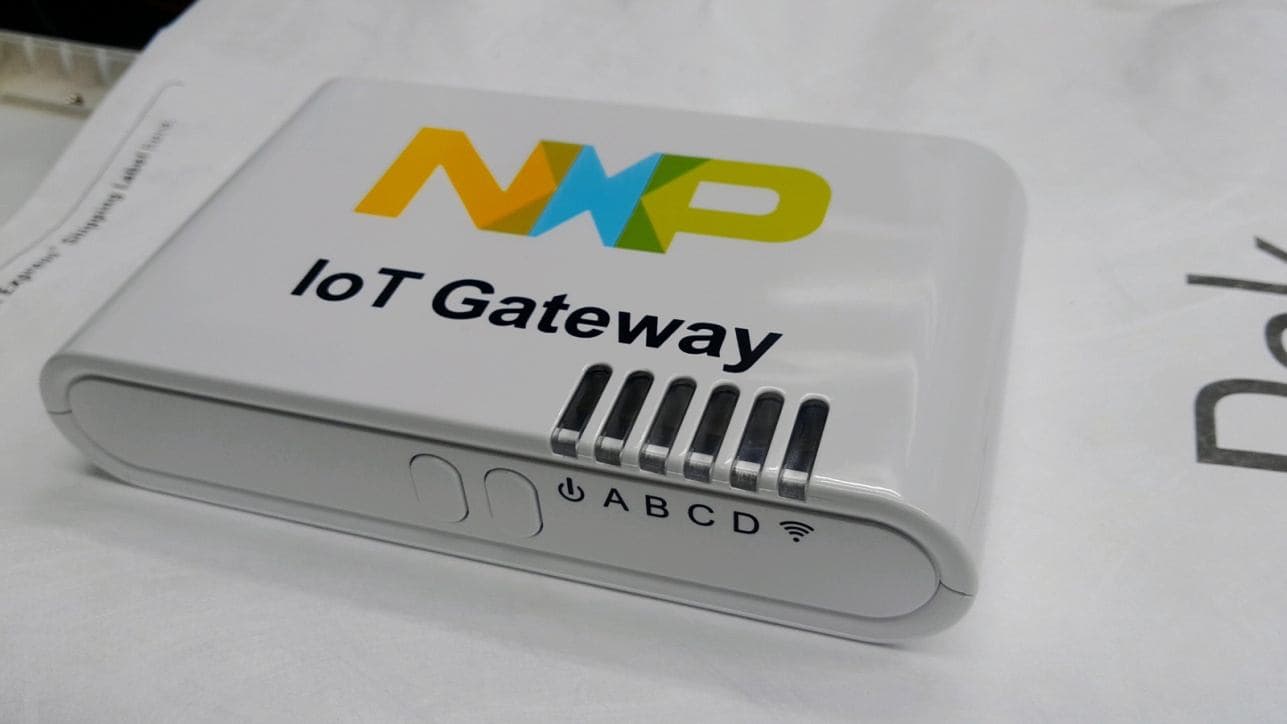
TYOJN5168IT00
Oct 22, 2013JN5168-RD6040-IoT Gateway
Equipment Class
DTS - Digital Transmission System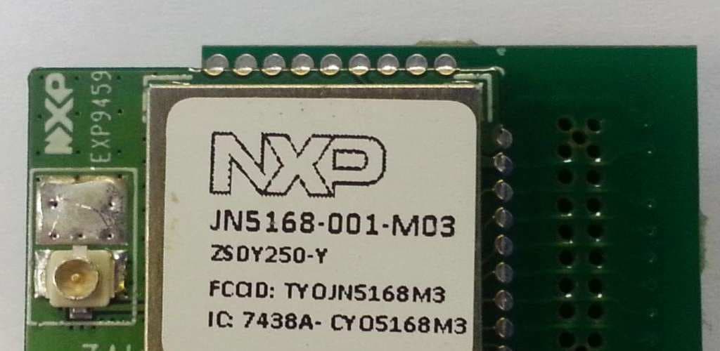
TYOJN5168M3
Jan 08, 2013JN5168-��1-M�3 IEEE802.15.4 Wireless Module
Equipment Class
DTS - Digital Transmission System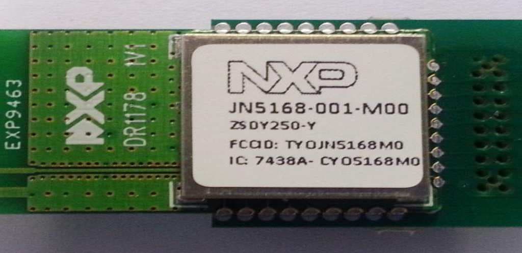
TYOJN5168M0
Jan 08, 2013JN5168-��1-M�� IEEE802.15.4 Wireless Module
Equipment Class
DTS - Digital Transmission System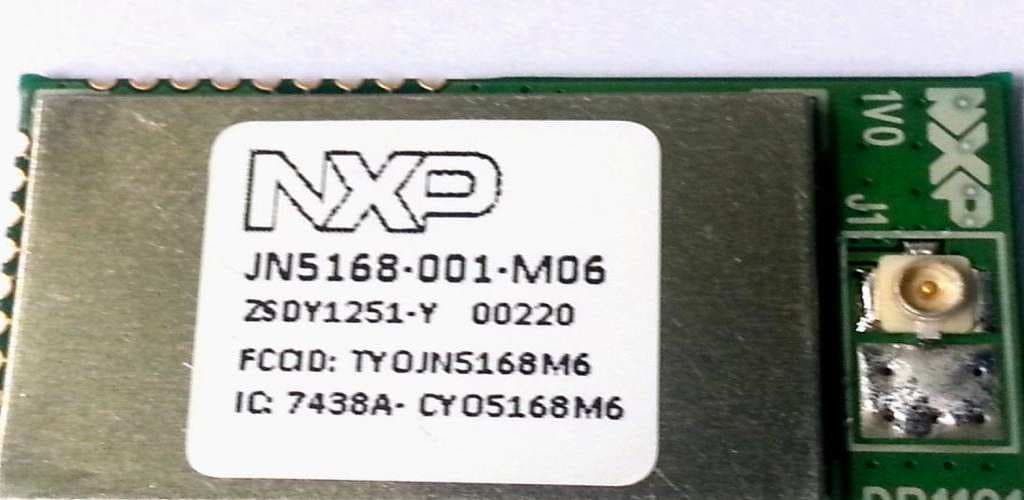
TYOJN5168M6
Jan 03, 2013JN5168-001-M�6 IEEE802.15.4 Wireless Module
Equipment Class
DTS - Digital Transmission System
TYOJN5168M5
Jan 03, 2013JN5168-001-M�5 IEEE802.15.4 Wireless Module
Equipment Class
DTS - Digital Transmission System