U7BWXTXT600PLUSUHF Transceiver
Shenzhen Wisetone Science & Technology Co., Ltd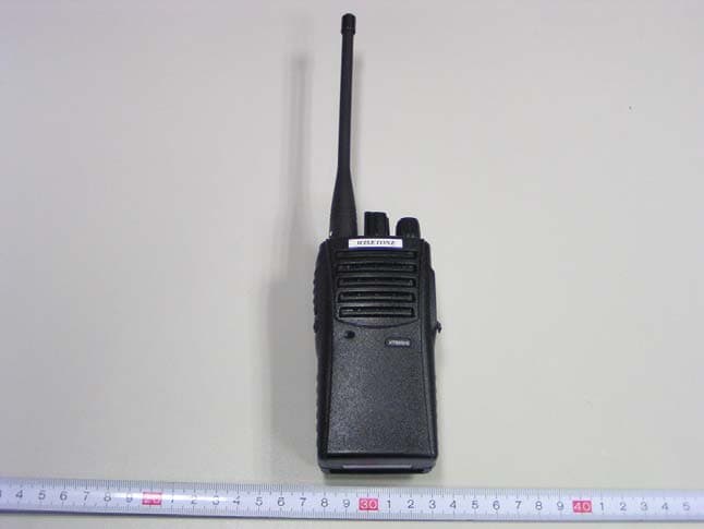
Click to zoom
Application Details
- Equipment Class
- TNF - Licensed Non-Broadcast Transmitter Held to Face
- Date of Grant
- Apr 19, 2007
- Application Purpose
- Original Equipment
- Date of Application
- Apr 19, 2007
- Equipment Note
- UHF Transceiver
- Frequency Range
- 430.00000000 - 470.00000000
- Country
- China
Documents & Files
Document Text
Text extracted from the exhibit documents filed with the FCC. Open a document above to read the original.
Users Manual
1 XT-600PLUS(4) Transceiver User manual 2 Wisetone science & technology Co., Ltd General This manual is intended for use by experienced technicians familiar with similar types of commercial grade communications equipment. It contains main required service information and data for the equipment. The following precautions are recommended for personal safety: 1、DO NOT transmit until all RF connectors are verified secure and any open connectors are properly terminated. 2、SHUT OFF and DO NOT operate this equipment near electrical blasting caps or in an explosive atmosphere. 3、This equipment should be maintained by qualified technicians only. 3 CONTENTS General Parts Description Specification of software Circuit Description CPU pins Description Parts list 1 Adjust Description and specifications Disassembly for Repair Component plans Parts list 2 Packing list FCB Component locations Principle View Principle diagram Transceiver model and specification MODEL FREQUENCY(MHz) POWERBATTERY CHARGER XT-600PLUS(4) 430~470MHz 4W XBP-1250 DC-791 fast charger 4 Parts Description 1、 Antenna The helical antenna is threaded plugs for the reception and transmission signal. 2、LED light Lights red while transmitting, green while receiving a signal. Flashes red when the battery voltage is low while transmitting. 3、Channel selector knob 4、Power switch/Volume control Turn the knob clockwise to switch the transceiver ON, anti-clockwise to turn off the power till there is a ”click” sound , rotate to adjust the volume level. 5、PTT switch(push to talk) Press the button while transmitting, and release it while receiving. 6、Monitor key Press it to shut off squelch, noise could be heard, release to connect squelch. 7、 Microphone Put in voice. 8、Speaker Put out voice. 9、Speaker jack Put down the cover, when you program you can put in the program line in it. 10、Battery 11、Charger plate Put the battery into the charger, it will operate when the charger plates touch the metal plates. 12、Battery deduction It use to close the battery, pull it up you can take out the battery. 5 Specification of the software function 1、 Turn the volume button can choice 15+1(scan) channels. 2、 Moni function. 3、 CTCSS/CDCSS program 4、 CTCSS: 50 groups 5、 CDCSS: 210 groups 6、 25KHz channel spacing 7、 Scan function, set scan channel. 8、 Power save. 9、 Time- out timer. 10、Voice number notice, program by Chinese/English. 11、VOX function and 9 levels can be choice. 12、9 levels squelch control. 13、Battery low-volt alarm. 14、Set ANI ID code number by program. 15、Remove the squelch tail function. 16、PC model. 17、Manual adjustment model. 18、Clone function Model description 1、 User mode Standard model (look for the XT-600PLUS(4) instruction manual) 2、PC mode Set and adjust the follow function numbers with PC software or programmer. (1) Channel RX and TX power. (2) Channel RX and TX tone. (3) BCL (busy channel lock) (4) TOT (TX time-out-timer) (5) Squelch level choice. (6) Power save function choice. (7) Voice alarm function choice. (8) Moni model choice. (9)Scan channel choice. (10)VOX level set. (11)Chinese/English number notice choice. (12)ANI ID number set. 3. manual adjustment mode High or low power by manual adjustment (1)make sure the channel and then close the transceiver. (2)press the PTT+MONI button to open the transceiver, it will be TX power adjustment model, the transceiver turn to the TX model. (3) loose the PTT+MONI button. (4)press the PTT button one time, the power will increase, press the MONI button one time, the power will reduce. (5) After you finish the adjustment please close the transceiver immediately, then if you open the transceiver again it will operate with the power which you have adjusted. 6 4 Clone function (1)Use the clone line connect clone radio with be-cloned radio. (2)Turn on the power of the be-cloned radio. (3)Chose the 16 channel. (4)Push the MONI button after turn off the power of clone radio, then turn on the power; it will come into clone model. (5) If the clone is successful the Green LED will light, or the Orange LED will light. Circuit Description 一、 Frequency configuration The receiver utilizes double conversion. The first IF is 38.85MHz and the second IF is 450KHZ. The first local oscillator signal is supplied from the PLL circuit. The PLL circuit in the transmitter generates the necessary frequencies. Fig.1 shows the frequencies. XT-600PLUS(4) Frequency range: 430 MHz—470MHz ANTSW RF AMP TX AMP TX DRIVER RX TX IF AMP CF 450KHz IF SYSTEM 38.4MHz AF AMP 12.8MHz PLL VCO MIC AMP Fig.1 Frequency configuration 二、 Receiver The receiver utilizes double conversion. 1. Front-end RF amplifier An incoming signal from the antenna is applied to an RF amplifier after passing through a transmit/receive switch circuit and a band pass filter. After the signal is amplified, the signal is filtered through a band pass filter to eliminate unwanted signals before it is passed to the first mixer. 7 ANT SW D211 BPF RF AMP T221 BPF MIXER T241 MCF FL251FL253 IF AMP T251 FL277 IF MIX U261 38.4MHz 1ST LOCAL OSC PLL AF AMP LPF HPF AF AMP SP U811 U411 Fig. 2 Receiver section configuration 2. First Mixer The signal from the RF amplifier is heterodyned with the first local oscillator signal from the PLL frequency synthesizer circuit at the first mixer (T241) to create a 38.85 MHz first intermediate frequency (1st IF) signal. The first IF signal is then fed through two monolithic crystal filters (FL251,FL253) to further remove spurious signals. 3. IF amplifier The first IF signal is amplified by T251, and then enters U261 (FM processing IC). The signal is heterodyned again with a second local oscillator signal within U261 to create a 450kHz second IF signal. The second IF signal is then fed through a 450kHz ceramic filter (FL277) to further eliminate unwanted signals before it is amplified and FM detected in U261. 4. AF amplifier The recovered AF signal obtained from U261, and de-emphasized by R264 and C264. The AF signal is then passed throug…
Text truncated - open the document above for the full version.
Block Diagram
LPFLPF TX Power AMP 2SC4226+2SK3078+2SK3476/RD07 Antenna SW HVC131x3 BPFBPF HF AMP 2SC4226 1st Mixer 2SC4226 TX/RX Switch KDS114x2 APC NJM2904V APC Sense BATTSB 5R 5R Buffer AMP 2SC4226 Modulator 2SC4226 RX VCO 2SC4226 TX VCO/ Controler TX/RX VCO KRC404x2 5C5C LPF Antenna DO Fin BPF 38.85MHz IF AMP KTC4080Y 5R 2nd LO 38.4MHz IF Mixer & Demodulator TA31136FN 5R RSSI SQL BPF 450KHz DET OSC 450KHz APC/TunePLL Circuit LMX 2332 Tripler KTC4080Y 5R t 5C DCS Input TCXO 12.8MHz LD Out PLL Data PLL EN PLL CLK MIC MUTE SW 5V MIC Mute 1 1/2 Vcc Ref. 1/4NJM324V 5V 5V5V 5V MIC Pre AMP 1/4NJM324V MIC AMP 1/4NJM324V VOX AMP 1/4NJM324V+KDS122 MIC MUTE SW MIC Mute 2 VOX Out TXD MIC JACK 3.5mm Modulation Addjuster N/W SW N/WN/W SW Speaker JACK 2.5mm PG AMP KRC404+KRA305 SB PG RXD AF AMP TDA7233 SB SP Mute Power SW KRA305x3 5V5C5R5T Save RX Control TX Control 2SK1824 KRC404 DC Regulator 5A BATTSB5V Volume Controler BEEP MPU S3P856B PLL Data PLL EN PLL CLK Save RX Control TX Control TXD RXD APC/Tune BATT Test VOX SQL CTCSS Input DCS CTCSS MIC Mute 1 MIC Mute 2 N/W SP Mute PG BEEP DCS/CTCSS Filter OSC 32.768KHz Reset Circuit 2SB624 5V PTT SW TC121V MONI SW TC121V Encoder EN0 EN1 EN2 EN3 EEPROM 24C08 DATA CLK PLL LD SW SW TX LED RX LED 5V SB KRA305 KRC404 BLOCK DIAGRAM LPFLPF 5T5T N/W SW 2SK1824 AGC KTC4075+KDS122 DC Regulator 5A 5M 5M KRC404 KRC404 N/W SW 2SK1824 DCS Balence Circuit PLL OSC Addjuster 5C TX Path RX Path 5R
External Photos
EXHIBIT B - EUT EXTERNAL PHOTOGRAPHS EUT – Front View EUT – Rear View
ID Label/Location Info
EXHIBIT A - FCC ID LABELING AND LOCATION Proposed FCC ID Labeling Proposed FCC ID Location ATTENTION! Restricted to occupational use to satisfy FCC RF exposure limits. See users manual for operating requirements. FCC ID: U7BWXTXT600PLUS Model: XT-600PLUS(4) ATTENTION! Restricted to occupational use to satisfy FCC RF exposure limits. See users manual for operating requirements. FCC ID: U7BWXTXT600PLUS Model: XT-600PLUS(4)
Internal Photos
EXHIBIT C - EUT INTERNAL PHOTOGRAPHS EUT – Uncovered View EUT – Inside View (1) EUT – Inside View (2) EUT – Inside View (3) EUT – Inside View (4) EUT – PCB Front View EUT – PCB Rear View
Operational Description
1 Circuit Description 一、 Frequency configuration The receiver utilizes double conversion. The first IF is 38.85MHz and the second IF is 450KHZ. The first local oscillator signal is supplied from the PLL circuit. The PLL circuit in the transmitter generates the necessary frequencies. Fig.1 shows the frequencies. XT-600 Frequency range:(1): 350 MHz—370MHz (2): 370 MHz—390MHz (3): 400 MHz—430MHz (4): 430 MHz—470MHz XT-500 Frequency range:(1): 136MHz---150MHz (2): 150MHz---174MHz ANTSWRF AMP TX AMPT X DRI VER RX TX IF AMP CF 450KHz I F SYSTEM 38. 4MHz AF AMP 12. 8MHz PL L VCO MIC AMP Fig.1 Frequency configuration 二、 Receiver The receiver utilizes double conversion. 1. Front-end RF amplifier An incoming signal from the antenna is applied to an RF amplifier after passing through a transmit/receive switch circuit and a band pass filter. After the signal is amplified, the signal is filtered through a band pass filter to eliminate unwanted signals before it is passed to the first mixer. ANT SW D211 BPF RF AMP T221 BPF MI X E R T241 MC F FL251 FL253 IF AMP T251 FL277 IF MIX U261 38. 4MHz 1 ST L OCAL OSC PLL AF AMP LPF HPF AF AMP SP U8 1 1 U4 1 1 2 Fig. 2 Receiver section configuration 2. First Mixer The signal from the RF amplifier is heterodyned with the first local oscillator signal from the PLL frequency synthesizer circuit at the first mixer (T241) to create a 38.85 MHz first intermediate frequency (1st IF) signal. The first IF signal is then fed through two monolithic crystal filters (FL251,FL253) to further remove spurious signals. 3. IF amplifier The first IF signal is amplified by T251, and then enters U261 (FM processing IC). The signal is heterodyned again with a second local oscillator signal within U261 to create a 450kHz second IF signal. The second IF signal is then fed through a 450kHz ceramic filter ( FL277) to further eliminate unwanted signals before it is amplified and FM detected in U261. 4. AF amplifier The recovered AF signal obtained from U261 , and de-emphasized by R264 and C264. The AF signal is then passed through U811 is amplified and low-pass filter and high-pass filter. The processed AF signal passes through an AF volume control and is amplified to a sufficient level to drive a loud speaker by an AF power amplifier (U411). 5. Squelch Part of the AF signal from the U261 is go into the U261 again, and the noise component is amplified and rectified by a filter and an amplifier to produce a DC voltage corresponding to the noise level. The DC signal from the U261 goes to the analog port of the microprocessor (U811). U811 determines whether to output sounds from the speaker, U811 sends a high signal to the MUTE and AFCO lines and turns U411 on through T490. (See Fig.3) U2 6 1 U8 1 1 U4 1 1 T498 T490 9 8 14 14 25 22 30 8 2 5 IF AMP DET HPF AMP DET HPF BUSY HPF AMP MU T E S W F AMP SW SP Fig.3. AF Amplifier and squelch 6. Receiving signaling CTCSS/CDCSS 300 Hz and audio frequencies of the output signal from IF IC are cut by a low-pass filter. The resulting signal enters the microprocessor ( U811). U811 determines whether the CTCSS or CDCSS matches the preset value, and controls the MUTE SW and the speaker output sounds according to the squelch results. 3 三、PLL frequency synthesizer The PLL circuit generates the first local oscillator signal for reception and the RF signal for transmission. 1. PLL The frequency step of the PLL circuit is 5 or 6.25KHz. A 12.8MHz reference oscillator signal is divided at U311 by a fixed counter to produce the 5 or 6.25KHz reference frequency. The voltage controlled oscillator (VCO) output signal is buffer amplified by T311, then divided in U311 by a dual-module programmable counter. The divided signal is compared in phase with the 5 or 6.25KHz reference signal in the phase comparator in U311. The output signal from the phase comparator is filtered through a low-pass filter and passed to the VCO to control the oscillator frequency. (See Fig. 4) CR311 12 .8 MHz PLL I C U3 1 1 PLL DATA I/N 5 KHz / 6 . 2 5 KHz PHASE COMPART OR CHARGE PUMP I/M 5KHz/6.25KHz LPF D322 D332 TX VCO RX VCO BUF F AMP T/ R SW T321 T331 T311 T304 T305 Fig. 4 PLL 2. VCO The operating frequency is generated by T321 in transmit mode and T331 in receive mode. The oscillator frequency is controlled by applying the VCO control voltage, obtained from the phase comparator, to the varactor diodes ( D322 in transmit mode and D332 in receive mode) . The T/R pin is set high in receive mode causing T304 and T305 to turn T321off, and turn T331 on. The T/R pin is set low in transmit mode. The outputs from T321 and T331 are amplified by T311, then sent to the PLL circuit U311 and receiver or transmitter. 四、Transmitter 3. Transmit audio The modulation signal from the microphone is amplified by U421, passes through a preemphasis circuit, and the signal then passes through a low-pass filter (splatter filter) ( T430 and T433) and cuts up 3kHz and higher frequencies. The resulting signal goes to the VCO for direct FM modulation. (See Fig. 5) 4. CTCSS/CDCSS encoder A necessary signal for CTCSS/CDCSS encoding is generated by U811 and 4 FM-modulated to the PLL reference signal. Since the reference OSC does not modulate the loop characteristic frequency or higher, modulation is performed at the VCO side by adjusting the balance. (See Fig. 5) MI C T417 SW U4 2 1 MI C A MP T430, T433 BPF VCO D321, D322 U8 1 1 CPU MU T E 31 44 71 20 DQT DT MF APC SW D141 T140 TX AMP T130 TX DRI VER T120 TX AMP APC U1 6 1 SW D111, D112 LPF 5T Fig. 5. Transmit audio CTCSS 5. RF amplifier The transmit signal obtained from the VCO buffer amplifier T311, is amplified by T140. This amplified signal is passed to the power amplifier T130 and T120, which consists of a 2 stage FET amplifier and is capable of producing up to 4W of RF power 6. ANT switch and LPF The RF amplifier output signal is passed through a low-pass filter network and a transmit/receive switching circuit before it is passed to the antenna terminal. The transmit…
Text truncated - open the document above for the full version.
Parts List/Tune Up Info
Adjust Description and specifications Use programmer or PC software to program XT-500/600 , or by manual program , eg . To program XT-500/600 by manual as follows: 一、Instrument:: Synthesized test instrument 1 set Scanner 1 set 3A/10V power 1 set Digital Voltmeter 1 set 3A DC Ammeter 1 set 二、Adjust: 1、Initialization: It is necessary to initialize the transceiver because there is useless data in EEPROM. So make initialization before adjust. After set the Initialization data on PC, connect the radio by program line, then turn on the radio power, you can write in Initialization data. 2、Adjustment: The adjustment of XT-500/600, some are conducted in PC communication mode, some are in manual program mode. Turn on the power and enter the manual program mode., VCO SECTION: measurement Adjustment ITEM CONDITION Te s t e q u i p terminalpart Method Specificati ons/Re mark 1、.Setting 1、power 7.5V 1、TX high frequency,enter the manual program mode and press the PTT 4.0V±0.1V 2、Transmit VCO1.CH: lock voltage 2、TX low frequency, enter the manual program mode and press the PTT CV321 >0.7V 1、RX high frequency,enter the manual program mode and press the MONI 3.8V±0.1V 3、Receive VCO1.CH: lock voltage 2、RX low frequency, enter the manual program mode and press the MONI Digital Vo l t m e t e r CV CV331 >0.7V Adjust the Transmitter section: Measurement Adjustment Item Condition Test equipTe r m i n a lparts Method Specificati ons /Remarks 7、Transmit frequency 1、TX center Turn to manual mode and press the PTT Synthetical test ANT RV361 Adjust to the center frequency the error≤ ±250Hz 8、MAX DEV 最大频偏 1、TX center frequency Turn to manual mode and press the PTT Synthetical test LPF: 15kHz AF:1kHz 120mV ANT MIC-Jack RV422 Adjust the frequency error to:4.2kHz±100Hz 9、FM Sensitivity 1、TX center Turn to manual mode and press the PTT Synthetical test FILTER: 0.3-3.4kHz AF:1kHz 15mV ANT MIC-Jack Check frequency error :2.2kHz-3.6kHz 1、TX center and with 67.0Hz CTCSS, turn to manual mode 67.0Hz CTCSS 10、 CTCSS balance 2、TX center and with 250.3Hz CTCSS, turn to manual mode and press the PTT Synthetical test LPF: 300Hz ANT Adjust VR3,the test value of on condition 1 & condition 2 is consistent, the difference value<=200Hz 250.3Hz CTCSS 11、CTCSS frequency error 1、TX center frequency CTCSS:67.0Hz turn to manual mode Adjust the frequency error to:0.65kHz±100Hz 12、CDCSS frequency error 1、TX center frequency CDCSS:023 turn to manual mode Synthetical test LPF:300Hz ANT Adjust the frequency error to:0.65kHz±100Hz 13、.Low Battery alarm level Turn to manual mode, Adjust the battery to 5.7V Digital voltmete Adjust so that the LED flashes Adjust the receiver section: (enter manual mode first) Measurement Adjustment Item Condition Te s t e q u i pTe r m i n a l parts Method Specificati ons /Remarks 4、.Band-pass filter 1、RX center turn to channel 4 in manual mode Spectrum analyz ANT . Adjust the undee to the top, the bandwidth is about 20MHz, the sign of central frequency is in the middle of the undee 1、RX center Turn to manual mode 2、RX low Turn to manual mode 5、Sensitivity 3、RX high Turn to manual mode Synthetical test SSG output: -118dBm MOD:1KHz DEV:±3kHz FILTER: 0.3-3.4kHz ANT MIC-Jack check SINAD: 12dB or higher 1、RX center Turn to manual mode Synthetical test SSG output: -117dBm Level 9 Adjust to close the squelch. Adjust the Level 9 squelch. 6、Squelch 2、RX center Turn to manual mode Synthetical test SSG output: -125dBm ANT MIC-Jack RV266 Level 3 Adjust to close the squelch. Adjust the Level 3 squelch.
Schematics
E422 4.7uF C836 104P C410 473P R135 0R C111 22P C118 102P R110 47K I C122 470P C135 39P C134 3P C113 470P C136 N/F C133 47P C141 103P C104 N/F C108 N/F C103 104P C132 102P C142 470P C131 1P C144 33P C143 7P R113 220R R104 N/F R105 N/F R132 47R R106 N/F R144 N/F R142 22R R103 0R R131 47R D112 HVC131 L111 4T L112 4T L113 220nH L237 27nH L141 33nH L134 6.8nH L121 7T L131 33nH T120 2SK3476 T140 2SC4226 T104 N/F ANT111 3411-00000-DA C146 9P C148 103P R147 10K R146 2.7K R148 10K R249 10K R314 180R R312 180R R313 33R R321 180R L247 22nH L321 220nH D141 KDS114 D249 KDS114 C247 3P C248 N/F C312 8P C316 N/F C315 6P C249 3P T311 2SC4226 T321 2SC4226 C321 15P C322 6P C323 6P C325 0.5P C328 15P C326 0.5P C324 9P D322 KDV154 D321 KDV154 R325 100K L323 220nH L322 4T CV321 6PF R335 10K R331 180R L331 220nH T331 2SC4226 C331 15P C332 6P C333 6P L332 4T CV331 6PF R305 47R R304 100R R315 10K R316 2.7K C311 2P D332 KDV154 C334 12P C309 104P C305 4.7uF C335 470P L333 220nH R306 10K R307 10K C307 470P C308 N/F C306 470P R311 100R C304 470P L211 5T L215 7T L221 100nH L216 7T L227 7T R216 100K R215 100K R221 100R R218 56K R254 150K R253 680R C215 13P C212 24P C213 27P C217 N/F C218 18P C216 13P C235 33P C228 7P C236 6P C224 13P C226 3P C222 N/F C227 13P C237 33P C251 33P C253 10P C252 1.5P D215 KDV154 D216 KDV154 T221 2SC4226 D227 KDV154 T241 2SC4226 FL251 38.85MHZ FL253 38.85MHZ R255 3.3K C255 103P C256 103P R256 220R L224 7T C223 9P C225 9P D224 KDV154 R227 100K R224 100K C233 103P C246 103P R245 68R R246 220R R242 4.7K R243 4.7K R241 15K C243 6P T130 2SK3078 T202 KRA305 T101 KRA305 T301 KRA305 T305 KRC404 T304 KRC404 T251 KTC4080Y O S C i n 1 D e c 6 F I L o u t 7 I F o u t 1 1 I F i n 5 M I X i n 1 6 A F o u t 9 R S S I 1 2 Q U A D 1 0 M I X o u t 3 O S C o u t 2 F I L i n 8 N - d e t 1 3 N - r e c 1 4 V c c 4 G N D 1 5 U261 TA31136F C293 102P C282 104P C261 224P C 2 9 1 33P C278 104P C 2 8 1 1 0 4 P C292 56P C262 82P C263 224P C268 330P C271 330P L291 1uH R291 22K R271 220K R263 3.3K CR291 38.4MHZ CR262 JTB455CM T263 KRC404 R264 22k R266 N/F R265 N/F C265 222P C266 222P RV266 50K C264 472P R267 0R R268 270K R272 3.3K R273 680R T273 KRC404 C277 103P IO FL277 M55FW E261 22uF/10V R332 10K R333 10K R322 10K T103 N/F R107 N/F C123 4.7uFR143 8.2K R133 2.7K L135 220nH R136 100R C214 4P C221 103P C232 103P C231 103P C234 103P L243 820nH C245 22P R244 100R C241 103P C254 103P R262 3.9K G N D 1 M u t e 2 + V S 4 O u t p u t 5 S V R 6 G N D 3 - I n p u t 7 + I n p u t 8 U411 TDA7233 E481 22uF/10V R478 1K E473 100uF/6V3 R475 4.7M R476 N/F T481 KRA305 R481 10K R482 1K R483 N/F C483 N/F 2 5 4 1 JK471 ST301 2 5 4 1 JK451 ST104 SP471 SPEAKER MIC451 MIC R451 N/F C451 470P C452 472P R452 15K L454 4.7uH 2 3 1 4 1 1 U421A NJM324 6 5 7 U421B NJM324 9 10 8 U421C NJM324 13 12 14 U421D NJM324 R456 0R R413 470K R411 1K8 R412 2K7 R414 2K2 R417 1K R421 560K C412 472P C411 563P C413 273P C414 273P C415 4.7uF R445 330K C447 470P C440 104P R440 10R C441 104P C445 104P R442 20K R441 33K R444 100K C446 1uF SB BATT B A T T S B 5T SB VAF PG 5V 5T5T5T 5 T 5 T SBTX 5R 5R5R TUNETUNE 5C L311 27nH T/R TUNE VR411A RD810SRD810S/10K D211 HVC131 C211 22P BATT SB VAF AFI A F M U T E S P PG SW833 SW834 PTT MONI PTT MONI RXD BATT BATTERY 1/2 Vcc N / W N/W N/W 5T 5C 5V5V5V 5V R257 100R V-RX V - R X V-RX 5R PR802 1K C302 N/F C101 103P C201 103P C301 103P C102 103P C202 103P P T T M O N I R X D P G M U T E S P A P C / T U N E M I C O A F S B PTT MONI RXD PG MIC MUTE2 MUTE SP APC/TUNE MICO AF SB PTT MONI RXD PG MIC MUTE2 MUTE SP APC/TUNE MICO AF SB PTT MONI RXD PG MIC MUTE2 MUTE SP APC/TUNE AF SB N/W PTT MONI RXD PG MIC MUTE2 MUTE SP APC/TUNE AF SB VOICE SDA N/W PR804 47K PR801 47K A 0 1 A 1 2 G N D 4 D A 5 C K 6 A 2 3 W P 7 V c c 8 U835 24CXX C835 N/F R808 47K R807 NU 5V5V 5R 5T 5C5C 5T RXC TXC VCOC RXC TXC VCOC AB 1 2 3 4 5 CDEFGHIJKLM 1 2 3 4 5 ABCDEFGHIJKLM SCHEMATIC DIAGRAM SQ SQ PLL PS PLL LE PLL DATA PLL CLK EN1 EN2 EN3 EN4EN4 EN3 EN2 EN1 L142 6.8nH R108 N/F R835 0R R836 N/F R806 47K D821 HT15-22SVGC/TR8 SDA C492 47P C494 104P C491 104P C493 104P R492 4M7 R494 22K R493 100K R491 470K E491 1uF/16V D491 KDS122 1/2 Vcc R323 100K D111 HVC131 2011-14055-22 2011-16073-232011-16073-23 2011-16073-23 2011-16073-23 2011-14046-232011-14046-23 2011-14046-23 2011-14046-23 2011-16073-23 C837 104P C834 N/F C117 5P C114 N/F C116 2P C128 6P C126 18P C127 N/F C112 10P C125 30P C124 4.7uF C257 4.7uF C276 4.7uF C115 9P R121 0.1R C121 4.7uF C474 4.7uF C475 4.7uF C473 0.1uF R473 2.2R C472 220P C471 220P C454 220P C838 220P C458 221P R410 0R C457 104P (1601-54002-00) R101 0R L372 220nH L371 10uH R362 1K V c c 1 1 V p 1 2 D o R F 3 G N D _ D 4 f i n R F 5 f i n R F 6 G N D _ A 7 O S C i n 8 G N D _ D 9 F o L D 1 0 C l o c k 1 1 D a t a 1 2 L E 1 3 G N D _ A 1 4 f i n I F 1 5 f i n I F 1 6 G N D _ D 1 7 D o I F 1 8 V p 2 1 9 V c c 2 2 0 U311 LMX2332 C362 101P C371 102P R373 1K C372 102P R378 39K C377 102P R379 33K C376 104P R380 180R C361 102P R361 47R C370 102P R365 560R C368 101P R364 560R C367 101P R368 2K2 C366 101PR363 6K8 R367 4K7 E363 0.1uF E362 1uF E361 0.1uF D361 1N4148 XOUT 3 VC 1 5C 4 GND 2 CR311 12.8MHz RV361 50K E365 10uF L376 101T R376 0R R360 150R E371 4.7uF R383 22K R385 22K C382 104P 5C C364 470P E373 4.7uF C365 NC R369 150K R370 NC 5V T361 2SC4226 L361 18nH C360 470P C363 2P L362 100nH C381 47P R375 220R T362 KTC4080Y C386 82P R374 10K L364 100nH L363 180nH C385 102P R381 100R 5R C384 390P C387 120P R366 1K C375 104P C373 10P C378 10P C379 33P C383 68P R425 1K8 R427 33K C426 473P R426 4K7 C436 470P R439 100R R438 3K3 R437 1K8 T571 2SK1824 R384 4K7 R371 4K7 R372 47K R567 220K C389 223P C388 103P R566 68K R561 220KR565 33K R382 2K7 C555 104P R556 10K R551 120K R555 22K C554 470P R554 100R R553 3K3 R552 1K8 T551 2SK1824 C661 470P R564 100R R563 3K3 R562 1K8 T561 2SK1824 C583 470P R584 100R R582 3K3 R581 1K8 T581 2SK1824 C151 102P E151 4.7uF R167 150K R164 150K R165 150K R166 150K R163 150K R161 150K R153 10K R162 NC R155 220K R154 47K R156 NC R152 1M R151 10…
Text truncated - open the document above for the full version.
Test Report
Note: This test report is for the customer shown above and their specific product only. It may not be duplicated or used in part without prior written consent from Bay Area Compliance Laboratory Corp. (Shenzhen). This report must not be used by the customer to claim product certification, approval, or endorsement by NVLAP, NIST or any agency of the Federal Government. FCC PART 90 TYPE APPROVAL EMI MEASUREMENT AND TEST REPORT For Shenzhen Wisetone Science & Technology Co., Ltd New Industrial Zone, Dabutou, Songyuan, Guanlan, Bao’an District, Shenzhen, China FCC ID: U7BWXTXT600PLUS This Report Concerns: Original Report Equipment Type: UHF Transceiver Test Engineer: William Chan Report No.: RSZ07031301 Test Date: 2007-03-16 to 2007-03-31 Report Date: 2007-04-02 Reviewed By: EMC Manager: Boni Baniqued Prepared By: Bay Area Compliance Laboratory Corp. (Shenzhen) 6/F, the 3rd Phase of WanLi Industrial Building, ShiHua Road, FuTian Free Trade Zone Shenzhen, Guangdong, China Tel: +86-755-33320018 Fax: +86-755-33320008 Shenzhen Wisetone Science & Technology Co., Ltd FCC ID: U7BWXTXT600PLUS Report #: RSZ07031301 Page 2 of 28 FCC PART 90 Report TABLE OF CONTENTS GENERAL INFORMATION.......................................................................................................................................4 PRODUCT DESCRIPTION FOR EQUIPMENT UNDER THE TEST (EUT) ..............................................................................4 OBJECTIVE...................................................................................................................................................................4 RELATED SUBMITTAL(S)/GRANT(S).............................................................................................................................4 TEST METHODOLOGY..................................................................................................................................................4 TEST FACILITY.............................................................................................................................................................4 SYSTEM TEST CONFIGURATION ..........................................................................................................................6 DESCRIPTION OF TEST CONFIGURATION......................................................................................................................6 EQUIPMENT MODIFICATIONS.......................................................................................................................................6 CONFIGURATION OF TEST SETUP.................................................................................................................................7 BLOCK DIAGRAM OF TEST SETUP................................................................................................................................7 SUMMARY OF TEST RESULTS ...............................................................................................................................8 §1.1310 §2.1093 - RF EXPOSURE ...............................................................................................................................9 §2.1046 - CONDUCTED OUTPUT POWER............................................................................................................10 APPLICABLE STANDARD............................................................................................................................................10 TEST EQUIPMENT LIST AND DETAILS.........................................................................................................................10 TEST PROCEDURE......................................................................................................................................................10 TEST DATA................................................................................................................................................................10 §2.1046 and §90.205 – RADIATED OUTPUT POWER ..........................................................................................12 APPLICABLE STANDARD............................................................................................................................................12 TEST EQUIPMENT LIST AND DETAILS.........................................................................................................................12 TEST PROCEDURE......................................................................................................................................................12 TEST DATA................................................................................................................................................................13 §2.1047 and §90.207 - MODULATION CHARACTERISTIC ................................................................................14 APPLICABLE STANDARD............................................................................................................................................14 TEST EQUIPMENT LIST AND DETAILS.........................................................................................................................14 TEST PROCEDURE......................................................................................................................................................14 TEST DATA................................................................................................................................................................14 §2.1049 and § 90.209 – OCCUPIED BANDWIDTH ................................................................................................17 APPLICABLE STANDARD............................................................................................................................................17 TEST EQUIPMENT LIST AND DETAILS......................................................................…
Text truncated - open the document above for the full version.
Contact Information
Applicant
Yuangui Xiao
Test Firm
Bay Area Compliance Laboratory Corp. (Shenzhen)John Chan
Technical Specifications
| # | Rule Parts | Frequency Range | Power Output | Emission | Tolerance |
|---|---|---|---|---|---|
| 1 | 90 | 430 MHz - 470 MHz | 3.8 W | 16K0F3E | 5.0000000000 ppm |