UCAMF101RARemote Control for Toba Magic Fountain (434MHz Tx)
Toba Fountains L.L.C.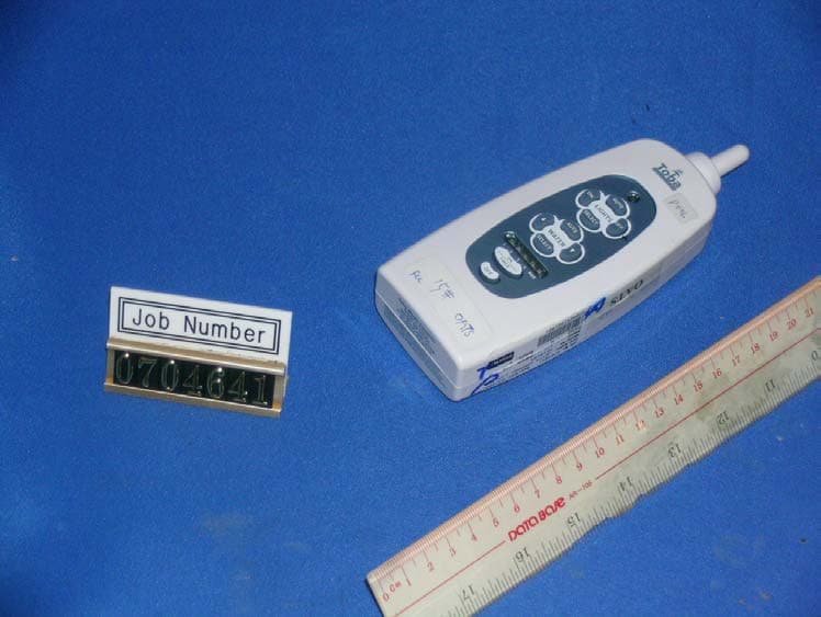
Click to zoom
Application Details
- Equipment Class
- DSC - Part 15 Security/Remote Control Transmitter
- Date of Grant
- Apr 01, 2007
- Application Purpose
- Original Equipment
- Date of Application
- Apr 01, 2007
- Equipment Note
- Remote Control for Toba Magic Fountain (434MHz Tx)
- Frequency Range
- 434.00000000 - 434.00000000
- Company
- Toba Fountains L.L.C.
- Country
- United States
Documents & Files
Document Text
Text extracted from the exhibit documents filed with the FCC. Open a document above to read the original.
Block Diagram
MICRF102 Micrel MICRF102 6 December 2006 Functional Description The block diagram illustrates the basic structure of the MICRF102. Identifi ed in the fi gure are the principal functional blocks of the IC, namely the (1, 2, 3, 4, 5) UHF Synthesizer, (6a/b) Buffer, (7) Antenna tuner, (8) Power amplifi er, (9) TX bias control, (10) Reference bias and, (11) Process tuner. The UHF synthesizer generates the carrier frequency with quadrature outputs. The in-phase signal (I) is used to drive the PA and the quadrature signal (Q) is used to compare the antenna signal phase for antenna tuning purposes. The Antenna tuner block senses the phase of the transmit signal at the antenna port and controls the varactor capacitor to tune the antenna. The Power control unit senses the antenna signal and con- trols the PA bias current to regulate the antenna signal to the transmit power. Block Diagram TX Bias Control Varactor Device Antenna Tuning Control Power Amp Buffer VSS ANTM ANTP ASK Buffer Prescaler Divide by 32 REF.OSC PC VDD VDD (10) (5) (2) Reference Oscillator (1) VCO (4) (3) (9) (8) (7) (11) (6a) (6b) STBY Reference Bias Phase Detector The Process tune circuit generates process independent bias currents for different blocks. A PCB antenna loop coupled with a resonator and a resistor divider network are all the components required to construct a complete UHF transmitter for remote actuation applications such as automotive keyless entry. Included within the IC is a differential varactor that serves as the tuning element to insure that the transmit frequency and antenna are aligned with the receiver over all supply and temperature variations.
External Photos
External Photo FCC ID : UCAMF101RA External Photo - front External Photo - rear
ID Label/Location Info
Label Location & Label Size: 45x24mm
Internal Photos
Internal Photo FCC ID : UCAMF101RA Internal Photo - 1 Internal Photo - 2 Internal Photo FCC ID : UCAMF101RA Internal Photo - 3
Operational Description
December 2006 1 MICRF102 MICRF102 Micrel MICRF102 QwikRadio™ UHF ASK Transmitter General Description The MICRF102 is a single chip Transmitter IC for remote wireless applications. The device employs Micrel’s latest Qwi- kRadio™ technology. This device is a true “data-in, antenna- out” monolithic device. All antenna tuning is accomplished automatically within the IC which eliminates manual tuning, and reduces production costs. The result is a highly reliable yet extremely low cost solution for high volume wireless applications. Because the MICRF102 is a true single-chip radio transmitter, it is easy to apply, minimizing design and production costs, and improving time to market. The MICRF102 uses a novel architecture where the external loop antenna is tuned to the internal output stage. This trans- mitter is designed to comply with worldwide UHF unlicensed band intentional radiator regulations. The IC is compatible with virtually all ASK/OOK (Amplitude Shift Keying/On-Off Keyed) UHF receiver types from wide-band super-regenerative radios to narrow-band, high performance super-heterodyne receiv- ers. The transmitter is designed to work with transmitter data rates from 100 to 20k bits per second. The automatic tuning, in conjunction with the external resistor, ensures that the transmitter output power stays constant for the life of the battery. When used with Micrel’s family of QwikRadio™ receivers, the MICRF102 provides the lowest cost and most reliable remote actuator and RF link system available. Data sheets and support documentation can be found on Micrel’s web site at: www.micrel.com. Typical Application PC VDD VSS REFOSC ASK MICRF102 ASK DATA INPUT RP2 6.8k 0.1μF 4.7μF RP1 100k +5V +5V Y1 ANTP ANTN STBY 100k C3 12pF 50V (2.7pF 50V) C2 8.2pF 50V (4.7pF 50V) PCB Antenna L1 Features • Complete UHF transmitter on a monolithic chip • Frequency range 300MHz to 470MHz • Data rates to 20kbps • Automatic antenna alignment, no manual adjustment • Low external part count • Low standby current <0.04μA Applications • Remote Keyless Entry systems (RKE) • Remote fan/light control • Garage door opener transmitters • Remote sensor data links • Tire Pressure Monitoring System (TPMS) • Telemetry Micrel, Inc. • 2180 Fortune Drive • San Jose, CA 95131 • USA • tel + 1 (408) 944-0800 • fax + 1 (408) 474-1000 • http://www.micrel.com QwikRadio is a trademark of Micrel, Inc. The QwikRadio ICs were developed under a partnership agreement with AIT of Orlando, Florida QwikRadio™ Ordering Information Part NumberTemperature Range Package StandardPb-Free MICRF102BMMICRF102YM-40°C to +85°C8-Pin SOIC MICRF102 Micrel MICRF102 2 December 2006 Pin Description Pin Number Pin Name Pin Function 1 PC Power Control Input. The voltage at this pin should be set between 0.15V to 0.35V for normal operation. 2 VDD Positive power supply input for the IC. This pin requires a large capacitor for ripple decoupling. A 4.7μF is recommended. 3 VSS This pin is the ground return for the IC. A power supply bypass capacitor connected from V DD to V SS should have the shortest possible path. 4 REFOSC This is the timing reference frequency which is the transmit frequency di- vided by 32. Connect a crystal (mode dependent) between this pin and V SS , or drive the input with an AC-coupled 0.5V PP input clock. See “Reference Oscillator” section in this data sheet. The crystal needs to have a 10pF load capacitance. 5 STBY Input for transmitter stand by control pin is pulled to V DD for transmit opera- tion and V SS for stand-by mode. The device requires 0.0 volts to be placed in stand by. 6 ANTN Negative RF power output to drive the low side of the transmit loop antenna. The RF output stage is tuned in the data transitions in the ASK pin. 7 ANTP Positive RF power output to drive the high side of the transmit loop antenna. The RF output stage is tuned in the data transitions in the ASK pin. 8 ASK Amplitude Shift Key modulation data input pin. For CW operation, connect this pin to V DD . Several transitions of highs and lows are required to tune the output RF stages. Pin Confi guration 1PC VDD VSS REFOSC 8 ASK ANTP ANTN STBY 7 6 5 2 3 4 8-Pin SOIC (M) December 2006 3 MICRF102 MICRF102 Micrel Electrical Characteristics (Note 4) Specifi cations apply for 4.75V < V DD < 5.5V, V PC = 0.35V, T A = 25°C, freq REFOSC = 12.1875MHz, STBY = V DD . Bold values indicate -40°C ≤ T A ≤ 85°C unless otherwise noted. Parameter Condition Min Typ Max Units Power Supply Standby Supply Current, I Q V STBY < 0.5V, V ASK < 0.5V or V ASK > V DD – 0.5V 0.04 μA MARK Supply Current, I ON @315MHz, Note 5 6 10.5 mA @433MHz, Note 5 8 12 mA SPACE Supply Current, I OFF @315MHz 4 6 mA @433MHz 6 8.5 mA Mean Operating Current 33% mark/space ratio at 315MHz, Note 5 4.7 mA 33% mark/space ratio at 433MHz, Note 5 6.7 mA RF Output Section and Modulation Limits: Output Power Level, P OUT @315MHz; Note 5, Note 6 –4 dBm @433MHz; Note 5, Note 6 –4 dBm Harmonics Output, Note 7 @315MHz 2nd harm. –46 dBc 3rd harm. –45 @433 MHz 2nd harm. –50 dBc 3rd harm. –41 Extinction Ratio for ASK 40 52 dBc Varactor Tuning Range Note 8 3 5 7 pF Reference Oscillator Section Reference Oscillator Input 300 kΩ Impedance Reference Oscillator Source 6 μA Current Reference Oscillator Input 0.2 0.5 V PP Voltage (peak-to-peak) Note 1. Exceeding the absolute maximum rating may damage the device. Note 2. The device is not guaranteed to function outside its operating rating. Note 3. Devices are ESD sensitive. Handling precautions recommended. Human body model, 1.5k in series with 100pF. Note 4. Specifi cation for packaged product only. Note 5. Supply current and output power are a function of the voltage input on the PC (power control) pin. All specifi cations in the “Electrical Charac- teristics” table applies for condition V PC = 350mV. Increasing the voltage on the PC pin will increase transmit power and also increase MARK supply current. Refer to the graphs “Output Power Versus PC Pin Voltage” and “Mark Current Versus …
Text truncated - open the document above for the full version.
Schematics
123456 A B C D 654321 D C B A 1 Jetta Co.Ltd 1 Fountain Remoter 00101 04 19-Jan-200709:25:59 H:\zxh\00101\Bei tian xin\Remoter\00101-003-0040(04-02).ddb - Documents\Telecontrol (04-02A).Sch Title Size:Number: Date: File: Revision: Sheetof Time: B Checked By: Approved By: Drawed By: (RESET) PC6 29 PD0 (RXD) 30 PD1 (TXD) 31 PD2(INT0) 32 PD3 (INT1) 1 PD4 (XCK/T0) 2 V C C 6 G N D 3 PB6 (XTAL1/TOSC1) 7 PB7 (XTAL2/TOSC2) 8 PD5 (T1) 9 PD6 (AIN0) 10 PD7 (AIN1) 11 PB0 (ICP) 12 PB1 (OC1A) 13 PB2 (SS/OC1B) 14 PB3 (MOSI/OC2) 15 PB4 (MISO) 16 PB5 (SCK) 17 AVCC 18 AREF 20 GND 21 (ADC0) PC0 23 (ADC1) PC1 24 (ADC2) PC2 25 (ADC3) PC3 26 (ADC4/SDA) PC4 27 (ADC5/SCL) PC5 28 ADC6 19 ADC7 22 V C C 4 G N D 5 U3 ATMEGA48_TQFP32 L5 1uH C7 104 S4 SW-PB S7 SW-PB S10 SW-PB S1 SW-PB S2 SW-PB S5 SW-PB S8 SW-PB S6 SW-PB S9 SW-PB S3 SW-PB D3 4H D4 3H D5 2H D6 1H D2 HMax R3 1K R4 1K R5 1K R6 1K R7 1K MISO SCK MOSI 12 34 56 78 910 JP1 Debug MOSI MISO SCKGND VDD RESETRESET PC 1 VDD 2 VSS 3 REFOSC 4 STBY 5 ANTM 6 ANTP 7 ASK 8 U1 MICRF102BM R10 100K R13 3.9K C16 100pF Y1 13.56MHz C4 104 +5V C19 1pF C17 100pF C18 100pF L4 56NH L3 56NH C21 2.2pF C20 2.2pF R14 1pF P1 RCA R11 100K Q1 S8050D BT1 4.5V DataSend DataSend DataSend AVCCHMax 4H 3H 2H 1H HMax 1H 2H 3H 4H Column0 Column1 Column2 Column3 Row0 Row1 Row2 Row0 Row1 Row2 Column0 Column1 Column2 Column3 R25 100k 1% R23 430k 1% VBT 1H 2H 3H 4H HMax RESET D7 TxLED R8 1K RF Transmintor Key Array Debug Interface Status Led MCU AVCC C8 104 LowVoltageDetect VDD PWMControl GND L1 180uH D1 MA2Q735 VBT R24 430k 1% R26 1 0 0 K 1 % +5V C2 104 PWMControl RF_SendEn PWMControl R12 10k VDD Q2 S8550D GND R2 1K RF_SendEn RF_SendEn R1 1K R9 10K +5V VDD C3 104 C6 104 Q3 S8050D R21 4.7k R20 20K PowerManage 1 2 3 4 5 6 7 8 9 J1 CON9 +5V SH/LD 1 CLK 2 E 3 F 4 G 5 H 6 QH 7 G N D 8 QH 9 SER 10 A 11 B 12 C 13 D 14 CLK INH 15 V C C 1 6 U2 74HC165 GND GND SCK MISO +5V C5 104 KeyEn Coder Setting R19 20K KeyEn RF_SendIndicate RF_SendIndicate RF_SendIdicate C22 22pF C23 22pF Y2 8MHz TXD RXD RXDTXD C13 100uF C15 10uF C14 100uF R27 0 R28 0 C24 104 R29 10K C26 104 R17100K R18 100K R30 100K R31 100K R32 100K R33 100K R34 100K R35 100K T1 T2 T3 T4 T5 T6 T7 F1 FUSE 250MA PTC T8 T9 L2 18NH xhzhangxhzhang mqu zymo
Test Report
• The test results reported in this test report shall refer only to the sample actually tested and shall not refer or be deemed to refer to bulk from which such a sample may be said to have been obtained. • This report shall not be reproduced except in full without prior authorization from Intertek Testing Services Hong Kong Limited. • For Terms And Conditions of the services, it can be provided upon request. • The evaluation data of the report will be kept for 3 years from the date of issuance. Intertek Testing Services Hong Kong Ltd. 2/F., Garment Centre, 576 Castle Peak Road, Kowloon, Hong Kong. Tel: (852) 2173 8888 Fax: (852) 2785 5487 Website: www.hk.intertek-etlsemko.com Toba Fountains L.L.C. Application For Certification (FCC ID: UCAMF101RA) Transmitter 0704641 BC/ Sandy Lee March 30, 2007 INTERTEK TESTING SERVICES FCC ID: UCAMF101RA i LIST OF EXHIBITS INTRODUCTION EXHIBIT 1: General Description EXHIBIT 2: System Test Configuration EXHIBIT 3: Emission Results EXHIBIT 4: Equipment Photographs EXHIBIT 5: Product Labelling EXHIBIT 6: Technical Specifications EXHIBIT 7: Instruction Manual EXHIBIT 8: Miscellaneous Information INTERTEK TESTING SERVICES FCC ID: UCAMF101RA ii MEASUREMENT/TECHNICAL REPORT Toba Fountains L.L.C. - MODEL: MF101RA FCC ID: UCAMF101RA March 30, 2007 This report concerns (check one:) Original Grant X Class II Change Equipment Type: Low Power Transmitter (example: computer, printer, modem, etc.) Deferred grant requested per 47 CFR 0.457(d)(1)(ii)? Yes No X If yes, defer until: date Company Name agrees to notify the Commission by: date of the intended date of announcement of the product so that the grant can be issued on that date. Transition Rules Request per 15.37? Yes No X If no, assumed Part 15, Subpart C for intentional radiator - the new 47 CFR [04-05-05 Edition] provision. Report prepared by: Ho Wai Kin, Ben Intertek Testing Services Hong Kong Ltd. 2/F., Garment Center, 576, Castle Peak Road, Kowloon, Hong Kong. Phone: 852-2173-8505 Fax: 852-2371-0521 INTERTEK TESTING SERVICES FCC ID: UCAMF101RA iii Table of Contents 1.0 General Description..............................................................................................2 1.1 Product Description ..............................................................................................2 1.2 Related Submittal(s) Grants .................................................................................2 1.3 Test Methodology.................................................................................................3 1.4 Test Facility ..........................................................................................................3 2.0 System Test Configuration ...................................................................................5 2.1 Justification ..........................................................................................................5 2.2 EUT Exercising Software .....................................................................................5 2.3 Special Accessories .............................................................................................5 2.4 Equipment Modification ........................................................................................6 2.5 Measurement Uncertainty ....................................................................................6 2.6 Support Equipment List and Description ..............................................................6 3.0 Emission Results ..................................................................................................8 3.1 Field Strength Calculation ....................................................................................9 3.2 Radiated Emission Configuration Photograph ....................................................10 3.3 Radiated Emission Data.....................................................................................11 4.0 Equipment Photographs .....................................................................................14 5.0 Product Labelling ................................................................................................16 6.0 Technical Specifications ....................................................................................18 7.0 Instruction Manual ..............................................................................................20 8.0 Miscellaneous Information .................................................................................22 8.1 Measured Bandwidth .........................................................................................23 8.2 Discussion of Pulse Desensitization ...................................................................24 8.3 Calculation of Average Factor ............................................................................25 8.4 Emissions Test Procedures................................................................................26 INTERTEK TESTING SERVICES FCC ID: UCAMF101RA iv List of attached file Exhibit type File Description filename Test Report Test Report report.pdf Operation Description Technical Description descri.pdf Test Setup Photo Radiated Emission radiated photos.doc Test Report Bandwidth Plot bw.pdf External Photo External Photo external photos.doc Internal Photo Internal Photo internal photos.doc Block Diagram Block Diagram block.pdf Schematics Circuit Diagram circuit.pdf ID Label/Location Label Artwork and Location label.pdf User Manual User Manual manual.pdf Test Report Timing Diagram timing.pdf INTERTEK TESTING SERVICES FCC ID: UCAMF101RA 1 EXHIBIT 1 GENERAL DESCRIPTION INTERTEK TESTING SERVICES FCC ID: UCAMF101RA 2 1.0 General Description 1.1 Product Description The Equipment Under Test (EUT) is a Transmitter operating at 434MHz. The EUT is powered by 4.5V d.c. (3 x 1.5V “AAA” batteries). During normal use, it transmit control signal to the corresponding receiver of fountain, when the receiver will control th…
Text truncated - open the document above for the full version.
Test Setup Photos
Test Setup FCC ID : UCAMF101RA Radiated - front Radiated - rear
Contact Information
Applicant
Noorolah Nader Beidokhti(Founder & CEO)
Technical Contact
Intertek Testing Services Hong Kong LtdBilly Chow
[email protected]852-21738528
2/F Garment Center, · Kowloon, Hong Kong · Hong Kong
Non-Technical Contact
Intertek Testing Services Hong Kong LtdBilly Chow
[email protected]8522173828
Test Firm
Intertek Testing Services Hong KongBilly Chow
Technical Specifications
| # | Rule Parts | Frequency Range | Power Output |
|---|---|---|---|
| 1 | 15.231 | 434 MHz - 434 MHz | - |
Other Applications from Toba Fountains L.L.C.
UCAMF101
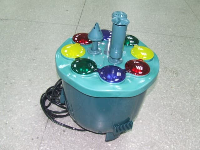
Apr 11, 2007Toba Magic Fountain
Equipment Class
CYY - Communications Receiver used w/Pt 15 Transmitter