UEK104133Vehicle mounted GPS Receiver with CDMA Transceiver
Eia Electronics NV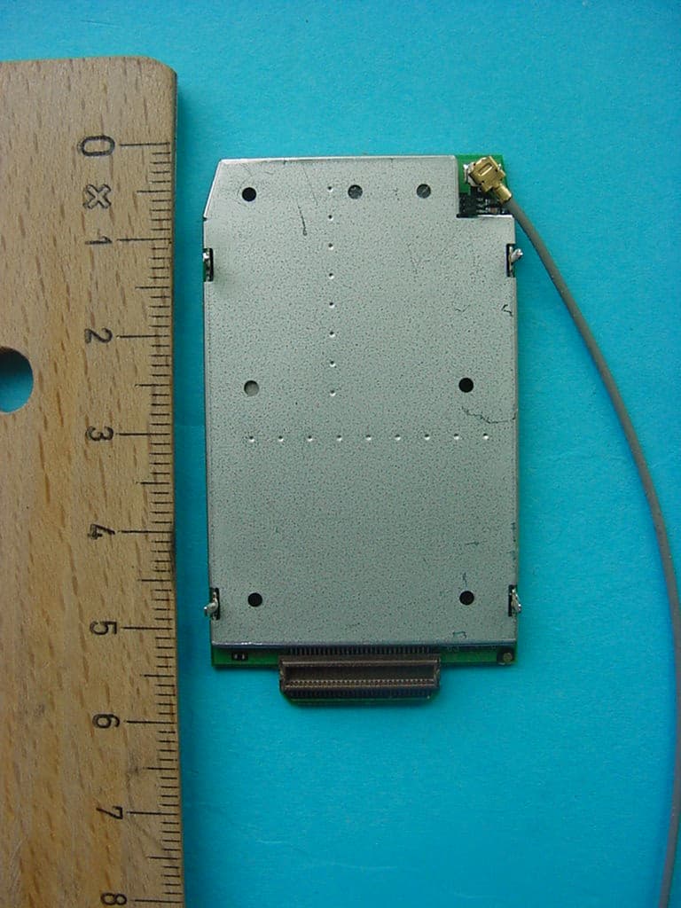
Click to zoom
Application Details
- Equipment Class
- PCB - PCS Licensed Transmitter
- Date of Grant
- Sep 07, 2006
- Application Purpose
- Original Equipment
- Date of Application
- Sep 07, 2006
- Equipment Note
- Vehicle mounted GPS Receiver with CDMA Transceiver
- Frequency Range
- 824.70000000 - 848.31000000
- Company
- Eia Electronics NV
- Country
- Belgium
Documents & Files
Document Text
Text extracted from the exhibit documents filed with the FCC. Open a document above to read the original.
Users Manual
EIA Electronics Integrated Electronic Solutions for OEMs Installation manual TRC810-4CG EIA Electronics Installation manual TRC810-4CG 1/11 Table of Contents Table of Contents.....................................................................................................................1 Table of figures and tables......................................................................................................1 Conventions..............................................................................................................................2 1.1 Mounting holes........................................................................................................2 1.2 Main Connector.......................................................................................................3 1.3 Wireless modem and GPS antenna........................................................................3 2 Connectors.......................................................................................................................4 2.1 Main Connector.......................................................................................................4 2.2 Wireless modem antenna connector SMA-type....................................................6 2.3 Gps antenna connector MCX-type.........................................................................6 3 Replacing the Li-ion battery...........................................................................................6 4 Mounting the back panel.................................................................................................8 5 Additional installation hints............................................................................................9 5.1 Mounting on a frame...............................................................................................9 5.2 Fusing.......................................................................................................................9 5.3 Antenna....................................................................................................................9 5.4 Wiring harness.........................................................................................................9 6 Warnings and Statements..............................................................................................10 Table of figures and tables Figure 1: Mounting holes........................................................................................................2 Figure 2: Main connector........................................................................................................3 Figure 3: Wireless modem antenna connector.......................................................................3 Figure 4: GPS antenna connector...........................................................................................4 Figure 5: Frontal view of main connector with indication of pin 1......................................4 Figure 11: Position of the battery inside the housing............................................................6 Figure 12: Disconnecting the li-ion battery...........................................................................7 Figure 13: Mounting the back panel.......................................................................................8 Table 1 : Pin names and their descriptions.............................................................................5 EIA Electronics Installation manual TRC810-4CG 2/11 Conventions 1.1 Mounting holes The mounting holes are predestined to be used with a Metric8 bolt. Figure 1: Mounting holes EIA Electronics Installation manual TRC810-4CG 3/11 1.2 Main Connector The main connector is an AMP-Tyco Superseal 5-1447223-7 Mating part is AMP-Tyco Superseal 2-1447232-6 Figure 2: Main connector 1.3 Wireless modem and GPS antenna. Figure 3: Wireless modem antenna connector EIA Electronics Installation manual TRC810-4CG 4/11 Figure 4: GPS antenna connector 2 Connectors 2.1 Main Connector Frontal view of connector with indication of pin 1 etc Figure 5: Frontal view of main connector with indication of pin 1 EIA Electronics Installation manual TRC810-4CG 5/11 pin numbernamedescription 1PBATcontinuous power supply(+battery) 2Pkeyafter contact input(ignition) 3output1high side output 4output2high side output 5output3high side output 6output4high side output 7multi_in1configurable input 8multi_in3configurable input 9multi_in5configurable input 10multi_in7configurable input 11multi_in9configurable input 12tx1RS232 tx signal channel 1 13cts1RS232 cts signal channel 1 14dtr1RS232 dtr signal channel 1 15ri1RS232 ri signal channel 1 16tx2RS232 tx signal channel 2 17cts2RS232 cts signal channel 2 18dtr2RS232 dtr signal channel 2 19ri2RS232 ri signal channel 2 20rs232-rxRS232 rx signal proprietary channel 21canl-1Can low channel 1 22canl-2Can low channel 2 23output_powerpower supply for high side outputs 24output_powerpower supply for high side outputs 25output_powerpower supply for high side outputs 26groundground connection 27groundground connection 28groundground connection 29multi_in2configurable input 30multi_in4configurable input 31multi_in6configurable input 32multi_in8configurable input 33multi_in10configurable input 34rx1RS232 rx signal channel 1 35rts1RS232 rts signal channel 1 36dsr1RS232 dsr signal channel 1 37cd1RS232 cd signal channel 1 38rx2RS232 rx signal channel 2 39rts2RS232 rts signal channel 2 40dsr2RS232 dsr signal channel 2 41cd2RS232 cd signal channel 2 42rs232-txRS232 rx signal proprietary channel 43canh-1Can high channel 1 44canh-2Can high channel 2 Table 1 : Pin names and their descriptions EIA Electronics Installation manual TRC810-4CG 6/11 2.2 Wireless modem antenna connector SMA-type See Figure 3 for the positioning on the back plane of the SMA connector. When facing the back panel the SMA connector is situated on the right. The antenna cable must be locked by screwing the…
Text truncated - open the document above for the full version.
ID Label/Location Info
Label and Label position. The label is located on the bottom side of the TRC810-4CG. Trade Name: EIA Electronics NV Model No: TRC810-4CG This device complies with Part 15 of the FCC Rules and with RSS-210 of Industry Canada. Operation is subject to the following two conditions. (1) this device my not cause harmful interference, and (2) this device must accept any interference received, including interference that may cause undesired operation. FCC ID: UEK104133 IC: 6630A-104133
RF Exposure Info
CETECOM ICT Services GmbH Untertürkheimer Str. 6-10, 66117 Saarbruecken Phone: +49 (0) 681 598-0 Fax: -9075 RSC-Laboratory Phone: +49 (0) 681 598-0 Fax: -9075 Test report No.: 2-4372-01-02/06 Date: 2006-07-14 Page 77 of 81 4 MPE Calculation These equations are generally accurate in the far field of an antenna but will over predict power density in the near field, where they could be used for making a “worst case” prediction. S = PG/4πR 2 where S = power density ( in appropriate units, e.g. mW/cm 2 ) P = power input to the antenna (in appropriate units e.g. mW) G = power gain of the antenna in the direction of interest relative to the isotropic radiator R = distance to the center of radiation of the antenna (appropriate units e.g. cm) Or S = EIRP/4πR 2 where EIRP = equivalent isotropically radiated power Calculation: (CDMA 850) Calculation: (CDMA 1900) (Calculated for max. EIRP) EIRP: 24.7dBm +2,14 dBi = 493.1 mW EIRP: 28.3 dBm = 676.1 mW calculated at distance of 20 cm: power density = 493.1 /4π20 2 = 0.098 mW/ cm 2 power density = 676.1/4π20 2 = 0.135 mW/ cm 2 Limit: 1mW/ cm 2 is the reference level for general public exposure according to the OET Bulletin 65, Edition 97-01 Table 1.
Test Report
CETECOM ICT Services GmbH Untertürkheimer Str. 6-10, 66117 Saarbruecken Phone: +49 (0) 681 598-0 Fax: -9075 RSC-Laboratory Phone: +49 (0) 681 598-0 Fax: -9075 Test report no.: 2-4372-01-02/06 Date: 2006-07-14 Page 1 of 81 Recognized by the Federal Communications Commission Anechoic chamber registration no.: 90462 (FCC) Anechoic chamber registration no.: 3463 (IC) TCB ID: DE 0001 Accredited by the German Accreditation Council DAR–Registration Number DAT-P-176/94-D1 Independent ETSI compliance test house ETSI Accredited Bluetooth ® Test Facility (BQTF) Test report No. : 2-4372-01-02/06 Applicant : EIA Electronics NV Type : TRC810-4CG Test Standard : FCC Part 22, 24 RSS-129, -133 FCC ID : UEK104133 Certification No. IC : 6630A-104133 The Bluetooth word mark and logos are owned by the Bluetooth SIG, Inc. and any use of such marks by Cetecom ICT is under license CETECOM ICT Services GmbH Untertürkheimer Str. 6-10, 66117 Saarbruecken Phone: +49 (0) 681 598-0 Fax: -9075 RSC-Laboratory Phone: +49 (0) 681 598-0 Fax: -9075 Test report No.: 2-4372-01-02/06 Date: 2006-07-14 Page 2 of 81 Table of contents 1 GENERAL INFORMATION ................................................................................................................................... 3 1.1. ADMINISTRATIVE DATA OF THE TEST FACILITY..................................................................................................... 3 1.1.1 Identification of the testing laboratory ......................................................................................................... 3 1.2. NOTES................................................................................................................................................................... 3 1.3 DETAILS OF APPLICANT......................................................................................................................................... 4 1.4 APPLICATION DETAILS.......................................................................................................................................... 4 1.5 TEST ITEM............................................................................................................................................................. 5 1.6 TEST SETUP........................................................................................................................................................... 6 1.7 TEST STANDARDS.................................................................................................................................................. 6 2 STATEMENT OF COMPLIANCE .......................................................................................................................... 7 2.1 SUMMARY OF MEASUREMENT RESULTS................................................................................................................ 7 2.1.1 CDMA 1900 .................................................................................................................................................. 7 2.1.2 CDMA 850 .................................................................................................................................................... 7 3 MEASUREMENTS AND RESULTS ....................................................................................................................... 8 3.1 PART PCS 1900 ................................................................................................................................................... 8 3.1.1 RF Power Output .......................................................................................................................................... 8 3.1.2 Frequency Stability..................................................................................................................................... 12 3.1.3 Radiated Emissions..................................................................................................................................... 15 3.1.4 Receiver Radiated Emissions ...................................................................................................................... 25 3.1.5 Conducted Spurious Emissions ................................................................................................................... 29 3.1.6 Block Edge Compliance .............................................................................................................................. 33 3.1.7 Occupied Bandwidth................................................................................................................................... 36 3.2 PART CDMA 850............................................................................................................................................... 43 3.2.1 RF Power Output ........................................................................................................................................ 43 3.2.2 Frequency Stability..................................................................................................................................... 46 3.2.3 Radiated Emissions..................................................................................................................................... 49 3.2.4 Receiver Radiated Emissions ...................................................................................................................... 59 3.2.5 Conducted Spurious Emissions ................................................................................................................... 63 3.2.6 Block Edge Compliance .............................................................................................................................. 67 3.2.7 Occupied Bandwidth................................................................................................................................... 70 4 MPE CALCULATION ...........................................................…
Text truncated - open the document above for the full version.
Test Setup Photos
CETECOM ICT Services GmbH Untertürkheimer Str. 6-10, 66117 Saarbruecken Phone: +49 (0) 681 598-0 Fax: -9075 RSC-Laboratory Phone: +49 (0) 681 598-0 Fax: -9075 Annex to Test report no.: 2-4372-01-02/06 Date: 2006-07-19 Page 20 of 32 Photo 2 (Radiated Emissions): CETECOM ICT Services GmbH Untertürkheimer Str. 6-10, 66117 Saarbruecken Phone: +49 (0) 681 598-0 Fax: -9075 RSC-Laboratory Phone: +49 (0) 681 598-0 Fax: -9075 Annex to Test report no.: 2-4372-01-02/06 Date: 2006-07-19 Page 21 of 32 Photo 3 (Radiated Emissions):
Contact Information
Applicant
Dirk Wiese(Technical Director)
Test Firm
cetecom advanced GmbHGerald Schmidt
Technical Specifications
| # | Rule Parts | Frequency Range | Power Output | Emission | Tolerance |
|---|---|---|---|---|---|
| 2 | 22H | 824.7 MHz - 848.31 MHz | 295.00 mW | 1M25F9W | 0.0129 ppm |