UOKVSUNGPSTRACKERGSM/GPRS Module
ShenZhen V-Sun Electronics Co., Ltd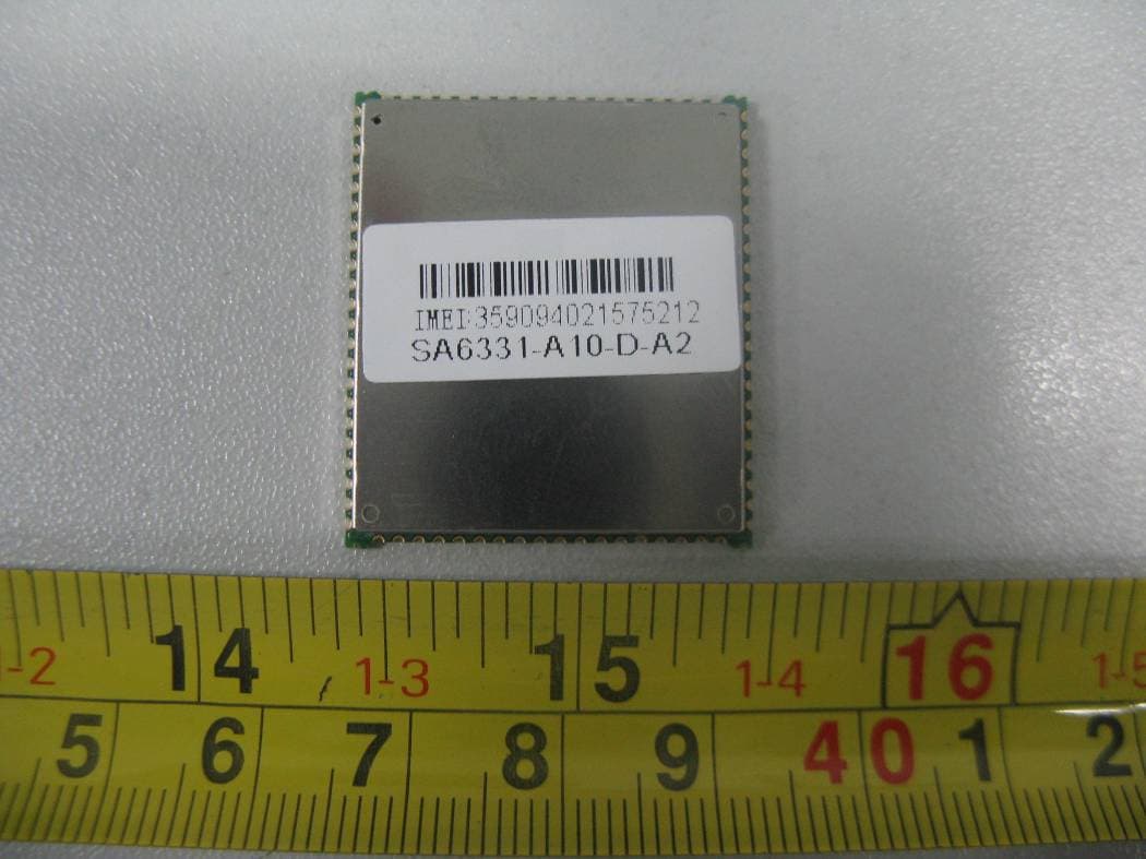
Click to zoom
Application Details
- Equipment Class
- PCB - PCS Licensed Transmitter
- Date of Grant
- Nov 06, 2010
- Application Purpose
- Original Equipment
- Date of Application
- Nov 06, 2010
- Equipment Note
- GSM/GPRS Module
- Frequency Range
- 1850.20000000 - 1909.80000000
- Country
- China
Documents & Files
Document Text
Text extracted from the exhibit documents filed with the FCC. Open a document above to read the original.
Users Manual
1 V3338 USER MANUAL 2 Document Name: V3338 specification Version: 01.04 Date : 2009 -11 -12 Status : Draft General Notes UFT offers this information as a service to its customers, to support application and engineering efforts that use UFT products. The information provided is based upon requirements specifically provided to UFT by the customers. UFT has not undertaken any independent search for additional relevant information, including any information that may be in the customer’s possession. Furthermore, system validation of this UFT product within a larger electronic system remains the responsibility of the customer or the customer’s system integrator. All specifications supplied herein are subject to change. Important Notes Operation is subject to the following (1) This device may not cause harmful interference, and (2) this device must accept any interference received, including interference that may cause undesired operation. Changes or modifications not expressly approved by the party responsible for compliance could void the user's authority to operate the equipment. Copyright This document contains proprietary technical information which is the property of UFT Limited., copying of this document and giving it to others and the using or communication of the contents thereof, are forbidden without express authority. Offenders are liable to the payment of damages. All rights reserved in the event of grant of a patent or the registration of a utility model or design. All specification supplied herein are subject to change without notice at any time. Copyright © UFT Limited. 2008 two conditions: FCC Radiation Exposure Statement: This equipment complies with FCC radiation exposure limits set forth for uncontrolled environment . This equipment should be installed and operated with minimum distance 20cm between the radiator& your body. 3 Contents Contents ..................................................................................................................................................... 3 0 Version History ................................................................................................................................... 4 1 Introduction ........................................................................................................................................ 5 1.1. Related documents ................................................................................................................. 5 2. Product concept .................................................................................................................................. 6 2.1. V3338 features at a glance .................................................................................................... 6 3. Hardware Interface ............................................................................................................................. 7 3.1. Module Interface .................................................................................................................... 7 3.2. Pin description ........................................................................................................................ 7 3.3. Operating modes .................................................................................................................... 9 3.4. Power supply ........................................................................................................................ 10 3.5. Power up and power down scenarios ................................................................................... 11 3.5.1. Turn on V3338 ........................................................................................................ 11 3.5.2. Turn off V3338 ....................................................................................................... 12 3.5.3. Hardware Shut Off V33 38 ...................................................................................... 12 3.5.4. Power saving ............................................................................................................ 12 3.6. Serial interfaces .................................................................................................................... 12 3.7. Audio interfaces ................................................................................................................... 13 3.8. DAI PCM Interface .............................................................................................................. 14 3.9. PWM and Alerter (needs software support) ......................................................................... 15 3.10. Antenna ................................................................................................................................ 15 3.11. SIM card interface ................................................................................................................ 16 3.12. Keypad Interface .................................................................................................................. 18 3.13. LCD Interface (Parallel display can not work onV3338) ............................................... 19 3.14. RTC backup .......................................................................................................................... 21 3.15. IOs ........................................................................................................................................ 21 3.16. External Interrupt ................................................................................................................. 21 3.17. Open-Drain Output Swith .................................................................................................... 22 3.18. ADC ..................................................................................................................................... 22 3.19. Digital Pin Electrical Characteristics ............................…
Text truncated - open the document above for the full version.
Block Diagram
RF ANT 824~894MHz 890~960MHz 1710~1880MHz 1850~1990MHz PA SKY77518 FLASH MT6223 AD6548 SAW Filter
External Photos
EXHIBIT B - EUT EXTERNAL PHOTOGRAPHS EUT – Top View EUT – Rear View EUT on the Test Supported Board View
ID Label/Location Info
EXHIBIT A - FCC ID LABELING AND LOCATION FCC ID Label FCC ID Label Location Label here The label shown shall be permanently affixed at a conspicuous location on the device and be readily visible to the user at the time purchase (Labeling requirements per 2.925)
Internal Photos
EXHIBIT C - EUT INTERNAL PHOTOGRAPHS EUT – PCB Board Shielded off View EUT – PCB Board Bottom View
Operational Description
Circuit Description GSM moduleV3338 is composed of three parts, which are radio frequency parts, the CPU part and the interface part. RF section RF part of the module consists of three parts, AD6548, SKY77518, and SAW Filters. The RF signal is include receive signal and sends signal. Modules receiving the signal from the antenna then separate the send and receive signals by the internal antenna switch of R18 SKY77518. The received signals input the pin 11 of R18, then feet out into the receiver front-end circuit from the pin6 and pin7 of R18. The working status of R18 is controlled by the CPU signals PAEN, BANDSW_DCS, VAPC, and VCXOEN. After the RF antenna switch inside the R18, two analog switches U102, U103 also will be used to separate the 850/900 and 1800 /1900 signals. Four Saw filter U2, U506, U507, U3 will be pass before the 850, 900, 1800, 1900 signals enter into the AD6548. After the processing of AD6548, signals will into the CPU. About the sending signals which processed by the CPU will be send into the AD6548, then feet into the power amplifier SKY77518 by the pin10 and pin11 of AD6548, the amplified signal sent by the antenna from the pin 11 of SKY77518. CPU part Based on a dual-processor architecture, MT6223 integrate both an ARM7EJ-S core and 2 digital signal processor cores. ARM7EJ-S is the main processor that is responsible for running 2G and 2.5G protocol software. Digital signal processors handle the MODEM algorithms as well as advanced audio functions. Except for some mixed-signal circuitries, the other building blocks in MT6223 are connected to either the microcontroller or one of the digital signal processor. The interface of MT6223 control radio consists of Baseband Serial Interface (BSI), Baseband Parallel Interface (BPI), Automatic Power Control (APC) and Automatic Frequency Control (AFC) together with APC-DAC and AFC-DAC. MT6223 also consist of the following subsystems: Microcontroller Unit (MCU) Subsystem Digital Signal Processor (DSP) Subsystem MCU/DSP Interface Microcontroller Peripherals Microcontroller Coprocessors DSP Peripherals Voice Front End Audio Front End Baseband Front End Timing Generator Power, Reset and Clock subsystem LDOs, Power-on sequences, switches and SIM level shifters. Interface Section The interface of V3338 includes the GPIO, UART, SIM Interface, POWER, AUDIO, RF Pad. The pins of AUDIO, GPIO, UART, SIM Interface are directly connect to the TP1. Between the RF antenna pad and the pin 11 of SKY77518 are connected by the capacitor C7. The POWER pins are directly power supply the R18, TP1.
Parts List/Tune Up Info
Turn On Procedure of GSM Module For test the V3338 module, you need solder the V3338 to your application board or our EVB. The basic procedure of turn on V3338 need these steps : 1. Install a Dual band or Quad band GSM RF antenna 2. Insert SIM Card 3. Power on pin 35,53,54 of V3338 with 3.8V 4. Connect pin 44 to GND not less than 3 second then disconnect 5. After the V3338 power on, you could do test on the module V3338
Parts List/Tune Up Info
Item Qty Order Part NumDescription 1 1 GRM1555C1H1R5CZ01CAP-0402-NPO-1.5pF-50V±0.25pF 2 4 GRM1555C1H6R0CZ01DCAP-0402 6p 50V,C0G 3 2 GRM1555C1H8R0CZ01DCAP-0402 8p 50V,C0G 4 2 GRM1555C1H120JZ01DCAP-0402 12p 50V,C0G 5 4 GRM1555C1H180JZ01DCAP-0402-NPO-18pF-50V±5% 6 2 GRM1555C1H220JZ01DCAP-0402,22PF,50V,NPO 7 1 GRM1555C1H270JZ01CAP-0402,27PF 50V,C0G 8 6 GRM1555C1H330JZ01CAP-0402 5% 33p/50V COG 9 2 GRM1555C1H101JZ01CAP-0402,5%,50V,COG,100p 10 1 GRM1555C1H221JA01DCAP-0402,220p 50V,COG 11 2 GRM155R71H103KA01CAP-0402,10nF 50V, X7R 12 1 GRM155R71C473KA01DCAP-0402,47n 16V,X7R 13 21 GRM155R71C104KA88CAP-0402 10%,10v,X5R,100n 14 5 GRM155R60J105KE19CAP-0402,1UF 10V,X5R 15 7 GRM188R60J205KA01DCAP-0603 10% 2uF/6.3V X5R 16 1 F920J226MPACAP-0805-TAN-22uF-6.3V±20% 17 14 RC0402JR-070RLRES-0402-0ohm±5%-1/10W 18 1 RL0805FR-7W0R2LRES-0805-0.2ohm±1%-1/4W 19 8 RC0402JR-071KLRES-0402-1Kohm±5%-1/16W 20 3 RC0402JR-071K5LRES-0402-1.5Kohm±5%-1/17W 21 1 RC0402JR-074K7LRES-0402-4.7Kohm±5%-1/16W 22 1 RC0402JR-0722KLRES-0402-22Kohm±5%-1/16W 23 1 RC0402JR-07100KL RES-0402-100Kohm±5%-1/16W 24 1 RC0603JR-070RLRES-0603-0ohm±5%-1/10W 25 2 LQG15HS1N8S02DIND-0402, 1.8nH 5% 26 1 LQG15HS2N7S02CAP_NPA,2.7nH 27 1 LQG15HS4N7S02CAP_NPA,4.7nH 28 1 LQG15HS5N8S02DIND-0402-5.8nH±5% 29 2 LQG15HS18NJ02DIND-0402,18nH 5% 30 1 LQG15HS27NJ02DIND-0402,27nH 5% 31 4 ICVN0505X150FRICVN0505X150FR 32 1 Q13MC146100020032.768KHZ-12.5PF 33 1 K5L6331CAA-D270K5L6331CAA-D270 34 1 MT6223DA/AMT6223D 35 1 FAR-F5KB-942M50-B4EBFAR-F5KB-942M50-B4EB 36 1 FAR-F5KB-881M50-B4EAFAR-F5KB-881M50-B4EA 37 1 FAR-F6KB-1G8425-B4GAFAR-F6KB-1G8425-B4GA 38 1 FAR-F6KB-1G9600-B4GB FAR-F6KB-1G9600-B4GB 39 1 SKY77518-21RF PA 40 2 AS179-92LFAS179 41 1 ME-RF-SHIELD-HOLDER-Q- V3338 Shielding Case 42 1 ME-RF-SHIELD-COVER-V3338 Shielding Case 43 1 CMT-V3338A-041-V1PCB 44 2 1SS400TE61 45 1 GRM1555C1H470JZ01DCAP_0402B 47pF 46 2 GRM1555C1H820JZ01DCAP_0402B 82pF 47 4 RC0402JR-072K2LR_0402B 2.2K 48 1 RC0402JR-0751RLR_0402B 51ohm 49 1 AD6548BCPZ-RL3/CAD6548 50 2 RC0402JR-0782RL IND-0402-82ohm±5% 51 1 X1E000021031400 CRYSTAL-26MHz LC=8.5pF 3.2x2.5x0.7mm 52 2 GRM1555C1H390JZ01DCAP-0402,39pF 50V,X7R 53 1 GRM155R71C333KA01DCAP-0402 10%,16v,X7R,33nF 54 1 GRM155R61A224KE19CAP-0402,10V, X5R 220nF
RF Exposure Info
Shenzhen V-SUN Electronics Co., Ltd. FCC ID: UOKVSUNGPSTRACKER Report No.: RSZ10101805-22H&24E Page 8 of 29 FCC Part 22H/24E Test Report FCC §1.1307 & §2.1091 - RF EXPOSURE Applicable Standard According to §1.1307(b)(1), systems operating under the provisions of this section shall be operated in a manner that ensures that the public is not exposed to radio frequency energy level in excess of the Commission’s guidelines. According to §1.1310 and §2.1091 RF exposure is calculated. Limits for General Population/Uncontrolled Exposure Limits for General Population/Uncontrolled Exposure Frequency Range (MHz) Electric Field Strength (V/m) Magnetic Field Strength (A/m) Power Density (mW/cm 2 ) Averaging Time (minutes) 0.3-1.34 614 1.63 *(100) 30 1.34-30 824/f 2.19/f *(180/f 2 ) 30 30-300 27.5 0.073 0.2 30 300-1500 / / f/1500 30 1500-100,000 / / 1.0 30 f = frequency in MHz * = Plane-wave equivalent power density Test Data Predication of MPE limit at a given distance Where: S = power density (in appropriate units, e.g. mW/cm2) P = output power to antenna G= Antenna Gain (numeral) R = distance to the center of radiation of the antenna (appropriate units, e.g., cm) Max Conducted Power Band Frequency (MHz) Ant. Gain (dBi) (dBm) (mW) Duty Cycle Evaluation Distance (cm) Power Density (mW/cm 2 ) MPE Limit (mW/cm 2 ) GSM 850 (4 Slots) 824.2 0 29.56 904 4/8 20 0.0900 0.5495 PCS 1900 (4 Slots) 1850.2 0 28.35 684 4/8 20 0.0681 1.0 Result: EUT meets the mobile 20 cm separation distance as specified in section 2.1091 of the FCC rules. An appropriate RF exposure compliance statement will be placed in the User’s Guide.
Test Report
Note: This test report is prepared for the customer shown above and for the device described herein. It may not be duplicated or used in part without prior written consent from Bay Area Compliance Laboratories Corp. This report must not be used by the customer to claim product certification, approval, or endorsement by NVLAP*, NIST, or any agency of the Federal Government. * This report may contain data that are not covered by the NVLAP accreditation and are marked with an asterisk “*” (Rev.2) FCC PART 22H, 24E MEASUREMENT AND TEST REPORT For Shenzhen V-SUN Electronics Co., Ltd. A1601-1605, Construction Group Building, Hongling Rd, C, Luohu District, Shenzhen, Guangdong, China FCC ID: UOKVSUNGPSTRACKER Report Type: Original Report Product Type: GSM/GPRS Module Test Engineer: Alvin Huang Report Number: RSZ10101805-22H&24E Report Date: 2010-10-29 Reviewed By: Merry Zhao EMC Engineer Prepared By: Bay Area Compliance Laboratories Corp. (Shenzhen) 6/F, the 3rd Phase of WanLi Industrial Building, ShiHua Road, FuTian Free Trade Zone Shenzhen, Guangdong, China Tel: +86-755-33320018 Fax: +86-755-33320008 Shenzhen V-SUN Electronics Co., Ltd. FCC ID: UOKVSUNGPSTRACKER Report No.: RSZ10101805-22H&24E Page 2 of 29 FCC Part 22H/24E Test Report TABLE OF CONTENTS GENERAL INFORMATION.......................................................................................................................................4 PRODUCT DESCRIPTION FOR EQUIPMENT UNDER TEST (EUT) .....................................................................................4 OBJECTIVE...................................................................................................................................................................4 RELATED SUBMITTAL(S)/GRANT(S).............................................................................................................................4 TEST METHODOLOGY..................................................................................................................................................4 TEST FACILITY.............................................................................................................................................................4 SYSTEM TEST CONFIGURATION ..........................................................................................................................6 JUSTIFICATION.............................................................................................................................................................6 EQUIPMENT MODIFICATIONS.......................................................................................................................................6 CONFIGURATION OF TEST SETUP.................................................................................................................................6 BLOCK DIAGRAM OF TEST SETUP................................................................................................................................6 SUMMARY OF TEST RESULTS ...............................................................................................................................7 FCC §1.1307 & §2.1091 - RF EXPOSURE..................................................................................................................8 APPLICABLE STANDARD..............................................................................................................................................8 TEST DATA..................................................................................................................................................................8 FCC §2.1047 - MODULATION CHARACTERISTIC ..............................................................................................9 FCC § 2.1046, § 22.913 (A) & § 24.232 (C) - RF OUTPUT POWER......................................................................10 APPLICABLE STANDARDS...........................................................................................................................................10 TEST PROCEDURE......................................................................................................................................................10 TEST EQUIPMENT LIST AND DETAILS.........................................................................................................................10 TEST DATA................................................................................................................................................................11 FCC §2.1049, §22.917, §22.905 & §24.238 - OCCUPIED BANDWIDTH ..............................................................13 APPLICABLE STANDARDS...........................................................................................................................................13 TEST PROCEDURE......................................................................................................................................................13 TEST EQUIPMENT LIST AND DETAILS.........................................................................................................................13 TEST DATA................................................................................................................................................................13 FCC §2.1051, §22.917(A) & §24.238(A) - SPURIOUS EMISSIONS AT ANTENNA TERMINALS ..................17 APPLICABLE STANDARDS...........................................................................................................................................17 TEST PROCEDURE......................................................................................................................................................17 TEST EQUIPMENT LIST AND DETAILS.........................................................................................................................17 TEST DATA....................................…
Text truncated - open the document above for the full version.
Test Setup Photos
EXHIBIT D - TEST SETUP PHOTOGRAPHS Below 1 GHz: Radiated Emissions - Front View Below 1 GHz: Radiated Emissions - Rear View Above 1 GHz: Radiated Emissions - Front View Above 1 GHz: Radiated Emissions - Rear View Frequency Stability
Contact Information
Applicant
Guo Dong Wang
Test Firm
Bay Area Compliance Laboratory Corp. (Shenzhen)John Chan
Technical Specifications
| # | Rule Parts | Frequency Range | Power Output | Emission | Tolerance |
|---|---|---|---|---|---|
| 2 | 24E | 1.85 GHz - 1.91 GHz | 1 W | 250KGXW | 2.5 ppm |