UPNLD500UHF Transceiver
Alltronics Tech. Mftg. Limited.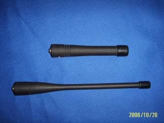
Click to zoom
Application Details
- Equipment Class
- TNF - Licensed Non-Broadcast Transmitter Held to Face
- Date of Grant
- Apr 01, 2007
- Application Purpose
- Original Equipment
- Date of Application
- Apr 01, 2007
- Equipment Note
- UHF Transceiver
- Frequency Range
- 406.10000000 - 470.00000000
- Country
- China
Documents & Files
Document Text
Text extracted from the exhibit documents filed with the FCC. Open a document above to read the original.
Users Manual
User Handbook (INSTRUCTION MANUAL) UHF TRANSCEIVER LD-500 ABOUT CE CE Versions of the LD-500 which display the “CE” symbol on the serial number seal ,comply with the essential requirements of the European Radio and Telecommunication Terminal Directive 1999/5/EC. This warning symbol indicates that this equipment operates in nonharmonised frequency bands and /or may be subject to licensing conditions in the country of use.Be sure to check that you have the correct version of this radio or the correct programming of this radio,to comply with national licensing requirement. INSTALLATION NOTES •SAR compliance for body-worn operations is restricted to belt-clips, holsters or similar accessories that have no metallic component in the assembly and must provide at least 1.5 cm separation between the device and the user’s body." FOREWORD Thank you for purchasing the LD-500 FM transceiver. READ ALL INSTRUCTIONS carefully and completely before using the transceiver. i SAVE THIS INSTRUCTION MANUAL-This instruction manual contains important operating instructions for the transceiver. IMPORTANT CAUTION! NEVER hold the transceiver so that the antenna is very close to,or touching exposed parts of the body, especially the face or eyes,while transmitting.The transceiver will perform best if the microphone is 5 to 10 cm away from the lips and the transceiver is vertical. CAUTION! NEVER operate the transceiver with a headset or other audio accessories at high volume levels. CAUTION! NEVER short the terminals of the battery pack.. DO NOT push the PTT when not actually desiring to transmit. AVOID using or placing the transceiver in direct sunlight or in areas with temperatures below -10 or above +50 . The basic operations,transmission and reception of the transceiver,are guaranteed within the specified operating temperature range (depending on version). DO NOT modify the transceiver for any reason. KEEP the transceiver from the heavy rain,and Never immerse it in the water. The transceiver construction is water resistant,not water proof. The use of non-lcom battery packs/chargers may impair transceiver performance and invalidate the warranty. The device may only be used in an occupational environment The transmitter frequencies can only be programmed in the factory and that the user of the device cannot change the frequencies programmed into the device ii Professional TABLE OF CONTENTS ABOUT CE................................................................................................. INSTALATION NOTES............................................................................ FOREWORD.........................................................................................- IMPORTANT.............................................................................................. TABLE OF CONTENTS............................................................................ 1 ACCESSORIES........................................................... ............................1 2 PANEL DESCRIPTION.......................................................................2-3 ■Switches,controls,keys and connectors....................................................3 3 BATTERY PACKS.......................................................................... .....4-7 ■Battery pack replacement................................................................. ........4 ■Battery cautions................................................................................. .......5 ■Battery charging............................................. .................................... .....6 ■Charging NOTE............................................ ..................................... ......7 4 PROGRAMMABLE FUNCTIONS............................................... .... 8-11 5 CONVENTIONAL OPERATION.................................................... 12-14 ■Receiving and transmitting.................................................................. ...12 ■Call procedure........................................................................ .................13 ■Transmitting notes............................................................................ .......14 6 CLONING..................................................................................................15 7 OPTIONS..............................................................................................16-17 ■Options................................................................... ............................16-17 iii ACCESSORIES 1 ■ Accessory attachment Supplied accessories The transceiver comes supplied with the following accessories. Flexible antenna (may differ according to version) Belt clip Antenna The antenna screws onto the transceiver as illustrated right. 1 2 PANEL DESCRIPTION ■ Switches, controls,keys and connectors PANEL DESCRIPTION 2 n ROTARY SELECTOR [SEL] Selects operating channel,or bank, depends on setting. o DEALER-PROGRAMMABLE KEY [F0 (Red)] p ANTENNA CONNECTOR Connects the supplied antenna. q PTT SWITCH [PTT] Push and hold to transmit;release to receive. r Microphone s DEALER-PROGRAMMABLE KEYS [F2(Black)],[F3 (Black)] •Push to select the operating channel. •Can be programmed as []/[#].(SmarTrunk mode only) t VOLUME CONTROL [VOL] Turns power ON and adjusts the audio level. u TRANSMIT/BUSY INDICATOR Lights red while transmitting;lights green while receiving a signal, or squelch is open. v MULTI CONNECTOR Connect optional speaker-microphone,etc.. a Speaker 3 BATTERY PACKS 3 ■ Battery pack replacement Before replacing the battery pack, the volume control MUST be rotated fully counterclockwise, until a click is heard,to turn the power OFF. • Slide the battery release forward,then pull the battery pack upward with the transceiver facing you. BATTERY PACKS Charging period Battery pack Voltage Capacity BC-137 BC-119 or BC-121 with AD-94 Battery life* BP-208 Battery case for AA(R6) X6 alkaline N/A N/A __ BP-209 7.2V 1100 mAh15 hrs. 1.5 hrs. 7 hrs. BP-210 …
Text truncated - open the document above for the full version.
Block Diagram
LPF ANTCONNECTOR D101/D102/D103 ANT SW Block Diagram BPF T201 RF AMP T202 1st MIX 21.7MHz CRYSTAL BPF 1st IF AMP T215 BPF T107 TX POWER AMP T101/T102/T105 TX YOUNGER T321/T322/T323 VCO PLL U401LMX2332 RF INPUT PLL DET POWER CONTROL BUFF AMP CMX808 SQUELCHCONTROL WITH HYSTERSIS SQUELCH TRIGGER 2nd MIX NOISE AMP 2nd IF AMP DETECTOR F.M. 450KHz CERAMIC FILTER U240/TA31136 CMX808 U621 LM386 AUDIO BUFF AMP AUDIO POWER AMP VOL SPEAKER CR24021.250MHz SQCK DATA STB MCUEM78P451AQ POWER SUPPLYVoltage control V-TX V-RX V-VCO MONI PTT + - LM4558 U601 AUDIO LIMIT AMP + - VCC MIC AMPU601A LM4558 U701/LM2904 MIC U831 Regulator +5V POWER SW VB7 2V 1 2 3 45 6 12 34 5 6 Text D A BC Text D CBA Title Size B Number Revision Date: 13-Sept-2006 Sheet of Drawn By: SW-DIP4 CR2 TCXO 14.4MHZ Battery
Cover Letter(s)
Applicant ATTESTATION Subject: Channel Frequency To whom it may concern: We Alltraonics Tech. Mftg. Limited , the undersigned, hereby attestation that the LD-500 transmitter frequencies can only be programmed in the factory and that the user of the device cannot change the frequencies programmed into the device. Sincerely yours, Signature: Typed or Printed Name: Eddy Ngai Title: RD Manager Company Name: Alltraonics Tech. Mftg. Limited
External Photos
APPENDIX III External Photos EUT – Front View EUT – Rear View EUT – Top View EUT – Antenna View Antenna 1 Antenna 2
ID Label/Location Info
APPENDIX I FCC ID Label FCC ID: UPNLD500
ID Label/Location Info
APPENDIX II FCC ID Label Location FCC ID Label Location
Internal Photos
APPENDIX IV Internal Photos Main Board – Uncovered View-1 Main Board – Uncovered View-2 Main Board – Components View Main Board –Components View(1) Main Board –Components View (2)
Operational Description
LD-500 Antenna specification Antenna 1: Frequency Range: 400MHz-470MHz, Gain: 0.89dBi Connector: SMA Length:141mm Antenna 2: Frequency Range: 400MHz-470MHz, Gain: 0.79dBi Connector: SMA Length:80mm
Operational Description
Circuit Description The received RF signal from antenna is filtered by a complex low pass filter build-up by L118 L114 C154 L113 C151 L112 C149 C153 C150 C147C142 and RF switch by D101 D102 D103 and also Band Pass Filter by L110 C144 L203 L202 C204. This LPF filter also acts as transmitter filter to suppress spurious image frequency. After filtering, received RF signal is amplified by a LNA circuit comprise of MOSFET 3SK240 (T201) that gives 18dB gain and act as a band pass filter. This amplifier is working on switch mode, Controlled by T861 (DTA114YE) open only during received time. The amplified RF signal is coupled by the CAP C211C212 to the first Mixer(T202:3SK240).The first OSC signal is provided by VCO build-up by T321T322T323,The 21.7MHZ signal from mixer is sent to crystal filter FLFL231.After filtering, it is sent to IF amplifier T215.The amplified IF signal is sent to TA31136 IF_IN port. Please refer TA31136 datasheet for more on-TA31136 details. The demodulated signal is output from TA31136 Pin9.This Signal is Coupled by C253 and through CMX808AE3 Send to audio Power amplifier LM386.After amplified, The AF signal drive the Speaker.CMX808AE3 decoded the CTCSS and output control signal to MCU. 1 1 Transmit RF Signal is output from VCO build-up by T321 T322 T323,coupled by C341 and through T341T102T101T105T107 Send to Band Pass Filter.U701(LM2904V) is used for controlling RF power.T107 is RF power amplifier.T105 T101T102 is RF power younger amplifier. Transmit audio signal is picked up by microphone and send to U601,U601 and CMX808AE3 ConstructedU601 and CMX808AE3 is a transmitter audio amplifier and audio filter compander circuit and buffer, improving both signal to noise ratio and frequency response. This transmitter audio signal and CTCSS that CMX808AE3 encoded is send to VCO by E503R504VR521R304C304R305. The base-band use the EM78P451AQ MCU.U401 and CMX808AE3 is controlled by the MCU. The MCU provided the CKDATALE digital signal for wanting frequency and detected CTCSS signal 2 2
Parts List/Tune Up Info
1 4 REMARK 1 1 CHANNEL 2 10K 1 VR 3 / 4.000MHZ, HC-49S 1 CR901 4 / 21.700MHZ,UM-5 2 FL230, FL231 5 / 21.250MHZ, UM-5 1 CR240 6 / 450E,6dB+/-7.5K 1 FL240 7 / speaker 1 8 / MIC 1 MIC601 9 1 SW922(PTT) 10 1 SW923 11 IC / XC6201P502TH TO-92 1 U831 12 Stero phone jack 5PIN 1 jk60113 Stero phone jack 5PIN 1 jk62114 / MWTRANS5 450# 1 TR240 15 / CHIP 6P, +/-5%, 125C, 0603,10V,TAPE 3 C209, C213, C345 16 / CHIP 7P, +/-5%, 125C, 0603,10V,TAPE 2 C108, C136 17 / CHIP 0.1UF, +/-20%, 125C, 0603 ,50V,TAPE 22 C113,C131,C156,C243,C250,C252,C304,C405,C421,C501,C505,C506,C611,C863,C871,C872,C502,C248, C601, C623,C721,C841 18 / CHIP 1UF, +/-20%, 125C, 0603 ,10V,TAPE 1 C253 19 / CHIP 1UF, +/-20%, 125C, 0805,10V,TAPE 3 C126,801, C803 20 / CHIP 0.22uF, +/-20%, 125C,0603,10V,TAPE 1 C251 21 / T.CAP,0.1UF,+/-20% 125C A ,10V,TAPE 2 E403, E503 22 / T.CAP 1UF +/-20%, 125C A ,10V,TAPE 4 E402, E502, E501, E620 23 / T.CAP 2.2UF +/-20% 125C A 10V,TAPE 1 E603 24 / T.CAP 10UF +/-20% 125C A 10V TAPE 6 E240, E404, E504, E621, E831, E832 25 / T.CAP 220UF +/-20% 125C C 6.3V TAPE 1 E622 26 / T.CAP 4.7UF +/-20% 125C, A ,10V,TAPE 4 E321, E601, E602, E701 27 / 3P~10P NPO+/-300PPM/ -25 ~85 2 VC201, VC202 28 / SOD-523 PMSD4148 2 D320, D401 29 / SOD-323 MA77(MA2Z077) 1 D310 30 / SOD-523 HSC277 4 D102, D103, D341, D342 31 / DI ISS356 1 D101 32 / SOD-323 ISV270 3 D301, D302, D303 33 / SOD-106 ISR154-400 1 D801 34 / SOT-323 ISS372 1 D601 35 / GREEN SMD 0603 1 D821 36 / RED SMD 0603 1 D822 2 4 REMARK 37 / R1206,FUSE,2A 1 FR801 38 IC / LMX2332ATM TSSOP20 1 U401 39 IC / LM2904V SSOP8 1 U701 40 IC / LM393 SOP8 1 U881 41 IC / LM4558 SOP8 1 U601 42 CPU / EMC78P451AQ SMD 44PIN QFP 1 U90143 IC / SOP8 24C08 1 U911 44 IC /TA31136FN SSOP16-P-225-0.65B 1 U240 45 IC / LM386-3 SOP8 1 U621 46 IC / TSSOP20 CMX808AE3 1 U501 47 / 2.2nH, 0603, 1 L119 48 / 100nH, 0603, 6 L103, L301, L401, L323, L601,L621 49 / 100nH, 0805, 3 L105, L107, L801 50 / 18nH, 0603, +/-5%, 4 L208, L322, L341, L101 51 / 180nH, 0603, +/-5%, 1 L321 52 / M33L 0.4*1.5*3T 7 L114, L202, L203, L204, L205, L206, L207 53 / M43L 0.4*1.5*4T 3 L112, L110, L113 54 / MAIL 0.4*1.5*8T 2 L106, L118 55 / 1UH, 1008, +/-5%, 1 L104 56 / 220nH, 0805, +/-5%, 1 L109 57 / 2.2UH, 1008, +/-5%, 1 L209 58 / 27nH +/-5% 0805 1 L320 59 / DTC114EE,SOT-523 5 T701, T702, T812, T821, T822 60 / NPN, SST3904, SOT23 1 T601 61 IC SOT-89 HT7033 1 U90262 / DTA114EE,SOT-523 1 T240 63 / DTA114YE,SOT-523 2 T861, T851 64 / DTC114YE,SOT-523 1 T311 65 / 2K508NV,SOT-23 1 T321 66 / 2SC2712,SOT23 1 T323 67 / 2SC4226,NPN,SOT-323 4 T101, T322, T341, T215 68 / 2SC4988,SOT89 1 T102 69 / 2SK3078,SOT89-ECB 1 T105 70 / 2SK3476,SOT-44 1 T107 71 1 CALL 72 / SOT23 2SB624BV4 2 T811, T871 73 / 3SK177-T1,SOT24 2 T201, T202 74 / 100 -10k +/-25% 0.1W, -55 ~125 ,3*3mm 1 VR521 75 / 100 -50k +/-25% 0.1W, -55 ~125 ,3*3mm 1 VR421 3 4 REMARK 76 TCX0 / 14400.00KHZ 1 CR420 77 PCB 50*110*1.0mm 4 LAYERS FR4,94V-0 178 / CHIP 0.5P, +/-0.25P, 125C, 0603,10V,TAPE 4 C211, C212, C306, C323, 79 / CHIP 1P, +/-0.25P, 125C, 0603,10V,TAPE 9 C135, C147, C154, C149, C205,C213A,C218,C312, C307, 80 / CHIP 1.5P, +/-0.25P, 125C, 0603,10V,TAPE 3 C151, C155, C209A 81 / CHIP 2PF, +/-0.25P, 125C, 0603 ,10V,TAPE 1 C144 82 / CHIP 3P, +/-0.25P, 125C, 0603,10V,TAPE 4 C204, C341, C142, C153 83 / CHIP 4P, +/-0.25P, 125C, 0603,10V,TAPE 2 C148 84 / CHIP 5P, +/-0.25P, 125C, 0603,10V,TAPE 8 C214, C321, C322, C324, C403, C404,C150 C230 85 / CHIP 9P, +/-5%, 125C, 0603,10V,TAPE 1 C111 86 / CHIP 10PF, +/-5%, 125C, 0603 ,10V,TAPE 1 C246 87 / CHIP 100PF, +/-5%, 125C, 0603,10V,TAPE 8 C232, C302, C402, C406, C407, C408,C609 ,C704 88 / CHIP 1NF, +/-10%, 125C, 0603 ,10V,TAPE 21 C116,C119,C123,C206,C207,C208,C210,C254,C310,C311,C328,C401,C503,C600,C610,C804,C422,C521,C605,C706,C707 89 / CHIP 10NF, +/-10%, 125C, 0603 ,10V,TAPE 32 C128,C215,C216,C242,C320,C326,C327,C329,C343,C621,C631,C805,C833,C851,C852,C861,C862,C911,C231,C603,C703,C722,C802,C807,C811,C831,C881,C882,C922,C923,C924,C925 90 / CHIP 22NF, +/-10%, 125C, 0603 ,10V,TAPE 2 C608, C607 91 / CHIP 15P, +/-5%, 125C, 0603,10V,TAPE 2 C203, C217 92 / CHIP 22PF, +/-5%, 125C, 0603,10V,TAPE 3 C240 ,C901, C902 93 / CHIP 22PF, +/-5%, 125C, 0805,10V,TAPE 1 C130 94 / CHIP 220PF, +/-10%, 125C, 0603,10V,TAPE 5 C244, C245, C504, C624 ,C921 95 / CHIP 27PF, +/-5%, 125C, 0603,10V,TAPE 1 C249 96 / CHIP 27NF, +/-10%, 125C, 0603,10V,TAPE 2 C301 ,C604 97 / CHIP 470PF, +/-10%, 125C, 0603,10V,TAPE 24 C106, C107, C109, C110, C114, C120,C121, C125, C129, C138, C143, C145,C157, C305, C344, C346, C247, C602,C615, C702, C705, C832, C941, C606 98 / CHIP 56PF, +/-10%, 125C, 0603,10V,TAPE 1 C241 99 / 15nH, 0603, +/-5%, -55 ~125 , 1/5W 1 L102 100 / CHIP 0 OHM, +/-5%, 1/16W, 0603, TAPE 9 R120, R147, R346, R401, R404, R405,R406, R841, VC301 101 / CHIP 0 OHM, +/-5%, 1/8W, 0805, TAPE 2 R123, R127 102 / CHIP 10 OHM, +/-5%, 1/16W, 0603, TAPE 5 R115, R320, R341, R622,R501 103 / CHIP 100 OHM, +/-5%, 1/16W, 0603, TAPE 11 R204, R208, R209, R240, R321, R323,R921, R631, R821, R922, R926 104 / CHIP 1K, +/-5%, 1/16W, 0603, TAPE 4 R234, R601, R612, L302 105 / CHIP 10K +/-5%, 1/10W, 0603, TAPE 11 R301, R310, R347, R811, R302, R708,R710, R883, R924, R933, R941 106 / CHIP 100K +/-5%, 1/10W, 0603, TAPE 7 R201, R246, R303, R306, R248, R603, R930 107 / CHIP 1.2K, +/-5%, 1/10W, 0603, TAPE 2 R247, R923 4 4 REMARK 108 / CHIP 120K +/-5%, 1/10W, 0603, TAPE 1 R117 109 / CHIP 1.5K +/-5%, 1/10W, 0603, TAPE 2 R112, R608 110 / CHIP 15K +/-5%, 1/10W, 0603, TAPE 2 R245, R885 111 / CHIP 180 OHM, +/-5%, 1/10W, 0603, TAPE 2 R202, R420 112 / CHIP 180K, +/-5%, 1/10W, 0603, TAPE 2 R241, R243 113 / CHIP 22 OHM, +/-5%, 1/10W, 0603, TAPE 2 R111, R109 114 / CHIP 2.2K +/-5%, 1/16W, 0603, TAPE 6 R233, R632, R412, R410, R502, R812 115 / CHIP 22K +/-5%, 1/10W, 0603, TAPE 6 R304, R305, R504, R411, R605, R932 116 / CHIP 220K +/-5%, 1/10W, 0603, TAPE 4 R203, R232, R722, R884 117 / CHIP 270 OHM, +/-5%, 1/10W, 0603, TAPE 3 R139, R154, R343 118 / CHIP 330 OHM +/-5%, 1/16W, 0603, TAPE 5 R108, R113, R207, ,R230, R231 119 / CHIP …
Text truncated - open the document above for the full version.
Parts List/Tune Up Info
Alltronics Electronics Ltd. Alignment Procedure : New Issue ALIGNMENT PROCEDURE LD-06001 Doc No. Rev : 01 Date :20060704 Prepared by : Approved by : Alltronics Electronics Ltd. Alignment Procedure : New Issue 1. TRANSIMITTER ALIGNMENT (TEST CONDITION: USE 7.2VDC 2A SUPPLY) NO. ITEM ALIGNMENT METHOD (WITH PRODUCTION SPEC.) REMARKS 1.1 Rx / Tx VCO 1. Connect a voltmeter between R301 (TP) on PCBA 2. Check the lower voltage should less than or equal to 0.5VDC. 3. Check the higher voltage should greater than or equal to 3VDC. 4. Connect PTT button to ground. 5. Check Tx VCO should be 1.8+/- 0.3V on CH01. 6. Release PTT button. Press and hold the MON button monitor LED will be on. 7. Check Rx VCO should be 1.3+/- 0.3V on CH1. 1.2 Tx Frequency 1. Connect PPT button to ground and select CH1. 2. Adjust VR421 until TX frequency should be 450. 12500MHz+/- 0.30 kHz. 1.3 Tx Power 1. Connect PPT button to ground and select CH1 and CH2 2. Check Tx power should be ≥3.5W at Ant point 1.4 Tx Modulation Check CTCSS Tone Dev. Check CTCSS Freq. Error Check Max. Deviation 1. Connect PTT button to ground and Select CH1. 2. Apply 10mVrms with 1 kHz at mic input. 3. Adjust VR1 until the frequency deviation 2.5k +/- 0.1 kHz and check distortion should less than 3%. 4. And also check if Tx frequency response as below: 300Hz = 1+/- 0.2kHz. And 2.5kHz = 3.0kHz +/- 0.2kHz. 5. Select CH1 with Code 1, 12, 38 , the CTCSS Dev = 0.6 +0/-0.15 kHz 6. Select CH15 with code 1, 12,38, the CTCSS Dev = 0.6 +0/-0.15kHz 7. Check CTCSS Code 12 should be 100Hz+/-0.2%. 8. Increased MIC input signal to +40dB; check max deviation should less than 4 kHz and less than 4.5k with CTCSS. 1.5 Current Drain at max. Dev 1. Connect PTT button to ground and selected CH1. 2. Check TX current should less than 1800mA with max deviation. 2. RECIEVER ALIGNMENT (TEST CONDITION: USE 6VDC 1.2A SUPPLY) NO. ITEM ALIGNMENT METHOD (WITH PRODUCTION SPEC.) REMARKS 2.1 Check Rx Audio Level Rated Audio Output Power 1. Set RF generator to CH1 (450.12500MHz) and set RF output to –47dBm with 2.5 kHz deviation/1kHz. 2. Terminated speaker point with 4 ohm load. 3. Set speaker output level to 0.8V of unit. Check distortion should be less then 3%. 4. Set speaker output level to 1.3Vrms. Check distortion should be less then 4.5%. 5. Set speaker output level to max. Check distortion should <10%. 2.2 Rx Sensitivity 1. Set RF generator to CH1 (450.12500MHz) and set RF output to –47dBm with 2.5 kHz deviation/1kHz. 2.Set s peaker output to 0.8V of unit and decrease RF output level to 12 dB Alltronics Electronics Ltd. Alignment Procedure : New Issue sinad. 3. Check RF output level of RF generator should less than -120dBm. 4. Set RF generator to CH2 with 2.5 kHz dev/1kHz.and decrease RF output level to 12 dB sinad. 5. The RF output level should less than –120dBm. 2.3 Rx Audio with CTCSS Check RX Sens. with CTCSS Check CTCSS Tone Decoder 1. Select CH1 with CTCSS Code 12. 2. Set squelch mode level to Lo. 3. Apply –47dBm RF signal with 2.5 kHz deviation/1kHz and external input of RF Gen with 0.6kHz deviation/100Hz as CTCSS code. 4. A 1 kHz signal will be heard from speaker. 5. Set speaker output to 0.8V and decrease RF level to 8dB sinad. 6. The speaker should be on. 7. Increase RF output level to –47dBm and change the external input Freq. of RF Gen. to 200Hz. 8. The speaker should be off. 3. DC CURRENT DRAIN (TEST CONDITION: USE 6VDC 1.2A SUPPLY ONLY) NO. ITEM ALIGNMENT METHOD (WITH PRODUCTION SPEC.) REMARKS 3.0 Check Battery Low 1. Set the power supply to 6.0V+/-0.15V. Battery low Red LED should be flashing. 3.1 Check Standby Current (squelched) 1. Check the standby current should less than 70mA (squelched). 3.2 Max. Audio Output 1. Adjust speaker volume to set speaker output level >200mVand distortion 5%. 2. Check current should less than 180mA. 3.3 ~~ END ~~
RF Exposure Info
Note: This test report is specially limited to the above client company and product model. It may not be duplicated without prior written consent of BEST Test Service (Shenzhen) Co., Ltd. This report must not be used by the client to claim product endorsement by NVLAP or any agency of the U.S. Government. SAR TEST REPORT For Alltronic Tech. Mftg.Limited Room 1108, 11/F, Eastwood Centre No.5 A Kung Ngam Village Road, Shau Kei Wan, Hong Kong. Model No: LD-500 FCC ID: UPNLD500 This Report Concerns: Original Report Equipment Type: Professional Radio Test Engineer: Paul Tan Report No.: BTR06092601-18 Report Date: 2007-03-10 Reviewed By: Chris Zeng Prepared By: Best Test Service (Shenzhen) Co., Ltd. Flat 11E, Xinhaofang Building, 11018,Shennan Road, Nanshan District, Shenzhen, China Tel: +86-755-86182350 Fax: +86-755-86182353 Alltronics Tech. Mftg. Limited. FCC ID: UPNLD500 Report # BTR06092601-18 Page 2 of 2 SAR Report TABLE OF CONTENTS GENERAL INFORMATION.......................................................................................................................................3 PRODUCT DESCRIPTION FOR EQUIPMENT UNDER TEST (EUT) ....................................................................................3 TEST METHODOLOGY..................................................................................................................................................3 TEST FACILITY.............................................................................................................................................................3 OPERATIONAL CONDITIONS.........................................................................................................................................3 MEASURE SYSTEM....................................................................................................................................................4 SYSTEM BLOCK............................................................................................................................................................4 SYSTEM SPECIFICATION...............................................................................................................................................4 PROBE AND AMPLIFIER SPECIFICATION........................................................................................................................5 AMPLIFIER...................................................................................................................................................................6 SAR HEAD PHANTOM (SAM).......................................................................................................................................7 BOX PHANTOM.............................................................................................................................................................7 S IMULANT LIQUIDS ......................................................................................................................................................8 V ALIDATION TESTING USING BOX PHANTOMS ..............................................................................................................8 S ETTING UP THE BOX PHANTOM FOR VALIDATION TESTING ..........................................................................................9 EQUIPMENTS AND RESULTS OF VALIDATION TESTING..................................................................................................9 SARA2 INTERPOLATION AND EXTRAPOLATION SCHEMES...........................................................................................9 INTERPOLATION OF 2D AREA SCAN............................................................................................................................10 EXTRAPOLATION OF 3D SCAN....................................................................................................................................10 INTERPOLATION OF 3D SCAN AND VOLUME AVERAGING...........................................................................................10 PROBE ANISOTROPY AND BOUNDARY PROXIMITY INFLUENCE CORRECTION SOFTWARE.............................................11 TEST RESULT ............................................................................................................................................................12 APPLICABLE MEASUREMENT STANDARDS.................................................................................................................12 AMBIENT CONDITIONS...............................................................................................................................................12 DIELECTRIC PERFORMANCE.......................................................................................................................................12 SUMMARY OF MEASUREMENT RESULTS (PTT 100% CYCLE) ...................................................................................12 CONCLUSION..............................................................................................................................................................12 TEST PLOTS...............................................................................................................................................................13 MEASUREMENT UNCERTAINTY.........................................................................................................................17 TEST APPARATUS....................................................................................................................................................19 TEST SETUP PHOTOS .............................................................................................................................................20 EUT PHOTOS .............................................................................................................................................................22 EUT – FRONT VIEW.........…
Text truncated - open the document above for the full version.
Schematics
123456 A B C D 654321 D C B A Title NumberRevisionSize B Date:12-Oct-2006Sheet of File:D:\LD-500\LD-500.ddbDrawn By: R924 10K C901 22P C902 22P CR901 4.0MHZ 90 1 91 2 92 3 93 4 94 5 95 6 50 7 51 8 52 9 53 10 54 11 5 5 1 2 5 6 1 3 5 7 1 4 8 0 1 5 8 1 1 6 N C 1 7 8 2 1 8 8 3 1 9 8 4 2 0 8 5 2 1 8 6 2 2 87 23 60 24 61 25 62 26 63 27 64 28 65 29 66 30 67 31 72 32 71 33 7 0 3 4 N C 3 5 N C 3 6 N C 3 7 V C C 3 8 R - O S C I 3 9 O S C - O 4 0 V S S 4 1 / I N T 4 2 D A T A 4 3 C L K 4 4 EM78P451AQ 3107控制芯片 PTT R821 100R D822 RED 232_RX 1234 5678 PR921 SW-DIP4 R822 220R D821 GREEN VCC 232_TX 232_RX PLL[LM2332] CMX808 5 6 Text APO_OUT 3 2 1 8 4 U881A LM393 5 6 7 U881B LM393 R885 15K BATT 8 0 8 _ C S SQL_IN POW_RX POW_TX POW_VCO POW_386 BEEP R933 10K R932 22K R931 51K R930 100K R928 27K R929 5K6 R884 220K R886 27K R925 47K MONI VCC 8 0 8 _ 5 8 0 8 _ 4 8 0 8 _ 3 8 0 8 _ 7 8 0 8 _ 6 I 1 G 2 O 3 U902 HT7033 +5V +5V P 5 0 P 5 1 P 5 2 R882 150K R881 150K +5V 24LC08 T822 DTC114EE T821 DTC114EE 4 M H z 写频座 接收电源控制5V关、0V开 发射电源控制5V关、0V开 VCO电源控制5V关、0V开 LM386接收电源控制 0V关、5V开 0.2V--1.2V 电池电压测试电路 SQL电压测试电路 功率控制 RX=0/TX=5V 0 V 0 V 0 V Text 5V RX=5V/TX=0 提示音输岀 指示灯控制 指示灯控制 CTCSS收发控制 频率合成器控制 电池正极 R923 1K2 R841 0R C841 104P R883 10K C881 103P 4 3 2 1 GNDDO CLK VCC 7 8 C911 103P I 1 G 2 O 3 U831 LM2950 C882 103P C831 103P C832 471P PDF created with pdfFactory Pro trial version www.pdffactory.com
Schematics
12345678 A B C D 87654321 D C B A L110 4T*15*80 L202 3T L203 3T L204 3T C101 2P C203 15P D102 HSC277 C204 3P C205 1P VC201 3-10P C206 102P R201 100K R202 180R e 1 b 2 c 3 4 4 T201 3SK240 C207 102P R203 220K L205 3T C209 6P R204 100RC208 102P C211 0.5P C212 0.5P VC202 3-10P L206 3T L207 3T C213A 1P T202 3SK240 L208 18n R207 330R C215 103P L209 2.2uH C216 103P R209 100R C217 15P C210 102P C214 5P R208 100R IF_TESTER R230 2K2 R231 2K2 FL 21.7MHz FL231 21.7MHz C230 5P(B) T215 2SC4226 R232 220K R233 2K2 R234 1K C231 103P C251 224P C247 471P C250 104P C249 27P R245 15K R246 100K C240 22P C241 56P CR240 21.25MHz FL240 450K C243 104P C246 10P R243 180K R242 3K9 C244 221P C245 221P R241 180K R244 3K3 167 1 1 5 1 6 91 2 1 0 328 1 3 1 4 4 1 5 U240 TA31136F C242 103P E240 10uF TR240 450K T240 DTA114EE C253 105P C254 102P R248 100K R240 100R R247 1K2 C248 104P R109 22R L101 18N C107 471P C157 471P C108 7P C109 471P T102 2SC4988 R110 680R R113 330R L102 15n R112 1K5 R111 22R C110 471P C NOP R120 0R T105 2SK3078 T107 2SK3476 L104 1uH C119 102P L107 100NH L106 8T L105 100NH C120 470P C125 471P C128 103P C129 471P C126 105P C NOP 1206 R121 47R R128 47R R118 47K R117120KR12547K R126 47K C123 102PC116 102P C314 103P C135 1P C130 22PF R123 0R C136 7PF C148 4PF C138 471P 1 3 2 4 8 U701A LM2904V7 5 6 U701B LM2904V R701 150K R705 150K R706 150K R703 150K R704 150K R702 150K C702 471P C704 101P R708 10K C703 103P C705 471P R709 1M R710 10K R723 47K E701 4.7uF C706 102P T702 DTC114EE T701 DTC114EE C707 102P R722 220K R724 18K C721 104P R725 47K R726 68K C722 103P 123456789 1 0 1 1 1 2 1 3 1 4 1 5 1 6 1 7 1 8 1 9 2 0 U501 CMX808A R501 100R C501 104P R503 4K7 C502 224P E501 1uF R502 22K E502 1uF R506 47K R504 22K E503 0.1uF R507 470K C504 221P C505 104P C506 104P C503 102P 4MHz 808 P3 808 P4 808 P5 CS_808 808 P7 R301 10K R302 10K C304 22K R305 22K R306 100K R303 100K R320 10R R321 100R R323 100R R322 82K R324 4K7 L301 100N L302 390n L323 R10(100NH) L321 180n L322 180UH R310 10K R311 3K3 R312 4K7 T322 2SC3356 T323 2SC2712 T321 2SK508NV C301 102P D301 1SV270 D302 1SV270 C302 101P C303 NC C308 104P C305 471P D303 1SV270 C306 0.5P C307 1P(NC) VC301 3-10P(NC) C320 103P C321 5P C322 5P C323 0.5P C326 103P C324 5P C325 NC C327 102P C329 103P E321 4.7uF D320 PMSD4148 C312 2P D310 MA77 C311 102P T311 DTC114EE TP C328 103P C310 102P C401 102P E404 10uF E403 0.1uF E402 1uF E401 473(NC) R405 0R R404 0R R402 4K7 R403 4K7 R401 0R C4045P C403 5P C402 101P R412 2K2 1K R410 2K2 PR401 D401 PMSD4148 R411 22K C405 104P C406 101P C407 101P C408 101P +5V P55 P52 P51 P50 123456789 1 0 1 1 1 2 1 3 1 4 1 5 1 6 1 7 1 8 1 9 2 0 U401 LMX2332ATM 1 2 3 456 CR2 1 2 . 8 M R420 180R C421 104P C422 102P R422 47K R421 33K VR421 50K D101 HVU131 C142 3P C147 1P C150 5P C155 1.5P C153 3P C145 471P C149 1P C151 1.5P C154 1P L112 T4*15*80 L113 T4*15*80 L114 T3*15*80 R132 4R R131 4R R130 4R Te R941 10K C941 104p BEEP VR 3k Audio IN C521 102P VR521 10K E62…
Text truncated - open the document above for the full version.
Contact Information
Applicant
Eddy Ngai(RD Manager)
Test Firm
Shenzhen Huatongwei International Insp. Co., LtdMoffy Yu
Technical Specifications
| # | Rule Parts | Frequency Range | Power Output | Emission | Tolerance |
|---|---|---|---|---|---|
| 4 | 9 | 406.1 MHz - 470 MHz | 4.07 W | 16K0F3E | 0.1 ppm |