VJ2FSCMYEAR-MBH1Bluetooth Headset
FUNG SHING CO. LTD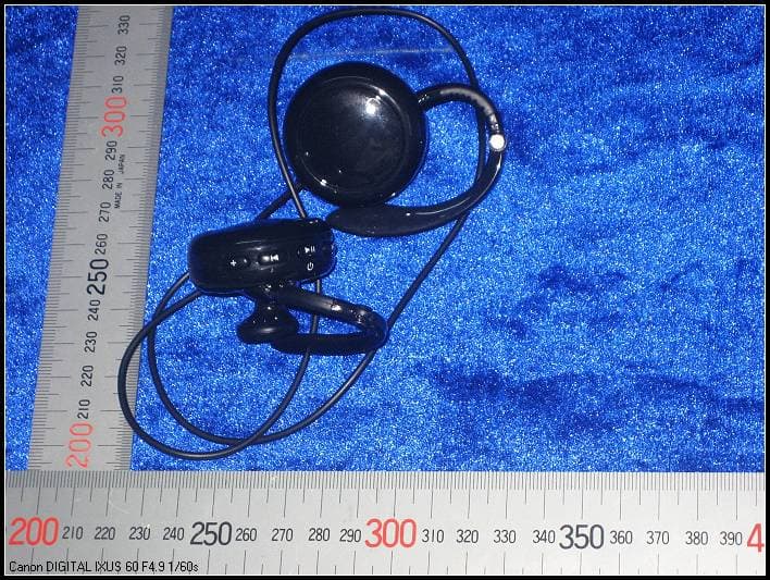
Click to zoom
Application Details
- Equipment Class
- DSS - Part 15 Spread Spectrum Transmitter
- Date of Grant
- Mar 09, 2008
- Application Purpose
- Original Equipment
- Date of Application
- Mar 09, 2008
- Equipment Note
- Bluetooth Headset
- Frequency Range
- 2402.00000000 - 2480.00000000
- Company
- FUNG SHING CO. LTD
- Country
- Hong Kong
Documents & Files
Document Text
Text extracted from the exhibit documents filed with the FCC. Open a document above to read the original.
Users Manual
FCC Statement This device complies with Part 15 of the FCC Rules. Operation is subject to the following two conditions: (1) this device may not cause harmful interference, and (2) this device must accept any interference received, including interference that may cause undesired operation. Changes or modifications not expressly approved by the party responsible for compliance could void the user's authority to operate the equipment. BT
Block Diagram
≤
ID Label/Location Info
FCC ID: VJ2FSCMYEAR-MBH1 This device complies with part 15 of the FCC rules. Operation is subject to the following two conditions (1) this device may not cause harmful interference, and (2) this device must accept any interference received, including interference that may cause undesired operation. Proposed Label Location on EUT FCC ID Label Location
Operational Description
The brief introduction of the circuit of the Bluetooth headsets 1. IC U1 crystal vibration Y1 16MHz will be launched out via antenna, after the 64 times frequency in U1, enlarged by the inside U1, exported passing TX_A and TX_A, and then going through the internet composed by T1、L1、L2、 C2、C14、C15 and filtered noises. 2. the adjusted signal adds via U1,XTAL_IN, by adjusting the change of frequency of Y1,16MHz, in order to reach the purpose which is to add the signal to the main frequency. 3. Lunching antenna is printing antenna, in fact, good effect can be obtained by PIFA antenna. 4. power of the whole body is provided by 3.7V battery. 5. Shooting frequency testing point, via a solid connecting frequency testing point on the designing connection board, puts a shooting frequency change connecting equipment on the sieve and antenna. 6. the memorizer of U2,FLASH uses the power provided by 1.8V, and the circuit can be changed easily. 1. FHSS characteristics The Bluetooth AFH construction (see Fig. 3). Add a group mapping in frequency synchromesh and frequency-hopping sequence generator. This mapping is a self- adjusting frequency selector in fact. Group mapping construction (see Fig. 4). Select a channel from the groups need to be divided, through PN mapping instrument, select channel mapping to grouping sequence from original frequency-hopping sequence. Enumerates grouping channel content in every channel list according to rising forward sequence. RF input signal Grouping Grouping sequence Figure 3 Bluetooth AFH Constructions N j Bad Bad Good From grouping serials and present serial is N j Figure 4 Group mapping construction Frequency synchromesh Group mapping Frequency-hopping sequence generator Grouping Group mapping Mod N j Select original frequency-hopping Sequence (0-78) Shift signal After grouping mapping, average shift signal balanced the channel usage. These shift signal is series counter, every counter indicate a group. The number J group is counting periodically in {0,1,2,...,Nj-1}scope. Nj is the number J channel number in grouping. The selected grouping counter is counting the next data. And take the data as the shift signal output. Channel is dynamically separated to 2 kinds of channel in Bluetooth: good channel NG and bad channel NB=79-NG, define N min is the minimum required frequency number required for Bluetooth communication equipment. Suitable for N min smaller than NG situation. All the frequency spot can be selected in good channel in this situation, as indicated in Fig. 5. When the frequency-hopping generator happens good channel, no new mapping will repeat. When the channel is bad in frequency-hopping sequence, then choose a better channel from a good channel storehouse. Through these 2 mode, in Bluetooth frequency selector, if the output channel is good, the use it directly; if it is the bad channel, then select frequency in good channel grouping. This selection avoids hit between the output frequency and other disturbing frequency. 3. Equal Hopping Frequency Use The EUT Complies with the Bluetooth RF specifications, for details refer to Bluetooth standards 4. Receiver input Bandwidth The receiver bandwidth is equal to to the receiver bandwidth in the 79 hopping channel mode, which is 1MHz, The receiver bandwidth was verified during Bluetooth RF conformance testing. 5. Receiver Hopping Capability The EUT Complies with the Bluetooth RF specifications, for details refer to Bluetooth standards
Schematics
1 2 3 4 5 6 78 ABCD 8 7 6 5 4 3 2 1 D CBA Title BC3MM External 7X7 Module Revision 0.07 Date 3-Jun-2005 VSS_PIO A1 VDD_PIO A2 PIO[11] A3 REB A4 D[1] A5 D[9] A6 D[3] A7 D[12] A8 D[6] A9 D[15] A10 A[16] A11 VSS_PADS A12 VDD_MEM A13 TXEN PIO[1] B1 PIO[3] B2 PIO[10] B3 CSB B4 D[8] B5 D[2] B6 D[10] B7 D[4] B8 D[13] B9 D[7] B10 TEST_EN B11 RESET B12 SPI_MISO B13 TXEN PIO[0] C1 PIO[2] C2 PIO[9] C3 A[0] C4 D[0] C5 VSS_CORE C6 VDD_CORE C7 D[11] C8 D[5] C9 D[14] C10 SPI_CSB C11 NC C12 SPI_CLK C13 VDD_RADIO D1 AUX_DAC D2 PIO[8] D3 VDD_PADS D11 SPI_MOSI D12 NC D13 RF_IN E1 VSS_RADIO E2 VSS_RADIO E3 VSS_CORE E11 RESETB E12 VDD_CORE E13 TX_B F1 VSS_RADIO F2 VSS F3 PIO[5] F11 PIO[4] F12 PIO[6] F13 TX_A G1 VSS_RADIO G2 VSS_RADIO G3 PIO[7] G11 NC G12 PCM_OUT G13 VSS_RADIO H1 VDD_RADIO H2 VSS_ANA H3 PCM_SYNC H11 NC H12 PCM_CLK H13 VSS_LO J1 VDD_LO J2 MIC_LEFT_P J3 PCM_IN J11 UART_TX J12 VSS_PADS J13 VSS_ANA K1 VDD_ANA K2 MIC_LEFT_N K3 UART_RX K11 UART_CTS K12 USB_DN K13 SPKR_LEFT_N L1 SPKR_RIGHT_N L2 MIC_RIGHT_P L3 AIO[1] L4 A[3] L5 VSS_ANA L6 A[6] L7 VDD_CORE L8 WEB L9 A[10] L10 A[13] L11 UART_RTS L12 USB_DP L13 SPKR_LEFT_P M1 SPKR_RIGHT_P M2 MIC_RIGHT_N M3 AIO[2] M4 A[2] M5 A[4] M6 A[5] M7 A[17] M8 VSS_CORE M9 A[9] M10 A[12] M11 A[15] M12 VDD_USB M13 XTAL_IN N1 XTAL_OUT N2 AIO[0] N3 AIO[3] N4 A[1] N5 VDD_ANA N6 VREG_IN N7 A[7] N8 A[18] N9 A[8] N10 A[11] N11 A[14] N12 VDD_MEM N13 U1BC352239A External 7X7 R51M R410K R647K R747K Y1 Toyocom TN-25888 16M C910P C83P3 C3 100n C4 15P R1047K R847K P1TE C6 10n C5 100n R1447K R1247K R1647K R1147K R947K R1547K R1347K R1747K R26 2.2R C174.7uF L1 2.2nH C22P L2 15nH C14 15P C15 15P REB G1 D[1] H2 D[9] G2 D[3] H3 D[12] F4 D[6] H5 DQ15/A-1 G6 A[16] E6 CSB F1 D[8] F2 D[2] E3 D[10] F3 D[4] H4 D[13] G5 D[7] E5 A[0] E1 D[0] E2 D[11] G3 D[5] E4 D[14] F5 A[3] A1 A[6] C2 WEB A4 A[10] C5 A[13] A6 A[2] C1 A[4] B1 A[5] D2 A[17] B2 A[9] A5 A[12] B6 A[15] D6 A[1] D1 A[7] A2 A[18] C3 A[8] B5 A[11] D5 A[14] C6 NC B3 NC D4 NC C4 NC D3 VCC G4 BYTEB F6 RESETB B4 VSS H6 VSS H1 RY/BYB A3 U8 MBM29SL800TE/BE C16 47n C7 4.7uF VMEM VMEM Unbalanced 1 GND 5 Balanced 4 Balanced 6 GND 7 DC 2 GND 8 NC 3 T1 DBF81F101 TP391.8/3.3V TP13.3V TP4 PIO0 TP5 PIO1 TP7 SPI_CLK TP8 SPI-MISO TP9 UART_RX TP10 UART_TX TP11PIO5 TP12PIO7 TP13PIO6 TP14PIO8 TP15RESET TP16GNDTP17GND TP19 SPI-CSB TP20 SPIO_MOSI TP21 UART_CTS TP22 UART_RTS TP24PIO3 TP25AIO0 TP26PIO4 TP27PIO9 TP29 SPKR_LEFT_N TP30 SPKR_RIGHT_P TP31 MIC_LEFT_P TP32 SPKR_RIGHT_N TP33 SPKR_LEFT_P TP34 MIC_LEFT_N TP35 PIO10 TP36 PIO11 TP37 MIC_RIGHT_N TP38 MIC_RIGHT_P C18 10n C19 4.7uF TP41RF-IN TP42 VDD-PA TP39 1.8V TP1 3.3V TP4 PIO0 TP5 PIO1 TP7 SPI_CLK TP8 SPI-MISO TP9 UART_RX TP10 UART_TX TP11 PIO5 TP12 PIO7 TP13 PIO6 TP14 PIO8TP15 RESET TP17 GNDTP47 GNDTP19 SPI-CSB TP20 SPIO_MOSI TP21 UART_CTS TP22 UART_RTS TP24 PIO3 TP25 AIO0 TP26 PIO4 TP27 PIO9 TP29 SPKR_LEFT_N TP30 SPKR_RIGHT_P TP31 MIC_LEFT_P TP32 SPKR_RIGHT_N TP33 SPKR_LEFT_P TP34 MIC_LEFT_N TP35 PIO10 TP36 PIO11 TP37 MIC_RIGHT_N TP38 MIC_RIGHT_P TP41 RF-INTP42 VDD-PA TP18 RF/OUT TP16 GND TP40 GND TP40 GND TP47GND TP18RF/OUT
Schematics
5 5 4 4 3 3 2 2 1 1 DD CC BB AA TMODE2 XIN XOUT 18VD 33VD33VD 33VD 18VD18VD18VD GND_D 18VD GND_D F_RE U_DM KEY_MENU C_CSB F_ALE F_CE1 C_SDA F_WE LCD_CS PWR_ON PLY_KEY U_DP F_CLE F_CE0 CHIP_RST C_SCL USB_DETF_WP F_IO1 F_IO2 F_IO7 F_IO0 F_IO5 F_RB F_IO4 F_IO6 F_IO3 SD_DT1 SD_DT3 SD_CMD SD_DT0 SD_DT2 SD_CLK AD_DATAAU_MCLKDA_CLRCAU_BCLKDA_DATA REC LCD_D4 LCD_D1 LCD_D3 LCD_D2 LCD_D6 LCD_A0 LCD_D7 LCD_D5 LCD_D0 LCD_W/RLED_ONKEY_MENU V+ NEXT PREVV-EQ BAT_CHK SD_DET LCD_RD KEY_CE MP3_CE CH_HK Title SizeDocument NumberRev Date:Sheetof <Doc><RevCode> <Title> A4 15Thursday, November 22, 2007 Title SizeDocument NumberRev Date:Sheetof <Doc><RevCode> <Title> A4 15Thursday, November 22, 2007 Title SizeDocument NumberRev Date:Sheetof <Doc><RevCode> <Title> A4 15Thursday, November 22, 2007 C B A Y0 Y1 Y2 Y3 Y4 Y5 Y6 NEXT PREV EQ REC FNU REPEAT STOP I/O REC “H” line in “L” KEY_CE ”L” ”L“ ”H“ U2 NX5850 U2 NX5850 TMOD0 1 TMOD1 2 TMOD2 3 TMOD3 4 TMOD4 5 33VD1 6 33GD1 7 U_DP 8 U_DM 9 ADDR3 10 ADDR2 11 ADDR1 12 ADDR0 13 P00 14 P01 15 P02 16 33VD2 17 33GD2 18 P03 19 P04 20 P05 21 P06 22 P07 23 P22 24 M_PSEN 25 18VD1 26 18GD1 27 P_10 28 P_11 29 P_12 30 P_13 31 P_14 32 P_15 33 P_16 34 P_17 35 33GD3 36 33VD3 37 P30/RXD 38 P31/TXD 39 P32/INT0 40 P33/INT1 41 P34/T0 42 P35/T1 43 P36/WR 44 P37/RD 45 M_ALE 46 18GD2 47 18VD2 48 KEY_0 49 KEY_1 50 KEY_2 51 KEY_3 52 KEY_4 53 KEY_5 54 KEY_6 55 KEY_7 56 33GD4 57 33VD4 58 SDOUT 59 SDIN 60 CCLK 61 SCLK 62 MCLK 63 M_CLK 64 DATA 65 M_CMD 66 18GD3 67 18VD3 68 P_23 69 P_21 70 P_20 71 P_25 72 P_26 73 GPIO0 74 GPIO1 75 GPIO2 76 GPIO3 77 GPIO4 78 GPIO5 79 33GD5 80 33VD5 81 P_27 82 P_24 83 ADR7 84 ADR6 85 ADR5 86 ADR4 87 F_R/B 88 F_IO7 89 F_IO6 90 F_IO5 91 F_IO4 92 F_IO3 93 F_IO2 94 F_IO1 95 F_IO0 96 F_CE3 97 F_CE2 98 F_CE1 99 F_CE0 100 18VD4 101 18GD4 102 F_CLE 103 F_ALE 104 F_WEN 105 F_REN 106 33VD6 107 33GD6 108 X_IN 109 XOUT 110 18DV1 111 18DG1 112 FILTER 113 18AG1 114 18AV1 115 33AG2 116 33AV2 117 A_IN3 118 A_IN2 119 A_IN1 120 A_IN0 121 AGD3 122 VREF 123 33DG2 124 33DV2 125 NRST 126 XRM 127 LCD 128 C6 104 C6 104 C23 104 C23 104 C13 104 C13 104 R2300KR2300K C10 104 C10 104 C7 104 C7 104 C16 105 C16 105 C11 104 C11 104 C15 22P C15 22P C2 104 C2 104 U181C29L-Q-3U181C29L-Q-3 23 1 C5 104 C5 104 R11MR11M X112MHzX112MHz 12 C32 104 C32 104 C21 104 C21 104 C1 104 C1 104 C12 104 C12 104 C9 104 C9 104 C4 104 C4 104 C3 104 C3 104 C14 22P C14 22P C8 104 C8 104 5 5 4 4 3 3 2 2 1 1 DD CC BB AA GND BAT+ GND GNDGND GND MICBAS MICBAS GND BAT+ GND GND 1V8 GND GND GND GND GND B_BAT+ GND_P GND 1V8 BAT+ GND_PGND GND GND GND BAT+ GND GND B_BAT+ GND MICR- MICL- MICL+ GP10 V+ GP9 B_PP MIC_IN GP4 GP4 NEXT PREV GP10 MICR- MICL- MICL+ MICR+ MICR- MICL- MICL+ MICR+ GP9 RESET BR- GP9 BR+ MIC+ BL+ BL- SPL+ SPR- SPR+ SPL+ SPL- ON/OFF MIC- SPL- GP9 BLUE_LED RED_LED V- MICR+ GP6 BLUE_LED RED_LED REC SPR- SPR+ Title SizeDocument NumberRev Date:Sheetof <Doc><RevCode> <Title> A4 11Friday, December 21, 2007 Title SizeDocument NumberRev Date:Sheetof <Doc><RevCode> <Title> A4 11Friday, December 21, 2007 Title SizeDocument NumberRev Date:Sheetof <Doc><RevCode> <Title> A4 11Friday, December 21, 2007 GPIO GPIO0 V- GPIO1 V+ GPIO2 PLAY/PAUSE GPIO8 GPIO10 C38 104 C38 104 R660RR660R R75 47K R75 47K R63 1M R63 1M + E4 22uF/6V/P + E4 22uF/6V/P + E1 10uF/6V/P + E1 10uF/6V/P Q3AP2305Q3AP2305 R56 100K R56 100K R59 150K R59 150K R39 4.7K R39 4.7K L10 B100 L10 B100 C112 104 C112 104 Q12 KTC4075E(NPN) Q12 KTC4075E(NPN) R73 47K R73 47K R5347KR5347K R00 0R R00 0R C55 104 C55 104 C41 22pF C41 22pF C113 104 C113 104 LED1 LED LED1 LED 1 2 3 4 L6 B100 L6 B100 C45473C45473 R52 47K R52 47K R42 100K R42 100K ANT2 FPC_ANT ANT2 FPC_ANT 12 U4 XC6219B302MR U4 XC6219B302MR IN 1 G 2 EN 3 BP 4 OUT 5 U11 RT8008 U11 RT8008 IN 1 G 2 CE 3 OUT 4 LX 5 + E2 22uF/6V/P + E2 22uF/6V/P R690RR690R R3047KR3047K Q4 KTC4075E(NPN) Q4 KTC4075E(NPN) C42473C42473 U13 BLUETHOOTH U13 BLUETHOOTH SPR- 1 SPR+ 2 GND 3 MICR+ 4 MICR- 5 MICL- 6 MICL+ 7 GND 8 1.8V 9 P_9 10 A_1 11 A_2 12 A_3 13 3.3Vout 14 GND 15 3.7Vin 16 U_RTS 17 U_CTS 18 U_TX 19 U_RX 20 P_7 21 P_6 22 P_4 23 GND 24 P_CLK 25 P_OUT 26 P_SYNC 27 P_IN 28 P_5 29 RST 30 SPI_MISO 31 SPI_CLK 32 SPI_MISI 33 SPI_CSB 34 P_11 35 P_10 36 P_8 37 P_3 38 P_2 39 P_1 40 P_0 41 GND 42 ANT 43 GND 44 SPL- 45 SPL+ 46 R60 150K R60 150K C43473C43473 R88 NC R88 NC R61 100K R61 100K R402.2KR402.2K C44473C44473 Q15 KTC4075E(NPN) Q15 KTC4075E(NPN) C54 104 C54 104 L14 22uH L14 22uH C46 1uF C46 1uF R55 330R R55 330R R62 1M R62 1M R54 330R R54 330R D11SS355TE-17D11SS355TE-17 R6447KR6447K 5 5 4 4 3 3 2 2 1 1 DD CC BB AA KEY_C RST BAT+ BAT+ 33VD GNDGND 33VD 33VD 3.3Vout GND GND GND GND 3.3Vout PLAY PREV NEXT EQ V- KEY_MENU V+ PLAYB_PP ON/OFF LCD_D0 LCD_D1 LCD_A0 LCD_D5 LCD_W/R LCD_CS LCD_D6 CHIP_RST LCD_D7 LCD_D2 LCD_D4 LCD_D3 LCD_RD LED_ON V+ PREV NEXT EQ V- KEY_MENU V+ PREV CHIP_RST NEXT RESET KEY_CE GP6 REC GP6_CE GP6 Title SizeDocument NumberRev Date:Sheetof <Doc><RevCode> <Title> A4 11Monday, December 10, 2007 Title SizeDocument NumberRev Date:Sheetof <Doc><RevCode> <Title> A4 11Monday, December 10, 2007 Title SizeDocument NumberRev Date:Sheetof <Doc><RevCode> <Title> A4 11Monday, December 10, 2007 RESET [V+] + [PREV] = MP3 RESET [V+] + [NEXT] = Bluetooth RESET Q14 KTC4075E(NPN) Q14 KTC4075E(NPN) C69 104 C69 104 R37 22K R37 22K R82 5.6K R82 5.6K Q17 KTC4075E(NPN) Q17 KTC4075E(NPN) SW91100ESW91100E D8 1SS355TE-17 D8 1SS355TE-17 B+2 LED+ B+2 LED+ 1 R78 22K R78 22K R9547KR9547K SW141100ESW141100E R90 47K R90 47K R26 5.6K R26 5.6K R96 NC R96 NC SW151100ESW151100E R94 5.6K R94 5.6K LCD1 MTC1002 64X48 LCD1 MTC1002 64X48 VDD 1 V86 2 VSS 3 V0 4 V1 5 V2 6 V3 7 V4 8 C2N 9 C2P 10 C1P 11 C1N 12 C3P 13 Vout 14 Vss 15 D7 16 D6 17 D5 18 D4 19 D3 20 /RES 27 A0 26 WR/ 25 RD/ 24 D0 23 D1 22 D2 21 /CS 28 C64 104 C64 104 D7 1SS355TE-17 D7 1SS355TE-17 SW111100ESW111100E C66 104 C66 104 C62 104 C62 104 SW81185ESW81185E Q11 KTA2014E(PNP) Q11 KTA2014E(PNP) R91 0R R91 0R R28 5.6K R28 5.6K C68 104 C68 104 R97 5.6K R97 5.6K C70 104 C70 104 R29 5.6K R29 5.6K R79 10K…
Text truncated - open the document above for the full version.
Test Report
ISO/IEC17025Accredited Lab. Report No: FCC 0712230 File reference No: 2008-02-22 Applicant: FUNG SHING CO., LTD Product: Built-In MP3 + Bluetooth Headset Model No: MyEar-MBH Trademark: N/A Test Standards: FCC Part 15 Subpart C, Paragraph 15.247 Test result: It is herewith confirmed and found to comply with the requirements set up by ANSI C63.4&FCC Part 15 Subpart C, Paragraph 15.247 regulations for the evaluation of electromagnetic compatibility Approved By Jack Chung Manager Dated: Feb 22,2008 Results appearing herein relate only to the sample tested The technical reports is issued errors and omissions exempt and is subject to withdrawal at SHENZHEN TIMEWAY TECHNOLOGY CONSULTING CO LTD 5/F,Block 4, Anhua Industrial Zone.,No.8 TaiRan Rd.CheGongMiao,FuTian District, Shenzhen,CHINA. Tel (755) 83448688 Fax (755) 83442996 Report No: 0712230 Page 2 of 64 Date: 2008-02-22 TEST REPORT The report refers only to the sample tested and does not apply to the bulk. This report is issued in confidence to the client and it will be strictly treated as such by the Shenzhen Timeway Technology Consulting Co .,Ltd. It may not be reproduced rather in its entirety or in part and it may not be used for adverting. The client to whom the report is issued may, however, show or send it . or a certified copy there of prepared by the Shenzhen Timeway Technology Consulting co .,Ltd to his customer. Supplier or others persons directly concerned. Shenzhen Timeway Technology Consulting co .,Ltd will not, without the consent of the client enter into any discussion of correspondence with any third party concerning the contents of the report. In the event of the improper use of the report. The Shenzhen Timeway Technology Consulting co .,Ltd reserves the rights to withdraw it and to adopt any other remedies which may be appropriate. Special Statement: The testing quality ability of our laboratory meet with "Quality Law of People's Republic of China" Clause 19. The testing quality system of our laboratory meets with ISO/IEC-17025 requirements, which is approved by CNAS. This approval result is accepted by MRA of APLAC. Our test facility is recognized, certified, or accredited by the following organizations: CNAS-LAB Code: L2292 The EMC Laboratory has been assessed and in compliance with CNAS-CL01 accreditation criteria for testing Laboratories (identical to ISO/IEC 17025:1999 General Requirements) for the Competence of testing Laboratories. FCC-Registration No.: 899988 The EMC Laboratory has been registered and fully described in a report filed with the (FCC) Federal Communications commission. The acceptance letter from the FCC is maintained in our files. Registration No.:899988. IC- Registration No.: IC5205A-01 The EMC Laboratory has been registered and fully described in a report filed with the (IC) Industry Canada. The acceptance letter from the IC is maintained in our files. Registration No.: IC 5205A-01. Report No: 0712230 Page 3 of 64 Date: 2008-02-22 TEST REPORT The report refers only to the sample tested and does not apply to the bulk. This report is issued in confidence to the client and it will be strictly treated as such by the Shenzhen Timeway Technology Consulting Co .,Ltd. It may not be reproduced rather in its entirety or in part and it may not be used for adverting. The client to whom the report is issued may, however, show or send it . or a certified copy there of prepared by the Shenzhen Timeway Technology Consulting co .,Ltd to his customer. Supplier or others persons directly concerned. Shenzhen Timeway Technology Consulting co .,Ltd will not, without the consent of the client enter into any discussion of correspondence with any third party concerning the contents of the report. In the event of the improper use of the report. The Shenzhen Timeway Technology Consulting co .,Ltd reserves the rights to withdraw it and to adopt any other remedies which may be appropriate. Test Report Conclusion Content 1.0 General Details ................................................................................................ 3 1.1 Test Lab Details................................................................................................ 3 1.2 Applicant Details.............................................................................................. 3 1.3 Description of EUT .......................................................................................... 3 1.4 Submitted Sample............................................................................................. 3 1.5 Test Duration.................................................................................................... 4 1.6 Test Uncertainty.................................................................................................4 1.7 Test By.......................................................................................................... 4 2.0 List of Measurement Equipment......................................................................... 4 3.0 Technical Details............................................................................................. 7 3.1 Summary of Test Results..................................................................................... 7 3.2 Test Standards.................................................................................................. 7 4.0 EUT Modification............................................................................................. 7 5.0 Power Line Conducted Emission Test...................................................................... 8 5.1 Schematics of the Test........................................................................................ 8 5.2 Test Method and Test Procedure............................................................................ 8 5.3 Configuration of the EUT.................................................................................... 8 5.4 EUT Operating Condition........................................…
Text truncated - open the document above for the full version.
Test Report
Report No: 0712230 Page 33 of 64 Date: 2008-02-22 TEST REPORT The report refers only to the sample tested and does not apply to the bulk. This report is issued in confidence to the client and it will be strictly treated as such by the Shenzhen Timeway Technology Consulting Co .,Ltd. It may not be reproduced rather in its entirety or in part and it may not be used for adverting. The client to whom the report is issued may, however, show or send it . or a certified copy there of prepared by the Shenzhen Timeway Technology Consulting co .,Ltd to his customer. Supplier or others persons directly concerned. Shenzhen Timeway Technology Consulting co .,Ltd will not, without the consent of the client enter into any discussion of correspondence with any third party concerning the contents of the report. In the event of the improper use of the report. The Shenzhen Timeway Technology Consulting co .,Ltd reserves the rights to withdraw it and to adopt any other remedies which may be appropriate. 3. High Channel Report No: 0712230 Page 34 of 64 Date: 2008-02-22 TEST REPORT The report refers only to the sample tested and does not apply to the bulk. This report is issued in confidence to the client and it will be strictly treated as such by the Shenzhen Timeway Technology Consulting Co .,Ltd. It may not be reproduced rather in its entirety or in part and it may not be used for adverting. The client to whom the report is issued may, however, show or send it . or a certified copy there of prepared by the Shenzhen Timeway Technology Consulting co .,Ltd to his customer. Supplier or others persons directly concerned. Shenzhen Timeway Technology Consulting co .,Ltd will not, without the consent of the client enter into any discussion of correspondence with any third party concerning the contents of the report. In the event of the improper use of the report. The Shenzhen Timeway Technology Consulting co .,Ltd reserves the rights to withdraw it and to adopt any other remedies which may be appropriate. 8. Maximum Peak Output Power 8.1 Regulation According to §15.247(b)(1), for frequency hopping systems operating in the 2400-2483.5 MHz band employing at least 75 non-overlapping hopping channels, and all frequency hopping systems in the 5725-5850 MHz band: 1 watt. For all other frequency hopping systems in the 2400-2483.5MHz band:0.125 watts. According to §15.247(b)(4), the conducted output power limit specified in paragraph (b) of this section is based on the use of antennas with directional gains that do not exceed 6 dBi. Except as shown in paragraph (c) of this section, if transmitting antennas of directional gain greater than 6 dBi are used, the conducted output power from the intentional radiator shall be reduced below the stated values in paragraphs (b)(1), (b)(2), and (b)(3) of this section, as appropriate, by the amount in dB that the directional gain of the antenna exceeds 6 dBi. 8.2 Limits of Maximum Peak Output Power The Maximum Peak Output Power Measurement is 30dBm. 8.3 Test Procedure 1. Check the calibration of the measuring instrument (spectrum analyzer) using either an internal calibrator or a known signal from an external generator. 2. Set the spectrum analyzer as follows: Span = approximately 5 times the 20 dB bandwidth, centered on a hopping channel; RBW > the 20 dB bandwidth of the emission being measured; VBW ≥ RBW; Sweep = auto; Detector function = peak; Trace = max hold 3. Measure the highest amplitude appearing on spectral display and record the level to calculate results. 4. Repeat above procedures until all frequencies measured were complete. Report No: 0712230 Page 35 of 64 Date: 2008-02-22 TEST REPORT The report refers only to the sample tested and does not apply to the bulk. This report is issued in confidence to the client and it will be strictly treated as such by the Shenzhen Timeway Technology Consulting Co .,Ltd. It may not be reproduced rather in its entirety or in part and it may not be used for adverting. The client to whom the report is issued may, however, show or send it . or a certified copy there of prepared by the Shenzhen Timeway Technology Consulting co .,Ltd to his customer. Supplier or others persons directly concerned. Shenzhen Timeway Technology Consulting co .,Ltd will not, without the consent of the client enter into any discussion of correspondence with any third party concerning the contents of the report. In the event of the improper use of the report. The Shenzhen Timeway Technology Consulting co .,Ltd reserves the rights to withdraw it and to adopt any other remedies which may be appropriate. 8.4Test Results EUT Built-In MP3 + Bluetooth Headset Model MyEar-MBH Mode Keeping Transmitting Input Voltage DC5V Temperature 24 deg. C, Humidity 56% RH Channel Channel Frequency (MHz) Peak Power Output (dBm) Peak Power Limit (dBm) Pass/ Fail Low 2402 -11.37 30 Pass Middle 2441 -11.60 30 Pass High 2480 -10.64 30 Pass Note: 1. the result basic equation calculation as follow: Peak Power Output = Peak Power Reading + Cable loss + Attenuator Report No: 0712230 Page 36 of 64 Date: 2008-02-22 TEST REPORT The report refers only to the sample tested and does not apply to the bulk. This report is issued in confidence to the client and it will be strictly treated as such by the Shenzhen Timeway Technology Consulting Co .,Ltd. It may not be reproduced rather in its entirety or in part and it may not be used for adverting. The client to whom the report is issued may, however, show or send it . or a certified copy there of prepared by the Shenzhen Timeway Technology Consulting co .,Ltd to his customer. Supplier or others persons directly concerned. Shenzhen Timeway Technology Consulting co .,Ltd will not, without the consent of the client enter into any discussion of correspondence with any third party concerning the contents of the report. In the event of the improper use of the report. The Shenzhen Timeway Technology Consulting co .,Ltd reserves the rights to withdraw it and to ad…
Text truncated - open the document above for the full version.
Contact Information
Applicant
Kennis Lee(Manager)
Test Firm
Shenzhen Timeway Testing LaboratoriesJack Chung
Technical Specifications
| # | Rule Parts | Frequency Range | Power Output |
|---|---|---|---|
| 1 | 15C | 2.40 GHz - 2.48 GHz | 100.00 µW |
Other Applications from FUNG SHING CO. LTD
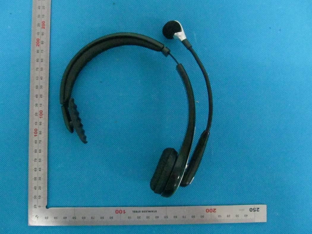
VJ2THEBOOM-W
May 30, 2013Bluetooth Headset
Equipment Class
DSS - Part 15 Spread Spectrum Transmitter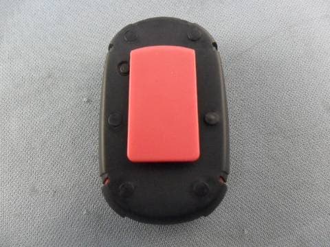
VJ2FSSG04
Aug 28, 2011Waterproof MP3 Player
Equipment Class
JBP - Part 15 Class B Computing Device Peripheral
VJ2FSFM002TR
May 02, 201049MHZ Wireless earphone
Equipment Class
DXX - Part 15 Low Power Communication Device Transmitter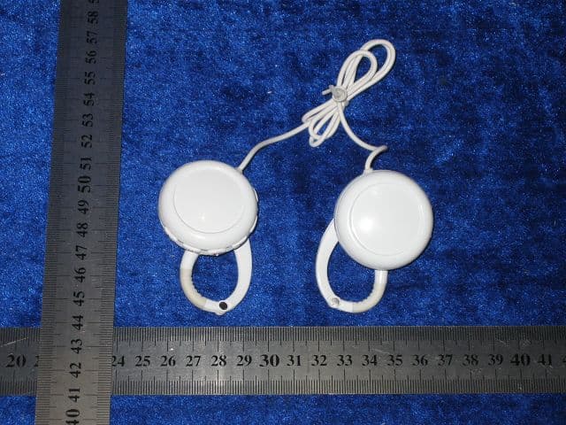
VJ2FSCMYEAR-BTH1
Oct 25, 2007Bluetooth Stereo Headset
Equipment Class
DSS - Part 15 Spread Spectrum Transmitter