WA6I601GSM/GPRS Dual-band Mobile Phone
VeryKool USA Inc
Click to zoom
Application Details
- Equipment Class
- PCE - PCS Licensed Transmitter held to ear
- Date of Grant
- Dec 20, 2012
- Application Purpose
- Original Equipment
- Date of Application
- Dec 20, 2012
- Equipment Note
- GSM/GPRS Dual-band Mobile Phone
- Frequency Range
- 1850.20000000 - 1909.80000000
- Company
- VeryKool USA Inc
- Country
- United States
Documents & Files
Document Text
Text extracted from the exhibit documents filed with the FCC. Open a document above to read the original.
Users Manual
User Guide Welcome to use your new product. Registering your new cell phone will take you less than 2 minutes and will give you access to the verykool zone where you will enjoy from promotions, ringtones, technical information, support and much more. Visit: www.verykoolzone.com Functions Description 1.Left soft key (LSK) 7.Keypad 2.Right soft key (RSK) 8.Receiver 3.Send key (Snd) 9.USB jack 4.End key (End) 10.Camera 5.Navigation key 11.Speaker 6.OK key 12.Flashlight/Torch Welcome to use i601 Make a call In the standby mode Input the number Press Snd key to call End a call Press End key Add a new contact Enter Phonebook Options Choose New OK Select To SIM/ Phone Choose the field to Edit When finished editing fields, select Save to save Send a msg Message Write message Edit message content Once done typing press OK key Enter recipient or add from phonebook Press OK key Send WAP WAP Options Choose Open Choose Go to URL Input address Press OK key to browse Audio player Entertainment Audio player Press LSK Choose Music list With my i601 I want to... Select one list Press OK key Options Choose Add music Add music from memory card Press OK key to play FM Radio FM Radio Press Down Key to activate or deactivate Press Left/Right Key to adjust the radio frequency. Press -/+ Key to adjust the player volume Take a picture Entertainment Camera Press OK key to take pictures Bluetooth Extras Bluetooth Open/Close Bluetooth Select to switch on/off Bluetooth Accessories in Package Handset Battery Travel charger Earphone User Guide 1 pcs 1 pcs 1 pcs 1 pcs 1 pcs Security and performance ◆Do not touch the screen of the mobile phone with sharp objects. Dust particles and nails may scratch the screen. Please maintain the screen clean. Please gently remove the dust on the screen with soft cloth to avoid any damages to the screen. ◆In thunder raining days, please do not use the mobile phone when charging it or outdoor, so as to avoid being struck by thunder or other injuries. ◆Please do not put the battery in high-temperature environment (high temperature will lead to heat of the battery upgrading), or else it may result in fire or explosion. ◆Please keep the mobile phone charged and keep charger away from people or other flammable and explosive articles in order to avoid fire, explosion or other dangers! ◆Please follow the rules strictly and shut down the mobile phone on occasions when use of mobile phone is prohibited! ◆Please do not put the mobile phone, battery and charger in the equipment with strong electromagnetic field, such as induction cooker and microwave oven; otherwise it will lead to circuit failure, fire or explosion. ◆Please do not arbitrarily refit the mobile phone, or teardown the mobile phone and accessories without authorization. Improper refitting or teardown may trigger fire and explosion of the mobile phone. Only the authorized service centers can repair the mobile phone. ◆Please do not use battery, charger or accessories of non-standard original models. ◆Please do not join the two poles of the battery, so as not to result in battery short-circuit. ◆Please do not use the mobile phone if the power wire has been damaged (such as the exposed and fractured), or the connector has been loosened, so as to avoid electric shock, short circuit of the charger or fire. ◆The mobile phone should be powered off in the hospital or other places where use of mobile phone is prohibited. Mobile phone will affect proper functionality of electronic equipment and medical devices, such as pacemakers, hearing aids and other medical electronic equipment. Pacemaker manufacturer proposes to keep the distance between the mobile phone and the pacemaker at least 15 cm (no comma) in order to avoid potential interference by the mobile phone. ◆Please do not use the mobile phone when driving a car. In case of emergency, please use hand-free devices (which may be bought separately); otherwise, please park your car on the road side before making a call. ◆Please do not put the mobile phone on car insurance airbag or region reachable by the airbag after spreading. Otherwise when the airbag expands or ruptures, the mobile phone is likely to cause serious damage to the people in the car due to strong external force. ◆Please keep the mobile phone, battery and charger at place out of the reach of children. Please do not let children use the mobile phone, battery and charger in the absence of adults’ supervision. ◆In order to comply with provisions of RF leakage, when you wear a mobile phone or use the data functions of the mobile phone, please maintain the distance between the antenna and the body at least 1 inch (2.5 centimeters). ◆Please power off the mobile phone before cleaning and maintenance. If the mobile phone is connected to the charger, you need to unplug the charger from the power outlet, and disconnect the connection between the charger and the mobile phone in order to avoid electric shock, short circuit of battery or charger. ◆Do not use chemical lotion, scrubbing cleanser to wipe the mobile phone or the charger, otherwise it may damage the components or cause fire. Slightly wet and anti-static soft clean cloth can be used. ◆Please do not throw used lithium batteries into trash can, send them to the designated recycling center or return them to our company. ◆Please do not charge the mobile phone in dusty or humid environment or extreme temperature (the permitted charging temperature range is 0°C~ 40°C), and the power wire cannot be nearby the heating containers. ◆In the use of network function, if the users download a file with virus, which make the mobile phone cannot be used normally; the company does not undertake any responsibility arising therefore. Warning: The original manufacturer will not take on any responsibility for the users who are not in compliance with the above advices or improperly use the mobile phone. Note: The application of value-added services of the mobile phone is provided by relevant service pr…
Text truncated - open the document above for the full version.
External Photos
Verykool USA Inc Model: I601 REPORT NO.: STR12128052I-1 FCC PART 22H & 24E EXHIBIT 2 - EUT EXTERNAL PHOTOGRAPHS EUT View EUT View_Front Verykool USA Inc Model: I601 REPORT NO.: STR12128052I-1 FCC PART 22H & 24E EUT View_Rear EUT View_Up Verykool USA Inc Model: I601 REPORT NO.: STR12128052I-1 FCC PART 22H & 24E EUT View_Down EUT View_Left Side Verykool USA Inc Model: I601 REPORT NO.: STR12128052I-1 FCC PART 22H & 24E EUT View_Right Side
ID Label/Location Info
Verykool USA Inc Model: I601 REPORT NO.: STR12128052I-1 FCC PART 22H & 24E EXHIBIT 1- PRODUCT LABELING Proposed FCC ID Label Format FCC ID: WA6I601 Specifications : Text is Black in color and justified. Labels are printed in indelible ink on permanent adhesive silk-screened onto the EUT or shall be affixed at a conspicuous location on the EUT. Proposed Label Location on EUT FCC ID Label Location
Internal Photos
Verykool USA Inc Model: I601 REPORT NO.: STR12128052I-1 FCC PART 22H & 24E EXHIBIT 3 - EUT INTERNAL PHOTOGRAPHS EUT Housing and Board View 1 EUT Housing and Board View 2 GSM Antenna Verykool USA Inc Model: I601 REPORT NO.: STR12128052I-1 FCC PART 22H & 24E Solder Board-Component View 1 Solder Board-Component View 2 Bluetooth Antenna Verykool USA Inc Model: I601 REPORT NO.: STR12128052I-1 FCC PART 22H & 24E Solder Board-Component View 3 Solder Board-Component View 4
Operational Description
Circuit Description 1 RF circuit 1.1 Main functions of RF circuit: The baseband modulate the uplink signal, and then transmit it on RF carrier by the antenna; Demodulate the received wireless signal transmitted by the base station by the receiving circuit then get the forward signal; at the same time, provide the steady en-control 26MHz frequency source. 1.2 Structure of RF circuit: We can divide it to 4 units according to the functions: Antenna unit, frequency synthesized unit, receiving unit, transmitting unit. 1.2.1 Antenna unit Antenna unit is composed by antenna groupware, antenna switch and RF7168. This antenna groupware is the transceiver of the wireless signal that is composed by inside antenna, and could fetch up the disadvantages such as the low efficiency and the poor radiance direction by the high performance match. 1.2.2 Frequency-synthesized unit The SR528 has a single fast-locking fractional synthesizer used for VCO control in both receive and transmit mode. The entire system including VCO, tank, fractional N dividers, sigma delta compensation, charge pump and loop filters are fully integrated. The only external component is the frequency reference. The synthesizer is controlled via the serial interface. The VCO is fed into the respective dividers to generate the appropriate LO frequencies for the RX and TX bands. Fractional N Dividers The fractional N divider allows the PLL system to have a smaller step size than the comparison frequency which is set by the external reference to 26 MHz. This feature allows all the GSM frequency band raster to be achieved, with fast lock times and good phase noise characteristics. The divider section consists of a dual modulus 8/9 prescaler, integer M & A dividers, and fractional N system based on sigma-delta modulation to generate the required fractional divide ratio. The Denominator of the fractional divider can be set to 3 different values, (1040, 1170, 1235), depending on the mode of operation. For example a denominator of 1040 with an input fraction F maintains an average value of F/1040 allowing 25 kHz steps when operated at a reference of 26 MHz. Phase Frequency Detector/Charge Pump A Phase Frequency Detector (PFD) is used for the PLL phase detector. The charge pump is designed such that good matching of up and down currents is achieved over a wide output operating range. The charge pump output is internally routed to the integrated synthesizer loop filter. Synthesizer Loop filter To minimize complexity of the external PCB layout the Main Synthesizer loop filter is also fully integrated into the IC. No external components or adjustments are required. Voltage Controlled Oscillator The integrated voltage controlled oscillator (VCO) is a complete self- calibrating subsystem. This employs a fully auto-mated digital self- calibration function to ensure optimum phase noise performance over the entire frequency range. The VCO generates frequencies between 2520MHz and 2985MHz as required to operate in the four GSM bands for RX and TX. Reference Oscillator The SR528 requires only an external low cost crystal as the frequency reference. The circuitry to oscillate the crystal and tune its frequency is fully integrated. For good noise immunity the oscillator is a balanced implementation requiring the crystal to be connected across 2 pins. There is a programmable capacitor array included for coarse tuning of fixed offsets (e.g. crystal manufacturing tolerance), and an integrated varactor for dynamic control. The oscillator is designed for use with a 26MHz crystal. 1.3. Transmitting unit The transmit section of the SR528 radio implements a translation loop modulator. This consists of a quadrature modulator, high speed phase- frequency detector (PFD) with charge pump output, loop filter, TX VCO and a feedback down converting mixer. The VCO output (divided by 2 for low band) is fed to the power amplifier with a portion internally fed back into the down-converting feedback mixer to close the feedback loop. The Quadrature modulator takes the baseband I & Q signals and translates these into a GMSK signal at the Transmit Inter-mediate Frequency (TX IF). After bandpass filtering and limiting the TX IF signal is used as the reference input to the Phase Frequency Detector (PFD) of the transmit PLL. Phase Frequency Detector (PFD) The PFD ensures that the transmitted signal contains the required modulation and is accurately locked to the desired GSM channel. The downconverted feedback signal from the TX VCO and the Quadrature Modulator output are phase compared by the PFD. The PFD charge pump generates a current pulse proportional to the difference in phase which is applied to the loop filter. Loop filter To minimize complexity of the external PCB layout the TX loop filter is fully integrated into the IC. At power up the filter is automatically calibrated as part of the baseband filter cal, eliminating process tolerances. The calibration is fully integrated and requires no extra programming. TX VCO The Transmit Voltage Controlled Oscillator (TX VCO) and tank components are a fully integrated subsystem. The subsystem includes PA drivers so the outputs are used to directly drive the external PAs. The low noise oscillator design and internal filtering mean that external TX SAW filters are not required. In Low band operation the TX VCO output is divided by two and filtered. The TX VCO is automatically calibrated to ensure optimum performance over its operating frequency of 1648 to 1910 MHz. Feedback Down-Converting Mixer The feedback down converting mixer is used to translate the TX VCO output frequency to the TX IF. An integrated band pass filter exists between the mixer and the PFD to filter the mixers unwanted side band and higher order mixing products. Transmit Frequency Plan Unlike many other translation loop modulators the SR528 uses only a single VCO source to derive the local oscillator signal for both the Feedback Down-Converting Mixer and the Quadratu…
Text truncated - open the document above for the full version.
Parts List/Tune Up Info
No.P/ACODEDescriptionUnitNUM.REF. 001PH-0502-000JB0-B00Resistance,0 ohm,±5%,1/16W,0402PCS13R301,R402,R403,R2,R901,R414,C450,B905,B906,R1206,R1207,R1301 ,C1319 002PH-0502-036FE0-D00Resistance,0.36 ohm,±1%,1/4W,0805PCS1R300 003PH-0502-100JB0-B00Resistance,10 ohm,±5%,1/16W,0402PCS6R303,R702,R703,R704,R705,R805 004PH-0502-330JB0-B00Resistance,33 ohm,±5%,1/16W,0402PCS12R103,R202-R203,R903-R904,R1001-R1007 005PH-0502-101JB0-B00Resistance,100 ohm,±5%,1/16W,0402PCS15R600,R604,R1302-R1312,R1315,R1316 006PH-0502-511JB0-B00Resistance,510 ohm,±5%,1/16W,0402PCS2R605-R606 007PH-0502-102JB0-B00Resistance,1K ohm,±5%,1/16W,0402PCS10R201,R601,R615,R941,R942,R1000,R1321-R1324 008PH-0502-152JB0-B00Resistance,1.5K ohm,±5%,1/16W,0402PCS2R608-R609 009PH-0502-202JB0-B00Resistance,2K ohm,±5%,1/16W,0402PCS5R614,R802-R804,R906 010PH-0502-512JB0-B00Resistance,5.1K ohm,±5%,1/16W,0402PCS1R1203 011PH-0502-622FB0-B00Resistance,6.2K ohm,±1%,1/16W,0402PCS1R200 012PH-0502-103JB0-B00Resistance,10K ohm,±5%,1/16W,0402PCS2R621,R622 013PH-0502-153JB0-B00Resistance,15K ohm,±5%,1/16W,0402PCS2R401,R623 014PH-0502-473JB0-B00Resistance,47K ohm,±5%,1/16W,0402PCS3R1115-R1116,R3 015PH-0502-753JB0-B00Resistance,75K ohm,±5%,1/16W,0402PCS1R624 016PH-0502-154JB0-B00Resistance,150K ohm,±5%,1/16W,0402PCS1R1330 017PH-0504-502050-B00ESD,Varistor,5.5V,0402,AVLC5S02050,AMOTECHPCS14VR600-VR605,VR701-VR705,VR905,VR906,VR1000 018AH-0504-100555-400ESD,Varistor,5.5V,0402,SDV1005E5R5C400NPTF,SunlordPCS14VR600-VR605,VR701-VR705,VR905,VR906,VR1000 019AH-0504-050550-000ESD,Varistor,5.5V,0402,ICVS0505500FR,ICTPCS14VR600-VR605,VR701-VR705,VR905,VR906,VR1000 020AH-0504-502050-CV0ESD,Varistor,5.5V,0402,CVLC5S02050,AMOTECHPCS14VR600-VR605,VR701-VR705,VR905,VR906,VR1000 021PH-0602-10FC8A-B00Cap,1pF,±0.25pF,50V,COG,0402PCS3C416,C417,C1325 022PH-0602-15FC8A-B00Cap,1.5pF,±0.25pF,50V,COG,0402PCS3C414-C415,C1317 023PH-0602-18FC8A-B00Cap,1.8pF,±0.25pF,50V,COG,0402PCS4C404-C405,C432-C433 024PH-0602-27FJ8A-B00Cap,2.7pF,±0.25pF,50V,COG,0402PCS2C442,C1216 025PH-0602-33FC8A-B00Cap,3.3pF,±0.25pF,50V,COG,0402PCS4C425,C426,C452,C453 026PH-0602-47FC8A-B00Cap,4.7pF,±0.25pF,50V,COG,0402PCS1C418 027PH-0602-68FC8A-B00Cap,6.8pF,±0.25pF,50V,COG,0402PCS1C1205 028PH-0602-220J8A-B00Cap,22pF,±5%,50V,COG,0402PCS3C203-C204,C439 029PH-0602-270J8A-B00Cap,27pF,±5%,50V,COG,0402PCS9C431,C443,C444,C455,C447,C800,C901,C1100,C1103 030PH-0602-330K8A-B00Cap,33pF,±10%,50V,COG,0402PCS3C410-C411,C441 031AH-0602-330J8A-B00(F)Cap,33pF,±5%,50V,COG,0402PCS3C410-C411,C441 032PH-0602-470J8A-B00Cap,47pF,±5%,50V,COG,0402PCS5C312,C435,C454,C619,C622 033PH-0602-560J8A-B00Cap,56pF,±5%,50V,COG,0402PCS1C440 034PH-0602-101J8A-B00Cap,100pF,±5%,50V,COG,0402PCS8C100,C406,C407,C601,C605,C607,C609,C1215 035PH-0602-471K8A-B00Cap,470pF,±10%,50V,X7R,0402PCS1C206 036PH-0602-102K8D-B00Cap,1nF,±10%,50V,X7R,0402PCS4R204,C1206,C1318,C1323 037PH-0602-103K8D-B00Cap,10nF,±10%,50V,X7R,0402PCS4C210,C302,C1342,C1344 038PH-0602-223K3D-B00Cap,22nF,±10%,16V,X7R,0402PCS10C602-C604,C606,C661,C662,C1341,C1343,C1347,C1348 039PH-0602-104M3C-B00Cap,100nF,±20%,10V,X5R,0402PCS17C201,C300,C446,C600,C702,C813,C814,C905,C1201,C1203,C1333,C1 328,C1329,C1330,C1338,C1340,C1 040AH-0602-104K3C-B00(F)Cap,100nF,±10%,10V,X5R,0402PCS17C201,C300,C446,C600,C702,C813,C814,C905,C1201,C1203,C1333,C1 328,C1329,C1330,C1338,C1340,C1 041PH-0602-105K2C-B00Cap,1uF,±10%,6.3V,X5R,0402PCS16C202,C205,C208,C209,C307-C308,C315,C420,C421,C1104,C1221,C13 31,C1337,C1339,C1350,C663 042PH-0602-225M2C-B00Cap,2.2uF,±20%,6.3V,X5R,0402PCS7C303-C305,C309-C310,C313,C314 043PH-0602-225K2C-C00Cap,2.2uF,±10%,6.3V,X5R,0603PCS3C102,C628,C664 044PH-0602-475K2C-C00Cap,4.7uF,±10%,6.3V,X5R,0603PCS2C1204,C1336 045PH-0602-106M2C-C00Cap,10uF,±20%,6.3V,X5R,0603PCS4C200,C211,C301,C445 046PH-0602-106M2C-D00Cap,10uF,±20%,6.3V,X5R,0805PCS4C311,C623-C625 047PH-0701-24FSB1-001(S)IND,2.4nH,±0.3nH,0402,SDCL1005C2N4STDF,SUNLORDPCS3L417,L1203,L1201 048AH-0701-24FSB1-000(F)IND,2.4nH,±0.3nH,0402,LQG15HS2N4S02D,MURATAPCS3L417,L1203,L1201 049AH-0701-24FSB1-004(S)IND,2.4nH,±0.3nH,0402,MGCI1005T2N4ST-LFPCS3L417,L1203,L1201 050PH-0701-62FSB1-001(S)IND,6.2nH,±0.3nH,0402,SDCL1005C6N2STDF,SUNLORDPCS2L405-L406 051AH-0701-62FSB1-000(F)IND,6.2nH,±0.3nH,0402,LQG15HS6N2J02D,MURATAPCS2L405-L406 052AH-0701-62FSB1-004(S)IND,6.2nH,±5%,0402,MGCI1005T6N2JT-LFPCS2L405-L406 053PH-0701-68FSB1-001(S)IND,6.8nH,±5%,0402,SDCL1005C6N8JTDF,SunlordPCS1L407 054AH-0701-68FSB1-000(F)IND,6.8nH,±0.3nH,0402,LQG15HS6N8J02D,MurataPCS1L407 055AH-0701-68FSB1-004(S)IND,6.8nH,±5%,0402,MGCI1005T6N8JT-LFPCS1L407 056PH-0701-91FSB1-001(S)IND,9.1nH,±5%,0402,SDCL1005C9N1JTF,SUNLORDPCS1L1310 057AH-0701-91FSB1-004(S)IND,9.1nH,±5%,0402,MGCI1005T9N1JT-LFPCS1L1310 058PH-0701-100JB1-001(S)IND,10nH,±5%,0402,SDCL1005C10NJTDF,SunlordPCS1L400 059AH-0701-100JB1-000(F)IND,10nH,±5%,0402,LQG15HS10NJ02D,MurataPCS1L400 060AH-0701-100JB1-004(S)IND,10nH,±5%,0402,MGCI1005T10NJT-LFPCS1L400 061PH-0701-220JB1-001(S)IND,22nH,±5%,0402,SDCL1005C22NJTDF,SunlordPCS2L402,L403 062AH-0701-220JB1-004(S)IND,22nH,±5%,0402,MGCI1005T22NJT-LFPCS2L402,L403 063AH-0701-220JB1-000(F)IND,22nH,±5%,0402,LQG15HS22NJ02D,MurataPCS2L402,L403 064PH-0701-472MD1-001(S)IND,4.7uH,±20%,RDC=0.25±25% OHM,IR1=0.23A,IR2=0.8A,0805,MPL2012S4R7MHT,SUNLORD PCS1R907 065AH-0703-472MD1-000(S)IND,4.7uH,±20%,0805,0.85±0.1mm, MGFL2012F4R7MT-LFPCS1R907 066AH-0701-472MD0-009(S)IND,4.7uH,±20%,2.0x1.25x0.9mm,MIP20124R7MBEPCS1R907 067PH-0801-100575-000(S)Bead,75 ohm,600mA,0402,SZ1005G750TF,SUNLORDPCS8B600-B605,B1301,B1302 068AH-0801-15750S-000(S)Bead,75 ohm,300mA,0402,BLM15BB750SN1D,MURATAPCS8B600-B605,B1301,B1302 069AH-0801-100500-750(S)Bead,75 ohm,300mA,0402,MGSB1005A750T-LFPCS8B600-B605,B1301,B1302 070AH-0801-750300-B03(S)Bead,75 ohm,300mA,0402,MCB1005H750FBPPCS8B600-B605,B1301,B1302 071PH-0801-100510-201(S)Bead,1000 ohm,250mA,0402,HZ1005K102TFB01,SUNLORDPCS3B1,B2,B904 072AH-0801-15102S-000(N)Bead,1000ohm,250mA,0402,BLM15HD102SN1,MURATAPCS3B1,B2,B904 073AH-0801-102250-B03(S)Bead,1000 ohm,250mA,0402,MGB1005G102EBPPCS3B1…
Text truncated - open the document above for the full version.
Parts List/Tune Up Info
Tune up procedure Tune up procedure shall be over the power range or at specific operating power levels. It must provide an operational voltage (3.3 ~ 4.2V DC) to turn on the device and on one certain channel in service mode by means of company proprietary software. Base station simulator (Agilent 8960 ) measures the 2G device specific RF characteristics. The maximum gains of each individual device are adjusted until the target value met. Maximum RF Output Power Frequency Bands Service PCL/Class Target Value (Power) GSM 5 (Class 4) 31.47 ± 0.5dBm GPRS with 1 slot 5 (Class 4) 31.37 ± 0.5dBm GSM850 GPRS with 2 slot 5 (Class 4) 31.32 ± 0.5dBm GSM 0 (Class 1) 30.47 ± 0.5dBm GPRS with 1 slot 0 (Class 1) 30.21 ± 0.7dBm PCS1900 GPRS with 2 slot 0 (Class 1) 30.23 ± 0.7dBm 2.4GHz Bluetooth Class 2 0 ± 2dBm Then these appropriate gain settings are stored in each device individually. The user has no possibility to change these settings later on, and during manufacturing each device will be individual calibrated. The measurement is done in fully calibrated setup, which is based on a Agilent 8960 base station simulator. Furthermore, the highest power level is verified afterwards in a call measurement on three channels (low, middle and high).
RF Exposure Info
Report No.: 12CS028R-HP-US-P03V01 Page: 1 of 92 SAR Test Report Product Name : GSM/GPRS Dual-band Mobile Phone Model No. : I601 FCC ID : WA6I601 Applicant : Verykool USA Inc Address : 3636 Nobel Drive, Suite 325, San Diego, CA 92122 USA Date of Receipt : 11/12/2012 Date of Test : 12/12/2012 Issued Date : 14/12/2012 Report No. : 12CS028R-HP-US-P03V01 Report Version : V 2.2 The test results relate only to the samples tested. The test report shall not be reproduced except in full without the written approval of QuieTek Corporation. Report No.: 12CS028R-HP-US-P03V01 Page: 2 of 92 Test Report Certification Issued Date: 14/12/2012 Report No.: 12CS028R-HP-US-P03V01 Product Name : GSM/GPRS Dual-band Mobile Phone Applicant : Verykool USA Inc Address : 3636 Nobel Drive, Suite 325, San Diego, CA 92122 USA Manufacturer : Verykool Wireless Technology Ltd. Address : Room 1701, Reward Building C, No.203, 2nd Section of WangJing, Li Ze Zhong Yuan, ChaoYang District, Beijing, China Model No. : I601 FCC ID : WA6I601 Brand Name : verykool EUT Voltage : DC 3.7V Applicable Standard : FCC Oet65 Supplement C June 2001 IEEE Std. 1528-2003,47CFR 2.1093 Test Result : Max. SAR Measurement (1g) Head: 0.572 W/kg Body: 0.734 W/kg Performed Location : Suzhou EMC Laboratory No.99 Hongye Rd., Suzhou Industrial Park Loufeng Hi-Tech Development Zone., Suzhou, China TEL: +86-512-6251-5088 / FAX: +86-512-6251-5098 FCC Registration Number: 800392 Documented By : (Engineering ADM: Alice Ni) Reviewed By : (Engineering Supervisor: Robin Wu) Approved By : (Manager: Marlin Chen) Report No.: 12CS028R-HP-US-P03V01 Page: 3 of 92 Laboratory Information We, QuieTek Corporation, are an independent EMC and safety consultancy that was established the whole facility in our laboratories. The test facility has been accredited/accepted(audited or listed) by the following related bodies in compliance with ISO 17025, EN 45001 and specified testing scope: The related certificate for our laboratories about the test site and management system can be downloaded from QuieTek Corporation’s Web Site :http://www.quietek.com/tw/ctg/cts/accreditations.htm The address and introduction of QuieTek Corporation’s laboratories can be founded in our Web site : http://www.quietek.com/ If you have any comments, Please don’t hesitate to contact us. Our contact information is as below: HsinChu Testing Laboratory : No.75-2, 3 rd Lin, Wangye Keng, Yonghxing Tsuen, Qionglin Shiang, Hsinchu County 307, Taiwan, R.O.C. TEL:+886-3-592-8858 / FAX:+886-3-592-8859 E-Mail : [email protected] LinKou Testing Laboratory : No.5-22, Ruishukeng, Linkou Dist., New Taipei City 24451, Taiwan, R.O.C. TEL : 886-2-8601-3788 / FAX : 886-2-8601-3789 E-Mail : [email protected] Suzhou Testing Laboratory : No.99 Hongye Rd., Suzhou Industrial Park Loufeng Hi-Tech Development Zone., SuZhou, China TEL : +86-512-6251-5088 / FAX : 86-512-6251-5098 E-Mail : [email protected] Taiwan R.O.C. :BSMI, NCC, TAF Germany :TUV Rheinland Norway :Nemko, DNV USA :FCC, NVLAP Japan :VCCI China :CNAS Report No.: 12CS028R-HP-US-P03V01 Page: 4 of 92 TABLE OF CONTENTS Description Page 1. General Information ................................................................................................. 6 1.1. EUT Description .................................................................................................. 6 1.2. Test Procedure .................................................................................................... 6 1.3. Test Environment ................................................................................................. 8 2. SAR Measurement System ...................................................................................... 9 2.1. DASY5 System Description ................................................................................. 9 2.1.1. Applications ................................................................................................... 10 2.1.2. Area Scans .................................................................................................... 10 2.1.3. Zoom Scan (Cube Scan Averaging) .............................................................. 10 2.1.4. Uncertainty of Inter-/Extrapolation and Averaging ......................................... 10 2.2. DASY5 E-Field Probe ........................................................................................ 11 2.2.1. Isotropic E-Field Probe Specification ............................................................. 11 2.3. Boundary Detection Unit and Probe Mounting Device ...................................... 12 2.4. DATA Acquisition Electronics (DAE) and Measurement Server ........................ 12 2.5. Robot ................................................................................................................. 13 2.6. Light Beam Unit ................................................................................................. 13 2.7. Device Holder .................................................................................................... 14 2.8. SAM Twin Phantom ........................................................................................... 14 3. Tissue Simulating Liquid ....................................................................................... 15 3.1. The composition of the tissue simulating liquid ................................................. 15 3.2. Tissue Calibration Result ................................................................................... 16 3.3. Tissue Dielectric Parameters for Head and Body Phantoms ............................. 17 4. SAR Measurement Procedure ............................................................................... 18 4.1. SAR System Validation ...................................................................................... 18 4.1.1. Validation Dipoles .......................................................................................... 18 4.1.2. Validation R…
Text truncated - open the document above for the full version.
Schematics
SHEET: 1 OF 16 SC6610_PLATFORM_REFERENCE_SCH_V1.0.0.sch CONFIDENTIAL AND PROPRIETARY COMPANY: Spreadtrum communications, Inc. DEPARTMENT: DESIGNER: DATED: DATED: EQA: APPROVED: DATED: TITLE & REV: DOCUMENT NO.: APPROVED: ECO NO: LTR A B C D 6 5 4 3 2 1 DATE: D C B A REVISION RECORD Hardware RD. 2011-02-14 2011-02-14 Guobing.Luan Robin.Zhang Franks.Miao 2011-02-14 HW-SC6610-SCH-2011-0001 I2C has been pulled up by VDDCAMA don't pull up it again JTAG U0CTSN is used as U1RXD U0RTSN is used as U1TXD and NBOOT Serial Flash WSON-8 R103 33 C100 100PF RF DIGITAL IO GPIO TOUCH PANEL JTAG KEYPAD SPI UART SYSTEM CONTROL MEMORY IIS CAMERA LCM R16 KEYOUT[0] U16 KEYOUT[1]/GPIO_15 U17 KEYOUT[2] T15 KEYOUT[3] T16 KEYOUT[4] R15 KEYOUT[5]/GPIO_26 P17 KEYIN[0] P16 KEYIN[1] N15 KEYIN[2] P15 KEYIN[3] T17 KEYIN[4]/GPIO_30 A14 RF_VBS3/GPIO_46 A13 RF_PAEN/GPIO_48 C13 RF_PABAND/GPIO_43 B16 TP_YU/GPIO_51 P11 U0TXD T13 U0RXD T14 U0CTS/U1_0_RXD/GPIO_4 R13 U0RTS/U1_0_TXD/GPIO_5 B17 TP_XL/GPIO_49 A17 TP_XR/GPIO_50 G15 SDA/GPIO_33 G14 SCL/GPIO_32 U8 MTMS/GPIO_19 T8 MTDI/RXQD/GPIO_20 T7 MTCK/CLK_32K/GPIO_21 R7 MTDO/SDA2/GPIO_22 P7 MTRST_N/SCL2/GPIO_23 B14 RF_VBS2/GPIO_45 B13 RF_VBS1/GPIO_44 T9 PWM/CLK_AUX/GPIO_25 U10 CLK_AUX/CLK_DSP/GPIO_24 R8 PBINT C11 RFSDA/GPIO_40 B12 RFSCK/GPIO_41 C12 RFSEN/GPIO_42 R9 GPIO_0 P8 GPIO_1 P10 GPIO_2 U13 GPIO_3 R12 EXTINT0 U14 EXTINT1 R11 GPIO_63/BT_XTL_EN B15 XTLEN/GPIO_39 M16 ESMD[0] N17 ESMD[1] M15 ESMD[2] L16 ESMD[3] K16 LCMD[0]/GPIO_53/SPI1_1_DI K17 LCMD[1]/GPIO_54/SPI1_1_DO L17 LCMD[2]/GPIO_55/SPI1_1_CLK J16 LCMD[3]/GPIO_56/SPI1_1_CS0 K15 LCMD[4]/GPIO_57/SPI1_1_CS1 M14 LCMD[5]/GPIO_58 L14 LCMD[6]/GPIO_59 J13 LCMD[7]/GPIO_60/SDA3 H14 LCMD[8]/GPIO_61/SCL3 J14 LCMRD/SPI1_2_DI J15 LCMWR/SPI1_2_DO K14 LCMCD/SPI1_2_CLK N16 ESMCSN0 H15 LCMCS0/SPI1_2_CS0 H16 LCMCS1/SPI1_2_CS1/CLK_32K C14 RF_PAMODE/GPIO_47 C15 CAM_RSTN D15 CAM_PD/GPIO_37 C16 CCIRMCK/CLK_DSP/CLK_32K F14 CCIRD[7] G17 CCIRD[6] G16 CCIRD[5]/GPIO_35 F15 CCIRD[4]/GPIO_36 E14 CCIRD[3] E15 CCIRD[2]/VBDAC_BLCK F16 CCIRD[1]/VBDAC_SDATA_T E16 CCIRD[0](SDI)/VBDAC_LRO D17 CCIRVS(SSN) E17 CCIRHS D16 CCIRCK(SCK) P9 PRODTEST T4 IISDI/VBDAC_SDATA_T/GPIO_6 U5 IISCLK/VBDAC_BCLK/GPIO_8 R4 IISDO/GPIO_7 T5 IISLRCK/VBDAC_LRO/GPIO_9 T6 IISMCK/CLK_MCU/CLK_32K T10 SPI0_DO/U1TXD/GPIO_10 U11 SPI0_DI/U1RXD/GPIO_11 R10 SPI0_CLK/GPIO_12 T11 SPI0_CS0/GPIO_13 T12 SPI0_CS1/GPIO_14 U7 SPI1_0_CS0/GPIO_18 R14 KEYOUT[6]/GPIO_27 N14 KEYIN[5]/GPIO_31 L15 ESMCLK H17 LCMRSTN/GPIO_62 A16 TP_YD/GPIO_52 P13 KEYIN[6]/SDA1/GPIO_28 P12 KEYIN[7]/SCL1/GPIO_29 A5 RSTN U100-A ASIC-SC6610-200G 1 CS 2 DO(IO1) 3 WP(IO2) 4 GND 5 DI(IO0) 6 CLK 7 HOLD(IO3) 8 VCC 9 GND U101 MEM-NOR-W25Q32DWZPIG C102 2.2uF 1 CS# 6 CLK 5 DI(DQ0) 2 DO(DQ1) 4 VSS 8 VCC 3 WP#(DQ2) 7 NC(DQ3) U102 Serial Flash QPI_IO0 [1] QPI_IO1 [1] QPI_IO2 [1] QPI_IO3 [1] QPI_CSN [1] QPI_CLK [1] LCM_D0 [6] LCM_SPI1_DO/LCM_D1 [6] LCM_SPI1_CS/LCM_D3 [6] LCM_SPI1_CLK/LCM_D2 [6] LCM_D6 [6] LCM_D7 [6] LCM_D5 [6] LCM_SPI1_RS/LCM_D4 [6] LCM_RST [6] CAM_MCLK [7] CAM_PWDN [7] CAM_RSTN [7] CAM_HS [7,12] CAM_SPI_SCK/CAM_PCLK [7,12] CAM_SPI_SSN/CAM_VSYNC [7,12] CAM_D0 [7,12] CAM_D1 [7,12] CAM_D3 [7,12] CAM_D2 [7,12] CAM_D6 [7,12] CAM_D7 [7,12] CAM_D5 [7,12] CAM_D4 [7,12] CAM_SCL [7] CAM_SDA [7] KEYOUT[0:6] KEYOUT0 KEYOUT1 KEYOUT2 KEYOUT3 KEYOUT4 KEYOUT5 KEYOUT6 KEYIN[0:7] KEYIN0 KEYIN1 KEYIN2 KEYIN3 KEYIN4 KEYIN5 KEYIN6 RFSDA [4] RFSEN [4] RFSCK [4] PA_EN [4] SW_VC1 [4] BT_PCM_DO [11] BT_PCM_SYNC [11] FM_32K [11] BT_PCM_CLK [11…
Text truncated - open the document above for the full version.
Contact Information
Applicant
Sunny Choi
Test Firm
SEM.Test Compliance Service Co., Ltd.Jandy So
Technical Specifications
| # | Rule Parts | Frequency Range | Power Output | Emission | Tolerance |
|---|---|---|---|---|---|
| 2 | 24E | 1.85 GHz - 1.91 GHz | 995.40 mW | 256KGXW | 0.06 ppm |
Other Applications from VeryKool USA Inc
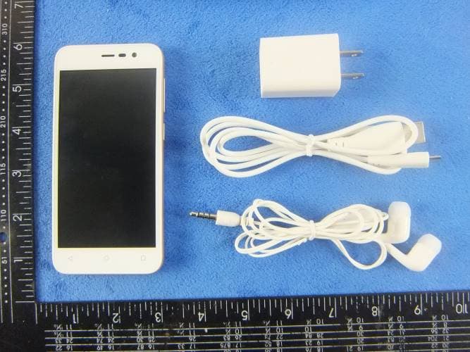
WA6S4512
Dec 23, 2015Mobile Phone
Equipment Class
DTS - Digital Transmission System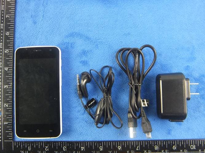
WA6SL4050
Dec 23, 2015Mobile Phone
Equipment Class
DTS - Digital Transmission System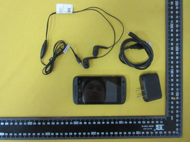
WA6S3502
Dec 07, 2015Mobile Phone
Equipment Class
DTS - Digital Transmission System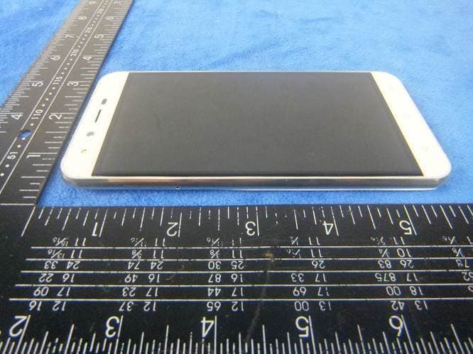
WA6SL5011
Dec 05, 2015Mobile Phone
Equipment Class
DTS - Digital Transmission System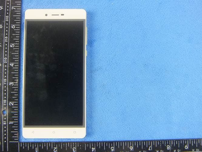
WA6SL6010
Nov 26, 2015Mobile Phone
Equipment Class
DTS - Digital Transmission System