WA6I725GSM/GPRS Quad-Band Mobile Phone
VeryKool USA Inc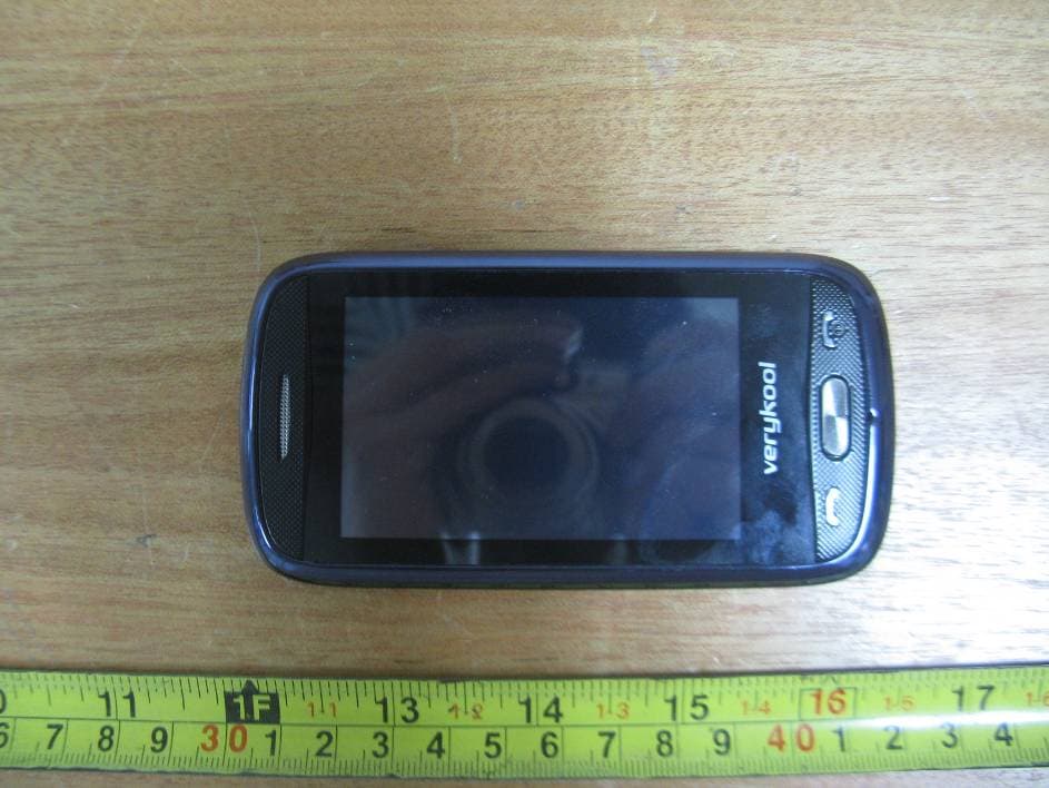
Click to zoom
Application Details
- Equipment Class
- PCE - PCS Licensed Transmitter held to ear
- Date of Grant
- Jul 31, 2011
- Application Purpose
- Original Equipment
- Date of Application
- Jul 31, 2011
- Equipment Note
- GSM/GPRS Quad-Band Mobile Phone
- Frequency Range
- 1850.20000000 - 1909.80000000
- Company
- VeryKool USA Inc
- Country
- United States
Documents & Files
Document Text
Text extracted from the exhibit documents filed with the FCC. Open a document above to read the original.
Users Manual
i725 User Manual Thank you for purchasing the i725 mobile phone Introduction Welcome to choose the i725 mobile phone. This user manual states the outstanding performance of the i725 mobile phone in detail. In addition to the basic call features, the i725 mobile phone and the system network also provide you with a variety of useful features and services to facilitate your work and leisure activities. The Company reserves the right to make any amendment on the technical specifications without any advance notice. Reading Statement for the Manual In manual, different typesetting styles are used to interpret different operating details, and the specific interpretation is as follows: Operation Description of Contents Example Showing contents Show with normal characters 0-9 General key All the keys except functional keys are shown by normal characters with frames 0-9 Functional key Functional key is shown with bold and frame OK Menu item Show in bold italics Hold a call Note: The picture shown in the manual are only used as function hint pictures which may be different from the ones shown in the mobile phone, and the ones in your mobile phone shall prevail. I CONTENT Introduction ............................................................................. I Security and performance..................................................... 1 1 Start Using ....................................................................... 4 1.1 Battery ........................................................................ 4 1.1.1 Uninstallation and installation of battery .............. 4 1.1.2 Charging the battery ............................................ 5 1.1.3 Use of battery ...................................................... 5 1.2 Side sliding keypad .................................................... 5 1.3 SIM card ..................................................................... 6 1.3.1 Insertion of SIM card ........................................... 7 1.3.2 Unlock the SIM card ............................................ 7 1.4 Plug and unplug the Memory card.............................. 8 1.5 Plug and unplug the earphone ................................... 8 1.6 Status bar and content ............................................... 8 1.6.1 Keys..................................................................... 9 1.6.2 Text input and edit window................................. 11 2 Dial and answer the call ............................................... 12 2.1 Making a call ............................................................ 12 2.1.1 Direct dial........................................................... 12 2.1.2 Making a call from the Phonebook list ............... 13 2.1.3 Speed dial.......................................................... 13 2.2 Answering a call ....................................................... 13 2.2.1 Answering new call ............................................ 13 2.2.2 Connecting two calls at the same time .............. 14 2.2.3 Conference call.................................................. 14 2.3 Emergency call......................................................... 14 3 Menu operation ............................................................. 15 4 Characteristic function ................................................. 16 4.1 Switch pages ............................................................ 16 4.2 Free-style menu ....................................................... 17 4.3 Change main menu icons’ position........................... 18 4.4 Curtain page ............................................................. 18 II 5 Phone............................................................................. 18 5.1 Phonebook ............................................................... 18 5.2 Call log ..................................................................... 20 5.3 Dialer ........................................................................ 20 5.4 Profiles ..................................................................... 20 5.5 File manager ............................................................ 21 5.6 Message................................................................... 21 5.7 Email ........................................................................ 22 5.8 Setting ...................................................................... 22 5.8.1 Time and date.................................................... 22 5.8.2 Language & Input method ................................. 22 5.8.3 Personalized settings ........................................ 22 5.8.4 LCD backlight .................................................... 23 5.8.5 Call settings ....................................................... 23 5.8.6 Network setup.................................................... 24 5.8.7 Security setup.................................................... 24 5.8.8 Wireless connect ............................................... 27 5.8.9 Phone mode settings ......................................... 28 5.8.10 Misc. settings..................................................... 28 5.8.11 Restore factory settings ..................................... 28 5.9 Image viewer ............................................................ 29 5.10 Camera .................................................................... 29 5.11 Calendar................................................................... 31 5.12 Alarm ........................................................................ 31 5.13 Media player............................................................. 31 5.14 Video recorder.......................................................... 32 5.15 Notes ........................................................................ 33 5.16 FM radio ................................................................... 33 5.17 Sound recorder......................................................... 34 5.18 Calculator ........…
Text truncated - open the document above for the full version.
Block Diagram
SYSTEM BLOCK DIAGRAM RF MODULE: SKY77552 CPU: MT6235B Transceiver: AD6548 Antenna LCD Module 2M camera T-flash Keypad FM Bluetooth Memory 26MHz CRYSTAL 32.768KHz CRYSTAL G-SENSOR GSM 850:824-849MHz (TX),869-894MHz (RX) PCS 1900:1850-1910MHz (TX),1930-1990MHz (RX) 2400 MHz -2483.5 MHz (TX/RX);
External Photos
EXHIBIT B - EUT EXTERNAL PHOTOGRAPHS EUT – Top View EUT – Bottom View EUT – Adapter View EUT – Adapter Label View
ID Label/Location Info
EXHIBIT A - FCC ID LABELING AND LOCATION FCC ID Label FCC ID Label Location Label here The label shown shall be permanently affixed at a conspicuous location on the device and be readily visible to the user at the time purchase (Labeling requirements per 2.925)
Internal Photos
EXHIBIT C - EUT INTERNAL PHOTOGRAPHS EUT – Battery off View EUT – Cover off View EUT – Main Board Top View GSM ant. BT ant. EUT – Main Board Bottom View EUT – Main Board Shield off Bottom View EUT – LCD Top View EUT – LCD Bottom View EUT – GSM Antenna View EUT – Battery View
Operational Description
i725 Circuit Description 1 RF circuit 1.1 Main functions of RF circuit: The baseband modulate the uplink signal, and then transmit it on RF carrier by the antenna; Demodulate the received wireless signal transmitted by the base station by the receiving circuit then get the forward signal; at the same time, provide the steady en-control 26MHz frequency source. 1.2 Structure of RF circuit: We can divide it to 4 units according to the functions: Antenna unit, frequency synthesized unit, receiving unit, transmitting unit. 1.2.1 Antenna unit Antenna unit is composed by antenna groupware, antenna switch and FEM SKY77552. This antenna groupware is the transceiver of the wireless signal that is composed by inside antenna, and could fetch up the disadvantages such as the low efficiency and the poor radiance direction by the high performance match. This phone has the antenna switch and diplexer. The antenna switch is used as the auto-test mechanical switch, which is located at the RF channel and parallel connected to the antenna. When producing and testing, it is connected to the test cable. Diplexer is used to isolate the received and transmitted signals, which can reduce the interference. 1.2.2 Frequency-synthesized unit The AD6548 has a single fast-locking fractional synthesizer used for VCO control in both receive and transmit mode. The entire system including VCO, tank, fractional N dividers, sigma delta compensation, charge pump and loop filters are fully integrated. The only external component is the frequency reference. The synthesizer is controlled via the serial interface. The VCO is fed into the respective dividers to generate the appropriate LO frequencies for the RX and TX bands. Fractional N Dividers The fractional N divider allows the PLL system to have a smaller step size than the comparison frequency which is set by the external reference to 26 MHz. This feature allows all the GSM frequency band raster to be achieved, with fast lock times and good phase noise characteristics. The divider section consists of a dual modulus 8/9 pre-scaler, integer M & A dividers, and fractional N system based on sigma-delta modulation to generate the required fractional divide ratio. The Denominator of the fractional divider can be set to 3 different values, (1040, 1170, 1235), depending on the mode of operation. For example a denominator of 1040 with an input fraction F maintains an average value of F/1040 allowing 25 kHz steps when operated at a reference of 26 MHz. Phase Frequency Detector/Charge Pump A Phase Frequency Detector (PFD) is used for the PLL phase detector. The charge pump is designed such that good matching of up and down currents is achieved over a wide output operating range. The charge pump output is internally routed to the integrated synthesizer loop filter. Synthesizer Loop filter To minimize complexity of the external PCB layout the Main Synthesizer loop filter is also fully integrated into the IC. No external components or adjustments are required. Voltage Controlled Oscillator The integrated voltage controlled oscillator (VCO) is a complete self- calibrating subsystem. This employs a fully auto-mated digital self- calibration function to ensure optimum phase noise performance over the entire frequency range. The VCO generates frequencies between 2520MHz and 2985MHz as required to operate in the four GSM bands for RX and TX. Reference Oscillator The AD6548 requires only an external low cost crystal as the frequency reference. The circuitry to oscillate the crystal and tune its frequency is fully integrated. For good noise immunity the oscillator is a balanced implementation requiring the crystal to be connected across 2 pins. There is a programmable capacitor array included for coarse tuning of fixed offsets (e.g. crystal manufacturing tolerance), and an integrated varactor for dynamic control. The oscillator is designed for use with a 26MHz crystal. 1.3. Transmitting unit The transmit section of the AD6548 radio implements a translation loop modulator. This consists of a quadrature modulator, high speed phase- frequency detector (PFD) with charge pump output, loop filter, TX VCO and a feedback down converting mixer. The VCO output (divided by 2 for low band) is fed to the power amplifier with a portion internally fed back into the down-converting feedback mixer to close the feedback loop. The Quadrature modulator takes the baseband I & Q signals and translates these into a GMSK signal at the Transmit Inter-mediate Frequency (TX IF). After bandpass filtering and limiting the TX IF signal is used as the reference input to the Phase Frequency Detector (PFD) of the transmit PLL. Phase Frequency Detector (PFD) The PFD ensures that the transmitted signal contains the required modulation and is accurately locked to the desired GSM channel. The downconverted feedback signal from the TX VCO and the Quadrature Modulator output are phase compared by the PFD. The PFD charge pump generates a current pulse proportional to the difference in phase which is applied to the loop filter. Loop filter To minimize complexity of the external PCB layout the TX loop filter is fully integrated into the IC. At power up the filter is automatically calibrated as part of the baseband filter cal, eliminating process tolerances. The calibration is fully integrated and requires no extra programming. TX VCO The Transmit Voltage Controlled Oscillator (TX VCO) and tank components are a fully integrated subsystem. The subsystem includes PA drivers so the outputs are used to directly drive the external PAs. The low noise oscillator design and internal filtering mean that external TX SAW filters are not required. In Low band operation the TX VCO output is divided by two and filtered. The TX VCO is automatically calibrated to ensure optimum performance over its operating frequency of 1648 to 1910 MHz. Feedback Down-Converting Mixer The feedback down converting mixer is used to translate the TX VCO output frequency …
Text truncated - open the document above for the full version.
Parts List/Tune Up Info
012345 1 * A210033V000 MainBoard PCBA 1 2 * P MR70023V000 MainBoard PCB 1 MR70023V000 Verykool 3 * P 0600003A001 res 0 +/-5% 0402 1/16W R412 R413 R414R615 R617 R902R911 R914 R915 C409 10 RC0402JR-070RL YAGEO 4 * P 0600003A018 res 4.7 +/-5% 0402 1/16W R411 1 RC0402JR-074R7L YAGEO 5 * P 0600003A026 res 10 +/-5% 0402 1/16W R606 1 RC0402JR-0710RL YAGEO 6 * P 0600003A030 res 15 +/-5% 0402 1/16W R108 1 RC0402JR-0715RL YAGEO 7 * P 0600003A043 res 51 +/-5% 0402 1/16W R618 1 RC0402JR-0751RL YAGEO 8 * P 0600003A044 res 56 +/-5% 0402 1/16W R607 1 RC0402JR-0756RL YAGEO 9 * P 0600003A058 res 220 +/-5% 0402 1/16W R220 R221 2 RC0402JR-07220RL YAGEO 10 * P 0600003A094 res 6K8 +/-5% 0402 1/16W R114 1 RC0402JR-076K8L YAGEO 11 * P 0600003A074 res 1K +/-5% 0402 1/16W R107 R201 R204R208 R211 R215R601 R611 R612 9 RC0402JR-071KL YAGEO 12 * P 0600003A078 res 1K5 +/-5% 0402 1/16W R203 R207 R209 3 RC0402JR-071K5L YAGEO 13 * P 0600003A082 res 2K2 +/-5% 0402 1/16W R602 R603 R604 R605 4 RC0402JR-072K2L YAGEO 14 * P 0600003A090 res 4K7 +/-5% 0402 1/16W R206 R507 R508 R512 R513 5 RC0402JR-074K7L YAGEO 15 * P 0600003A091 res 5K1 +/-5% 0402 1/16W R101 1 RC0402JR-075K1L YAGEO 16 * P 0600003A098 res 10K +/-5% 0402 1/16W R613 1 RC0402JR-0710KL YAGEO 17 * P 0600003A105 res 20K +/-5% 0402 1/16W R210 1 RC0402JR-0720KL YAGEO 18 * P 0600003A107 res 24K +/-5% 0402 1/16W R616 R116 2 RC0402JR-0724KL YAGEO 19 * P 0600003A114 res 47K +/-5% 0402 1/16W R701 R703 R704R705 R706 R908R909 R920 R702 9 RC0402JR-0747KL YAGEO 20 * P 0600003A115 res 51K +/-5% 0402 1/16W R301 1 RC0402JR-0751KL YAGEO 21 * P 0600003A118 res 68K +/-5% 0402 1/16W R213 1 RC0402JR-0768KL YAGEO 22 * P 0600003A122 res 100K +/-5% 0402 1/16W R105 R106 R404R407 R408 R409R501 R502 R713 R115 10 RC0402JR-07100KL YAGEO 23 * P 0600004A028 res 12 +/-1% 0402 1/16W R505 1 RC0402FR-0712RL YAGEO 24 * P 0600007A058 res 0.2 +/-1% 0805 1/8W R104 1 RL0805FR-070R2L YAGEO 25 * P 0600003A048 res 82 +/-5% 0402 1/16W C648 1 RC0402JR-0782RL Yageo 26 * P 0900037A001 Conn-BB s 60pin 0.4pitchH0.9 CONN503 1 DF30FC-60DS-0.4V(81) Hirose 27 * P 0900064A001 conn-switch 0.2mm 4.5×2.3×1.7 KEY701 KEY702 KEY703 3 LS10N2-T Citizen 28 * P 0900327A001 Conn-BB S 24pin 0.4pitch1.5mm CONN504CONN702 2 24 5602 024 000 829+ Kyocera Supplier P/N Supplier Name Main Board BOM Item Assy Level QTY Purchase Level Part No. Description Ref No. 012345 Supplier P/N Supplier Name Main Board BOM Item Assy Level QTY Purchase Level Part No. Description Ref No. 29 * P 0900600A001 MIN I/O 12PIN FEMALE0.5PITCH DIP+SMT TYPEH=2.0 CONN501 1 WKUBI008-001 JTCONN 30 * P 0900699A001 conn-TF holder H=1.95 CONN701 1 WKTFH010-S03 JTCONN 31 * P 2100005A041 Cap Ceramic 0402 6pF +/-0.1pF 50V C0G C632 1 UMK105CG060BW-F Taiyo Yuden 32 * P 2100005A045 Cap Ceramic 0402 6.8pF +/-0.25pF 50V C0G C903 1 UMK105CG6R8CW-F Taiyo Yuden 33 * P 2100005A046 Cap Ceramic 0402 7pF +/-0.25pF 50V C0G C618 C619 2 UMK105CG070CW-F Taiyo Yuden 34 * P 2100005A054 Cap Ceramic 0402 9pF +/-0.25pF 50V C0G C616 C617 2 UMK105CG090CV-F Taiyo Yuden 35 * P 2100005A062 Cap Ceramic 0402 12pF +/-5% 50V C0G C406 C150 C151C152 C153 C234C236 C530 C531C532 C533 C534C535 C536 C537C538 C539 C540C550 C551 C552C553 C554 C555C556 C557 C558C561 C562 C563C510 C511 C512C513 C514 C516C517 C520 C525C526 C527 C528 C529 43 UMK105CG120JV-F Taiyo Yuden 36 * P 2100005A066 Cap Ceramic 0402 18pF +/-5% 50V C0G C622 C623 2 UMK105CG180JV-F Taiyo Yuden 37 * P 2100005A126 Cap Ceramic 0402 8pF +/-0.25pF 50V C0G C620 C621 2 UMK105CG080CV-F Taiyo Yuden 38 * P 2100005A068 Cap Ceramic 0402 22pF +/-5% 50V C0G C101 C102 C631C633 C636 C637 R614 7 UMK105CG220JV-F Taiyo Yuden 39 * P 2100005A069 Cap Ceramic 0402 24pF +/-5% 50V C0G C808 1 UMK105CG240JV-F Taiyo Yuden 40 * P 2100005A070 Cap Ceramic 0402 27pF +/-5% 50V C0G C625 1 UMK105CG270JV-F Taiyo Yuden 41 * P 2100005A072 Cap Ceramic 0402 39pF +/-5% 50V C0G C606 C608 C624C231 C232 C233C215 C216 C227 C228 10 UMK105CG390JV-F Taiyo Yuden 42 * P 2100005A074 Cap Ceramic 0402 47pF +/-5% 50V C0G C602 1 UMK105CG470JV-F Taiyo Yuden 012345 Supplier P/N Supplier Name Main Board BOM Item Assy Level QTY Purchase Level Part No. Description Ref No. 43 * P 2100005A077 Cap Ceramic 0402 82pF +/-5% 50V C0G C607 C609 2 UMK105CG820JV-F Taiyo Yuden 44 * P 2100005A079 Cap Ceramic 0402 100pF +/-5% 50V C0G C209 C501 2 UMK105CG101JV-F Taiyo Yuden 45 * P 2100005A085 Cap Ceramic 0402 220pF +/-5% 50V C0G C217 C634 2 UMK105CG221JV-F Taiyo Yuden 46 * P 2100006A023 Cap Ceramic 0402 1000pF+/-10% 50V X7R C142 C604 C629 3 UMK105B7102KV-F Taiyo Yuden 47 * P 2100006A037 Cap Ceramic 0402 0.015uF+/-10% 16V X7R C218 1 EMK105B7153KV-F Taiyo Yuden 48 * P 2100006A039 Cap Ceramic 0402 0.022uF+/-10% 16V X7R C809 C813 2 EMK105B7223KV-F Taiyo Yuden 49 * P 2100006A042 Cap Ceramic 0402 0.033uF+/-10% 16V X7R C612 1 EMK105B7333KV-F Taiyo Yuden 50 * P 2100006A052 Cap Ceramic 0402 0.1uF +/-10% 16V X5R C108 C123 C125C127 C128 C130C132 C134 C136C137 C138 C139C143 C201 C204C210 C211 C229C301 C302 C405C518 C603 C605C610 C613 C614 32 EMK105BJ104KV-F Taiyo Yuden 51 * P 2100006A055 Cap Ceramic 0402 0.22uF+/-10% 10V X5R C611 1 LMK105BJ224KV-F Taiyo Yuden 52 * P 2100006A062 Cap Ceramic 0402 1uF +/-10% 10V X5R C103 C112 C117 C118 C119 C122C124 C140 C141C144 C149 C220C403 C404 C410C411 C505 C507 19 LMK105BJ105KV-F Taiyo Yuden 53 * P 2100010A071 Cap Ceramic 0603 1uF +/-10% 25V X5R C104 C504 2 TMK107BJ105KA-T Taiyo Yuden 54 * P 2100010A072 Cap Ceramic 0603 2.2uF +/-10% 6.3V X5R C120 C701 2 JMK107BJ225KA-T Taiyo Yuden 55 * P 2100010A076 Cap Ceramic 0603 4.7uF +/-10% 6.3V X5R C106 C107 C109C110 C111 C113C115 C133 C203 C905 C907 11 JMK107BJ475KA-T Taiyo Yuden 56 * P 2100011A026 Cap Ceramic 0603 10uF +/-20% 6.3V X5R C129 C135 C515 3 JMK107BJ106MA-T Taiyo Yuden 57 * P 2100014A051 Cap Ceramic 0805 10uF +/-10% 6.3V X5R T=0.95mmmax C145 C207 2 JMK212BJ106KD-T Taiyo Yuden 58 * P 2100015A029 Cap Ceramic 0805 22uF +/-20% 6.3V X5R C105 C202 C214 3 JMK212BJ226MG-T Taiyo Yuden 012345 Supplier P/N Supplier Name Main Board BOM Item Assy Level QT…
Text truncated - open the document above for the full version.
Parts List/Tune Up Info
Tune up procedure Tune up procedure shall be over the power range or at specific operating power levels. 1. It must provide an operational voltage (3.4 ~ 4.2V DC) to turn on the device and on one certain channel in service mode by means of company proprietary software. 2. Base station simulator (Agilent 8960) measures the GSM device specific RF characteristics. 3. The maximum gains of each individual device are adjusted until the target value met. z For GSM 850 band: PCL = 5, PWR = 33± 2dBm z For PCS 1900 band: PCL = 0, PWR = 30± 2dBm z For BLUETOOTH PWR = 0dBm Then these appropriate gain settings are stored in each device individually. The user has no possibility to change these settings later on, and during manufacturing each device will be individual calibrated. The measurement is done in fully calibrated setup, which is based on a Agilent 8960 base station simulator. Furthermore, the highest power level is verified afterwards in a call measurement on three channels (low, middle and high).
RF Exposure Info
Note: This test report is prepared for the customer shown above and for the device described herein. It may not be duplicated or used in part without prior written consent from Bay Area Compliance Laboratories Corp. This report must not be used by the customer to claim product certification, approval, or endorsement by NVLAP*, NIST, or any agency of the Federal Government. * This report contain data that are not covered by the NVLAP accreditation and are marked with an asterisk “★" (Rev.2) SAR EVALUATION REPORT For Verykool USA Inc. 4350 Executive Dr., #100, San Diego, CA 92121, USA FCC ID: WA6I725 Report Type: Original Report Product Type: GSM/GPRS Quad-band Mobile Phone Test Engineer: Cabin Hu Report Number: RSZ110522001-20 Report Date: 2011-07-30 Reviewed By: William Chen EMC Engineer Prepared By: Bay Area Compliance Laboratories Corp. (Shenzhen) 6/F, the 3rd Phase of WanLi Industrial Building, ShiHua Road, FuTian Free Trade Zone Shenzhen, Guangdong, China Tel: +86-755-33320018 Fax: +86-755-33320008 Bay Area Compliance Laboratories Corp. (Shenzhen) FCC ID: WA6I725 Report No.: RSZ110522001-20 Page 2 of 152 SAR Evaluation Report Attestation of Test Results Company NameVerykool USA Inc EUT DescriptionGSM/GPRS Quad-band Mobile Phone Model Numberi725 EUT Information Date of Test2011.07.28—2011.07.30 Band Max. SAR Level(s) Measured Limit (W/Kg) Cellular 0.541 W/kg, 1g Head Tissue 0.823 W/kg, 1g Body Tissue PCS 0.531 W/kg, 1g Head Tissue 0.510 W/kg, 1g Body Tissue 1. 6 ANSI/IEEE C95.1 : 1999 IEEE Standard for Safety Levels with Respect to Human Exposure to Radio Frequency Electromagnetic Fileds,3 kHz to 300 GHz. ANSI/IEEE C95.3 : 2002 IEEE Recommended Practice for Measurements and Computations of Radio Frequency Electromagnetic Fields With Respect to Human Exposure to SuchFields,100 kHz-300 GHz. OET BULLETIN 65 SUPPLEMENT C Evaluating Compliance with FCC Guidelines for Human Exposure To Radiofrequency Electromagnetic Fields. Applicable Standards IEEE 1528: 2003 IEEE Recommended Practice for Determining the Peak Spatial-Average Specific Absorption Rate (SAR) in the Human Head from Wireless Communications Devices: Measurement Techniques. Note: This wireless device has been shown to be capable of compliance for localized specific absorption rate (SAR) for General Population/Uncontrolled Exposure limits specified in ANSI/IEEE Standards and has been tested in accordance with the measurement procedures specified in FCC OET 65 Supplement C and IEEE 1528-2003. The results and statements contained in this report pertain only to the device(s) evaluated. Bay Area Compliance Laboratories Corp. (Shenzhen) FCC ID: WA6I725 Report No.: RSZ110522001-20 Page 3 of 152 SAR Evaluation Report TABLE OF CONTENTS DOCUMENT REVISION HISTORY .........................................................................................................................5 EUT DESCRIPTION ....................................................................................................................................................6 TECHNICAL SPECIFICATIONS.......................................................................................................................................6 REFERENCE, STANDARDS AND GUILDELINES ................................................................................................7 SAR LIMITS.................................................................................................................................................................8 FACILITIES AND ACCREDITATION .....................................................................................................................9 DESCRIPTION OF TEST SYSTEM ........................................................................................................................10 EQUIPMENT LIST AND CALIBRATION .............................................................................................................17 EQUIPMENTS LIST & CALIBRATION INFO...................................................................................................................17 SAR MEASUREMENT SYSTEM VERIFICATION ..............................................................................................18 LIQUID VERIFICATION...............................................................................................................................................18 SYSTEM ACCURACY VERIFICATION...........................................................................................................................21 SAR SYSTEM VALIDATION DATA .....................................................................................................................22 EUT TEST STRATEGY AND METHODOLOGY .................................................................................................30 TEST POSITIONS FOR DEVICE OPERATING NEXT TO A PERSON’S EAR........................................................................30 CHEEK/TOUCH POSITION...........................................................................................................................................31 EAR/TILT POSITION...................................................................................................................................................31 TEST POSITIONS FOR BODY-WORN AND OTHER CONFIGURATIONS..............................................................................32 SAR EVALUATION PROCEDURE.................................................................................................................................33 OUTPUT POWER VERIFICATION .......................................................................................................................34 TEST BLOCK DIAGRAM AND PROCEDURE..................................................................................................................34 TEST RESULTS...............................................................................................…
Text truncated - open the document above for the full version.
Test Report
Note: This test report is prepared for the customer shown above and for the equipment described herein. It may not be duplicated or used in part without prior written consent from Bay Area Compliance Laboratories Corp. This report must not be used by the customer to claim product certification, approval, or endorsement by NVLAP*, or any agency of the Federal Government. * This report contains data that are not covered by the NVLAP accreditation and are marked with an asterisk “★” (Rev.2) TEST REPORT For Verykool USA Inc. 4350 Executive Dr., #100, San Diego, CA 92121, USA FCC PART 22H, PART 24E FCC ID: WA6I725 Report Type: Original Report Product Type: GSM/GPRS Quad-band Mobile Phone Test Engineer: Leon Chen Report Number: RSZ110522001-00-22H&24E Report Date: 2011-06-29 Reviewed By: Merry Zhao EMC Engineer Test Laboratory: Bay Area Compliance Laboratories Corp. (Shenzhen) 6/F, the 3rd Phase of WanLi Industrial Building, ShiHua Road, FuTian Free Trade Zone Shenzhen, Guangdong, China Tel: +86-755-33320018 Fax: +86-755-33320008 www.baclcorp.com.cn Bay Area Compliance Laboratories Corp. (Shenzhen) FCC ID: WA6I725 Report No.: RSZ110522001-00-22H&24E Page 2 of 28 FCC Part 22H/24E Test Report TABLE OF CONTENTS GENERAL INFORMATION.......................................................................................................................................4 PRODUCT DESCRIPTION FOR EQUIPMENT UNDER TEST (EUT) .....................................................................................4 OBJECTIVE...................................................................................................................................................................4 RELATED SUBMITTAL(S)/GRANT(S).............................................................................................................................4 TEST METHODOLOGY..................................................................................................................................................4 TEST FACILITY.............................................................................................................................................................5 SYSTEM TEST CONFIGURATION ..........................................................................................................................6 JUSTIFICATION.............................................................................................................................................................6 EQUIPMENT MODIFICATIONS.......................................................................................................................................6 CONFIGURATION OF TEST SETUP.................................................................................................................................6 BLOCK DIAGRAM OF TEST SETUP................................................................................................................................6 SUMMARY OF TEST RESULTS ...............................................................................................................................7 FCC §1.1307 & §2.1093 - RF EXPOSURE INFORMATION ...................................................................................8 APPLICABLE STANDARD..............................................................................................................................................8 TEST RESULT...............................................................................................................................................................8 FCC §2.1047 - MODULATION CHARACTERISTIC ..............................................................................................9 FCC §2.1046, §22.913 (A) & §24.232 (C) - RF OUTPUT POWER.........................................................................10 APPLICABLE STANDARD............................................................................................................................................10 TEST PROCEDURE.......…
Text truncated - open the document above for the full version.
Contact Information
Applicant
Sunny Choi
Test Firm
Bay Area Compliance Laboratory Corp. (Shenzhen)John Chan
Technical Specifications
| # | Rule Parts | Frequency Range | Power Output | Emission | Tolerance |
|---|---|---|---|---|---|
| 2 | 24E | 1.85 GHz - 1.91 GHz | 533.00 mW | 250KGXW | 2.5 ppm |
Other Applications from VeryKool USA Inc
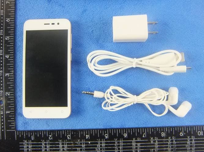
WA6S4512
Dec 23, 2015Mobile Phone
Equipment Class
DTS - Digital Transmission System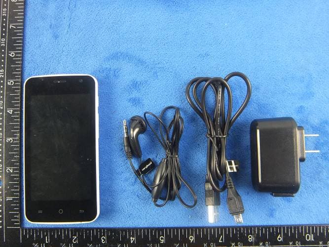
WA6SL4050
Dec 23, 2015Mobile Phone
Equipment Class
DTS - Digital Transmission System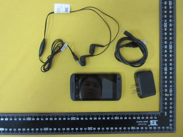
WA6S3502
Dec 07, 2015Mobile Phone
Equipment Class
DTS - Digital Transmission System
WA6SL5011
Dec 05, 2015Mobile Phone
Equipment Class
DTS - Digital Transmission System
WA6SL6010
Nov 26, 2015Mobile Phone
Equipment Class
DTS - Digital Transmission System