WA6S1353G MOBILE PHONE
VeryKool USA Inc
Click to zoom
Application Details
- Equipment Class
- DTS - Digital Transmission System
- Date of Grant
- Aug 05, 2012
- Application Purpose
- Original Equipment
- Date of Application
- Aug 05, 2012
- Equipment Note
- 3G MOBILE PHONE
- Frequency Range
- 2412.00000000 - 2462.00000000
- Company
- VeryKool USA Inc
- Country
- United States
Documents & Files
Document Text
Text extracted from the exhibit documents filed with the FCC. Open a document above to read the original.
Users Manual
1 Your new S135 will give you great productivity and fun. Use this quick guide to take advantage of all the features available to you. Welcome to register your new product. • This manual and SW of the phone are subject to changes by verykool USA Inc. without advance notice Welcome to verykool 2 Functions Description 1. Left soft key (LSK &SIM2 dial) 8. Receiver 2. Right soft key (RSK) 9. MIC 3. Send key (SIM1 dial)10. 3.5mm Earphone jack 4. End key (End), Power On/Off 11. USB socket &charging socket 5. OK key 12. Speaker 6. Navigation key 13. Camera lens 7. Keypad 3 1 2 3 4 Insert SIM card and T‐flash 4 Note: For Dual-SIM models, please select SIM1/SIM2 before proceeding. Make a call In the standby mode Input the number Press Snd key in single SIM mode End a call Press End key Add a new Enter Phonebook contact Scroll to the top and select Add new contact OK Select To SIM/To phone Choose the field to Edit Done When finished editing fields, select Done Send a text msgMessages Write message Once done typing press OK Enter recipient or add from phonebook or by hand OK With my verykool S135I want to... 5 Audio player Multimedia Audio player List Options Refresh list FM radio Multimedia FM radio Plug in your earphone Take a picture Camera Press OK key or 0 key to take pictures Turn on Settings Bluetooth Connectivity Bluetooth Power Select to switch on/off Bluetooth WLAN Search for networks Networks list Input pre-shared key WLAN WLAN Connected 3G WCDMA HSDPA 7.2Mbps; 6 HSUPA 5.76Mbps Accessories in Handset 1 pcs Package Battery 1 pcs Travel charger 1 pcs USB 1 pcs Earphone 1 pcs User manual 1 pcs Join the verykool zone! 7 Registering your new cell phone will take you less than 2 minutes and will give you access to the verykool zone where you will enjoy from promotions, ringtones, technical information, support and much more. Visit: www.verykoolzone.net Security and Performance Please read these safety guidelines before using your mobile phone to assure the safe and proper use of the phone. General ◆ Please turn off your mobile phone on an airplane, in the hospital or any location that may restrict mobile phone use—otherwise normal operation of electrical equipment and medical instruments may be affected. Please obey local regulations when using your mobile phone. ◆ While driving, please obey local laws and regulations regarding mobile phone use. When using your phone while driving, please obey the following rules: concentrate on driving and be aware of traffic conditions; use your mobile phone hands-free function; and under poor driving conditions, please stop the car before using your phone. ◆ Please obey laws, regulations and signs when 8 near an area storing fuel, chemicals, or other volatile materials. ◆ Please keep mobile phones, batteries, and chargers out of reach of children. ◆ Please do not use your mobile phone near low signal or precision electronic equipment. Radio wave interference may cause the malfunctioning of such electronic equipment and other problems. Special attention must be paid near the following equipment: hearing aids, pacemakers and other electronic medical equipment, smoke detectors, automatic doors and other automatic control installations. To find out the effect of mobile phones on a pacemaker or other electronic medical equipment please contact the manufacturers or local sales agents of the equipment. ◆ This mobile phone has an automatic “power on” function. Please refer to the mobile phone’s clock setting to ensure that the mobile phone will not automatically turn on during a plane flight. ◆ To prevent the mobile phone from malfunctioning or catching fire, please do not violently impact, jolt, or throw your mobile phone. ◆ Please do not place the battery, mobile phone, or charger in a microwave oven or high-pressure equipment. Subjecting the phone to these environments could lead to circuitry damage or a fire. ◆ Please do not use your mobile phone near 9 flammable or volatile gases, which may cause a malfunction or fire. ◆ Please do not subject your mobile phone to high temperatures, high humidity, or excessive dust, which could lead to malfunction. ◆ To prevent your mobile phone from falling, malfunctioning or being damaged, please do not place your phone on uneven or unstable surfaces. Phone Safety ◆ Do not disassemble or modify the mobile phone, as it could lead to damage such as battery leakage or circuitry failure. ◆ Please do not subject the LCD to impact or use the screen to strike things, as this will damage the LCD board and cause leakage of the liquid crystal. There is a risk of blindness if the liquid crystal chemicals get into the eyes. If this occurs, rinse eyes immediately with clear water (under no circumstances rub your eyes) and go immediately to a hospital for treatment. ◆ Under very rare circumstances, using the mobile phone in certain model cars may negatively affect the internal electronic equipment. In order to ensure your safety, under such circumstances please do not use the mobile phone. If your car is equipped with an airbag, please do not place your phone on top of it or within the contact area of the airbag in order to 10 avoid seriously harming the driver or passenger when the airbag inflates. ◆ Please do not use needles, pen tips, or other sharp objects on the keypad as this may damage the mobile phone or cause it to malfunction. ◆ Avoid letting your mobile phone come into close contact with magnetic objects such as credit cards and floppy disks, as the radiation produced by the phone may erase the information stored on these items. ◆ Please keep small metal objects such as thumbtacks far away from the receiver. When the receiver is in use, it becomes magnetic and may attract these small metal objects and may cause injury or damage to the mobile phone. ◆ Do not expose the mobile phone to humidity, water, or other liquids. If liquid enters the phone, short circuits, battery leaks and other malfunctions may occur. ◆ Please use the mob…
Text truncated - open the document above for the full version.
Cover Letter(s)
Shenzhen MORLAB Communication Technology Co., Ltd. Tel: +86 755 61281201 Fax: +86 755 86130218 3 F, Electronic Testing Building. Shahe Road, Xili, Nanshan Districe, Shenzhen, 518055 P R China Test Lab Attestation Letter Date of Test: 2012‐08‐01 Applicant Name: Verykool USA Inc FCC Id: WA6S135 Name of Engineer Performing Test: Zhu Zhan (Typed) Statement of Compliance: (Test Lab) declares that this Unit has been tested in accordance with the test method identified in this test report and that we observed it being tested. It also declares that the Unit complies with the relevant limits. All instrumentation and accessories used to test this unit for compliance to the indicated test method are calibrated regularly in accordance with ISO 17025:2005 requirements by laboratories accredited by A2LA, NVLAP, or ACLAS for the measurement parameters. The measurements were made at: (Test Lab Name) Shenzhen MORLAB Communication Technology Co., Ltd. (Address) 3 F, Electronic Testing Building. Shahe Road, Xili, Nanshan Districe, Shenzhen, 518055 P R China Test Lab Witness‐ Signature of Test Lab Witness: Full Name, Typed:Zhu Zhan Title of Witness:Test Engineer Email Address:Zhu [email protected] Phone No.:+86‐755‐36698585 M:\Master Documents\Test Lab_Authorization LetterRev 120703.doc Page 1 of 1
External Photos
Verykool USA Inc Model: S135 REPORT NO.: STR12078082I-1 FCC PART 22H&24E EXHIBIT 2 - EUT EXTERNAL PHOTOGRAPHS Model: S135 with Two SIM Card EUT View 1 EUT View 2 Verykool USA Inc Model: S135 REPORT NO.: STR12078082I-1 FCC PART 22H&24E EUT View 3 EUT View 4 Verykool USA Inc Model: S135 REPORT NO.: STR12078082I-1 FCC PART 22H&24E EUT View 5 EUT View 6 Verykool USA Inc Model: S135 REPORT NO.: STR12078082I-1 FCC PART 22H&24E EUT View 7 Model: S135 with One SIM Card EUT View 1 Verykool USA Inc Model: S135 REPORT NO.: STR12078082I-1 FCC PART 22H&24E EUT View 2 EUT View 3 Verykool USA Inc Model: S135 REPORT NO.: STR12078082I-1 FCC PART 22H&24E EUT View 4 EUT View 5 Verykool USA Inc Model: S135 REPORT NO.: STR12078082I-1 FCC PART 22H&24E EUT View 6 EUT View 7
ID Label/Location Info
Verykool USA Inc Model: S135 REPORT NO.: STR12078082I-1 FCC PART 22H&24E EXHIBIT 1- PRODUCT LABELING Proposed FCC ID Label Format FCC ID: WA6S135 This device complies with Part 15 of the FCC Rules. Operation is subject to the following two conditions: (1) This device may not cause harmful interference, and (2) this device must accept any interference received, including interference that may cause undesired operation. Specifications : Text is Black in color and justified. Labels are printed in indelible ink on permanent adhesive silk-screened onto the EUT or shall be affixed at a conspicuous location on the EUT. FCC ID Label Location
Internal Photos
Verykool USA Inc Model: S135 REPORT NO.: STR12078082I-1 FCC PART 22H&24E EXHIBIT 3 - EUT INTERNAL PHOTOGRAPHS Model: S135 with Two SIM Card EUT Housing and Board View 1 EUT Housing and Board View 2 Verykool USA Inc Model: S135 REPORT NO.: STR12078082I-1 FCC PART 22H&24E EUT Housing and Board View 3 Solder Board-Component View 1 Verykool USA Inc Model: S135 REPORT NO.: STR12078082I-1 FCC PART 22H&24E Solder Board-Component View 2 Solder Board-Component View 3 Verykool USA Inc Model: S135 REPORT NO.: STR12078082I-1 FCC PART 22H&24E Model: S135 with One SIM Card EUT Housing and Board View 1 EUT Housing and Board View 2 Verykool USA Inc Model: S135 REPORT NO.: STR12078082I-1 FCC PART 22H&24E EUT Housing and Board View 3 Solder Board-Component View 1 Verykool USA Inc Model: S135 REPORT NO.: STR12078082I-1 FCC PART 22H&24E Solder Board-Component View 2 Solder Board-Component View 3
Operational Description
CIRCUIT DESCRIPTION 1. Baseband RF Processor MT6276 is a CMU with ARM processor inside. It is containing built-in LDO,RFVCO, Mixer, Loopfilter, LNA, and programmable-gain amplifier, Demodulator and I/Q modulator etc. Serial data can get well communication and control with it. And the well characteristics VCXO, filter and high performance data dealing and controlling make it as a good IC for mobile design. 2. The PA enlargement is an amplifier for the modulation signal and enlarge the well signal for the mobile using .It supporting the GSM850 GSM900 DCS1800 PCS1900and Band2 Band5 protocol. The mobile is consisted with th e main part of MT6276 and MT5931A, and other I/O interface accessories. MT5931A is powered and supporting with the 26MHz VCXO. I/Q is also controlled with it and the phase signal is direct-converted to IF I/Q signals and enter to the filter and the programmable-gain amplifier. Also, the serial data interface is active and communicate with the RFVCO, then to the Mixer and loopfilter. As the modulation and demodulation with the MT5931A RF Processing, the GSM850 GSM900 DCS1800 PCS1900 and BAND2 BAND5signal enter into the impedance-matching network of the input ports of the PA and passing though the PA Enlargement for amplify. Then the enlarge signal run to the impedance-matching network of the output ports of the PA. Matching with the antenna circuit. The signal is transmitting out through the ANT. The receiving procedure is a revised direction as the transmitting procedure while is separated through ANT switch and monitor with the Serial data interface terminal.
Schematics
MSDC Close to MT6276 A B C D 54321 D C B A 12345 0402 R102 2M AL14 DL_I_P AM15 DL_I_N AP15 DL_Q_P AR16 DL_Q_N AK17 UL_I_P AJ18 UL_I_N AM17 UL_Q_P AL16 UL_Q_N AN22 APC AH19 AFC AP21 3G_TX_VGA AK19 3G_VBIAS AM25 BSI1_CLK AL22 BSI1_DATA AK23 BSI1_CS1/GP1/PD AN24 BSI1_CS0 AN26 BSI0_CLK AR28 BSI0_DATA AL26 BSI0_CS0 AP27 BSI0_CS1/GP2/PD AK29 BPI_BUS0 AG24 BPI_BUS1 AE24 BPI_BUS2 AM31 BPI_BUS3 AN32 BPI_BUS4 AJ28 BPI_BUS5 AL28 BPI_BUS6/GP7/PD AM29 BPI_BUS7/GP8/PD AL30 BPI_BUS8/GP10/PD AP31 BPI_BUS9/GP6/PD AR32 BPI_BUS10 AJ26 BPI_BUS11 AN28 BPI_BUS12 AR30 BPI_BUS13/GP5/PD AN30 BPI_BUS14/GP9/PD AM27 VM0/GP3/PD AP29 VM1/GP4/PD U101-A MT6276 0402 C101 18pF 0402 R104 0R 12 34 X101 SSP-T7 (32K) AM21 26M_CK_IN AR22 XOUT AP23 XIN AM23 TESTMODE AK21 RTC_GPIO/GP109/PD AP33 URXD1/GP11/PU AR34 UTXD1/GP12 AG30 MCU_JTRST_B/GP22/PD AJ32 MCU_JTCK/GP23/PU AE28 MCU_JTDI/GP24/PU AM35 MCU_JTMS/GP25/PU AD25 MCU_JTDO/GP26 AL34 MCU_JRTCK/GP27 AF29 SWCLKTCK/GP28/PU AK33 SWDIOTMS/GP29/PU E32 LSCK/GP70/PD G30 LSA0/GP71/PD D31 LSDA/GP72/PD G32 LSCE0B/GP73 B31 LSCE1B/GP74/PU AH27 URXD2/GP13/PU AN34 UTXD2/GP14 W4 USB_VBUS P1 USB_DM R2 USB_DP T7 USB_VRT U8 USB_ID U2 STXP V1 STXN V7 MPX AC30 SRCLKENA AH31 EINT0/GP33/PU AG32 EINT1/GP34/PU AF31 EINT2/GP35/PU AP35 DAICLK/GP15/PD AM33 DAIPCMOUT/GP16/PD AL32 DAIPCMIN/GP17/PD AG28 DAISYNC/GP18/PD AH29 DAIRST/GP19/PD AH33 PWMA/GP30/PD AK35 PWMB/GP31/PD AE26 PWMC/GP32/PD F31 LPCE1B/GP75/PU C30 LPCE0B D33 LPTE/GP76/PD C32 LRSTB E30 LRDB D35 LPA0 H29 LWRB AK31 EINT3/GP20/PU AF27 KCOL7/GP36/PU AJ34 KCOL6/GP37/PU AF33 KCOL5/GP38/PU AG34 KCOL4/GP39/PU AD29 KCOL3/GP40/PU AH35 KCOL2/GP41/PU AE30 KCOL1/GP42/PU AF35 KCOL0/GP43/PU AC28 KROW7/GP44 AE34 KROW6/GP45 AD31 KROW5/GP46 AE32 KROW4/GP47 AC32 KROW3/GP48 AD33 KROW2/GP49 AD35 KROW1/GP50 AC34 KROW0/GP51 R4 MC1CM0/GP101/PU M1 MC1DA0/GP102/PU M3 MC1DA1/GP103/PU L2 MC1CK/GP104/PU AL24 MC0INS/GP0/PU F1 MC2CM0/GP85/PU J8 MC2DA0/GP86/PU G4 MC2DA1/GP87/PU K7 MC2DA2/GP88/PU H1 MC2DA3/GP89/PU L6 MC2CK/GP90/PU K5 MC0CM0/GP92/PU J4 MC0DA0/GP93/PU M5 MC0DA1/GP94/PU K3 MC0DA2/GP95/PU L8 MC0DA3/GP96/PU M7 MC0CK/GP97/PU K1 MC0WP/GP99/PU P3 MC0RST/GP100 N6 MC1CK_FB/GP105/PU H3 MC2CK_FB/GP91/PU L4 MC0CK_FB/GP98/PU AP25 VDD28_FSRC AJ30 EINT4/GP21/PU U101-E MT6276 0402 C102 18pF 0402 C103 10nF 0402 R101 5.1K 1% 0402 R103 1M 0402 R105 0R TP3 TP4 F35 CMMCLK/GP69/PD G34 CMPCLK/GP68/PD N32 CMRST/GP54/PD M35 CMPDN/GP55/PD L34 CMVREF/GP56/PD M33 CMHREF/GP57/PD M31 CMDAT9/GP58/PD K35 CMDAT8/GP59/PD L30 CMDAT7/GP60/PD H35 CMDAT6/GP61/PD N30 SCL/GP52/PU N34 SDA/GP53/PU L32 CMDAT5/GP62/PD K33 CMDAT4/GP63/PD K31 CMDAT3/GP64/PD J34 CMDAT2/GP65/PD J32 CMDAT1/GP66/PD H33 CMDAT0/GP67/PD U101-I MT6276 VBUS VDD28_76 ASM_VCT1 ASM_VCT2 ASM_VCT3 ASM_VCT4 ASM_VDD BANDSW PAEN USB_VRT MCU_JRTCK MCU_JTDO MCU_JTMS MCU_JTDI MCU_JTCK MCU_JTRST_B AUDIO_PA_EN UMTSRX_IP UMTSRX_IN UMTSRX_QN UMTSRX_QP GSM_UMTSTX_IP GSM_UMTSTX_IN GSM_UMTSTX_QP GSM_UMTSTX_QN AFC VAPC W_PA_VBA 3G_TX_VGA BSI0_CS1 BSI0_DATA BSI0_CLK BSI1_CS0 BSI1_CLK BSI1_DATA BSI1_CS1 VCXOEN LPCE1B_WIFI LPCE0B_MAIN_LCM LPTE LRSTB LRDB LPA0 LSCE1B LWRB GPIO_WIFI_LDO_EN RTC_GPIO3 USB_DM USB_DP USB_VRT USB_ID VM0 VM1 EDGE_MODE BSI0_CS0 PWM0 EINT8 GPIO_CTP_PWR_EN EINT0 KCOL7 KCOL6 KCOL5 KCOL4 KCOL3 KCOL2 KCOL1 KCOL0 KROW7 KROW6 KROW5 KROW4 KROW3 KROW2 KROW1 KROW0 URXD1 UTXD1 URXD2 UTXD2 MC2DA3 MC2DA1 WIFI_EINT_B MC2DA0 GPIO_WIFI_RST MC0INS MC0CM0 MC0DA0 MC0DA1 MC0DA2 MC0DA3 MC0CK MC0WP MC0RST MC0CK_FB W_PA1_ON W_PA5_ON W_PA2_ON W_PA8_ON GPIO_GPS_32K SYSCLK LSA0 DAICLK MTK_WIFI_BT_PTA URXD3 UTXD3 GPIO_CAMPWR LSCK EINT2_WIFI EINT1 EINT3_GPS GPIO_GPS_SYNC SRCLKENAI_WIFI GPIO_CTP_SCL XOUT_BB 26M_CK_IN 32K_IN 32K_IN VBUS_BB 32K_OUT GND GND GND GND GND VUSB_76 MC1CK_FB CMDAT0 CMDAT1 SCL SDA CMDAT2 CMDAT3 CMDAT4 CMDAT5 CMMCLK CMVREF CMHREF CMDAT6 CMDAT7 CMDAT8 CMDAT9 CMPDN CMRST CMPCLK LC close to IC. (<10mm) ISENSE/BSTSNS 4mil differential to Rsense Keep at least 1 VIA1-2 each ball 40 mil 40 mil Start Connect to C211 Place between IC and IO port 40mil 40mil ©ñ¾aªñIC. (< 5mm) SIO1/2¤£¾aSCLK1/2®Ç SIO/SCLK trace 6mil 25mil 25mil Add Zenar Diode Place on the path from VBAT to IC (Battery connector or test point or IO connector) 25mil 25mil star connect to cap. (3mil) star connect to cap. (3mil) 15mil VIBRATOR Close to MT6276 1.8V IO for DDR 1.2V IO for DDR2 Close to MT6276 Close to MT6276 Close to IC 1.35V Close to IC C205 connect to pin AN10, and then via to GND REFN use own VIA connected to GND Plane star connect to cap. (3mil) star connect to cap. (3mil) star connect to cap. (3mil) star connect to cap. (3mil) star connect to cap. (3mil) 50~800 mA Digital LDO VPA Digital LDO 200 Digital LDO 1.2/0.9 400 10 Digital LDO 1.35 800 Charger Digital LDO Analog LDO 100 1.8 VCAMA 1.5/1.8/2.5/2.8/3/3.1/3.3 Digital LDO Buck 0.9~3.4 VRF18 Buck 2.8/3/3.3/2.5 Vcore Buck VRF 100 LED Buck 2.8 VTCXO 100 Buck/LDO 2.75 400 VCAMD Vout (V) 3.3100 2.8 VBT100 Imax (mA) VUSB 400 150 Analog LDO VDD28 100 1.3/1.5/1.8/2.5/2.8/3/3.3 Analog LDO VSIM2 Vaproc VIO18 250 VMC VIBR Analog LDO Digital LDO1001.8/3.0VSIM 1.3/1.5/1.8/2.5/2.8/3/3.3 1.5/1.8/2.5/2.8 302.5AVDD25Analog LDO 1.3/1.5/1.8/2.5/2.8/3/3.3200 1.3/1.5/1.8/2.5/2.8/3/3.3200 Close to MT6276 Close to MT6276 Close to MT6276 MSDC2 Power MSDC0 Power MSDC1 Power A B C D 54321 D C B A 2345 BATTERY CONNECTOR 40mil 40mil 40mil 40mil 40mil 4mil 4mil 40mil Charging 0402 C272 100nF(NC) 0402 C225 100nF 0402 C267 1uF L209LQM2HPN2R2MG0 0603 C259 2.2uF 0402 C255 100nF R210 1R 0402 C204 1uF 0603 C266 4.7uF (NC) 0402 C250 100nF(NC) 0402 C260 100nF 0402 C210 1uF (NC) 0603 C274 2.2uF 0402 C201 1uF L218NRH3012T4R7MN 0402 C214 1uF (NC) L204BLM18PG221SH1 0402 C258 1uF 0603 C226 2.2uF 0603 C205 10uF 0402 C253 100nF (NC) L214 0R 0402 C221 1uF 0402 C247 100nF 0402 C261 NC 0402 C203 1uF 0402 C271 1uF 0402 C216 1uF (NC) 0402 R230 0R (NC) 0402 C269 100nF L205LQM2HPN2R2MG0 0603 C230 4.7uF A K D201 UDZS5.1B L207BLM18PG221SH1 0402 R216 1k 0603 C217 2.2uF 0603 C254 2.2uF L212LQM2HPN2R2MG0 0402 C265 1uF 0402 L216 0R 0603 C229 4.7uF 0402 C249 100…
Text truncated - open the document above for the full version.
Test Setup Photos
Verykool USA Inc Model: S135 REPORT NO.: STR12078082I-2 FCC PART 15.247 EXHIBIT 4 - TEST SETUP PHOTOGRAPHS Spurious Radiation Test Setup (Below 30MHz) Spurious Radiation Test Setup (30MHz to 1G) Verykool USA Inc Model: S135 REPORT NO.: STR12078082I-2 FCC PART 15.247 Spurious Radiation Test Setup (Above1G)
Contact Information
Applicant
Sunny Choi
Test Firm
SEM.Test Compliance Service Co., Ltd.Jandy So
Technical Specifications
| # | Rule Parts | Frequency Range | Power Output |
|---|---|---|---|
| 1 | 15C | 2.41 GHz - 2.46 GHz | 38.00 mW |
Other Applications from VeryKool USA Inc
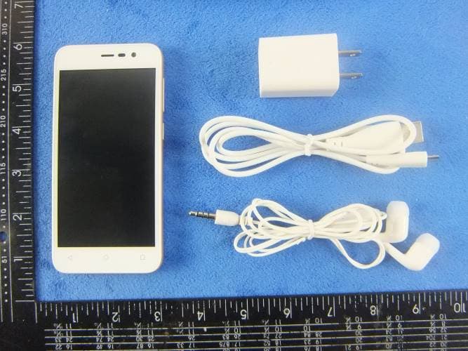
WA6S4512
Dec 23, 2015Mobile Phone
Equipment Class
DTS - Digital Transmission System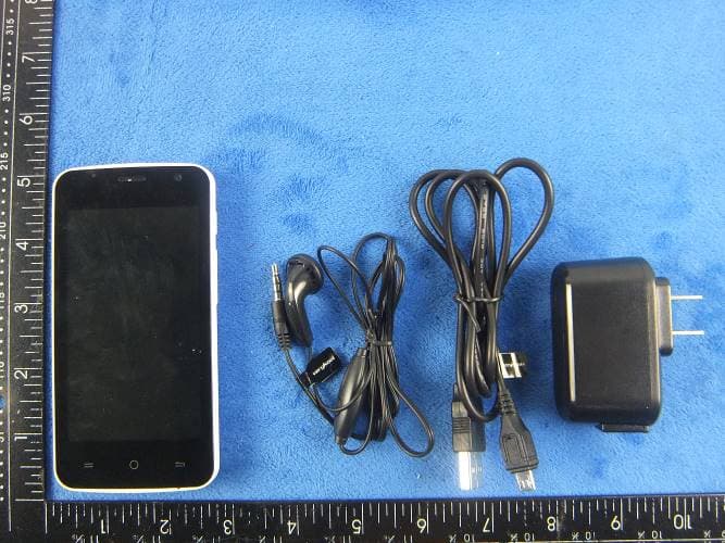
WA6SL4050
Dec 23, 2015Mobile Phone
Equipment Class
DTS - Digital Transmission System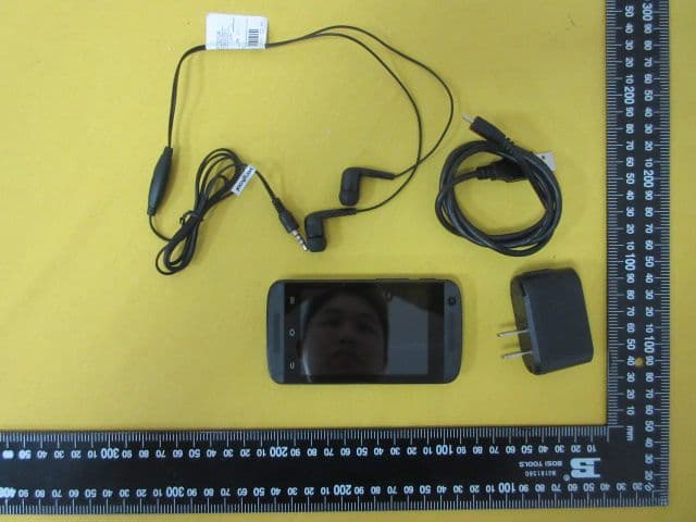
WA6S3502
Dec 07, 2015Mobile Phone
Equipment Class
DTS - Digital Transmission System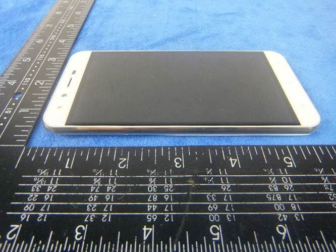
WA6SL5011
Dec 05, 2015Mobile Phone
Equipment Class
DTS - Digital Transmission System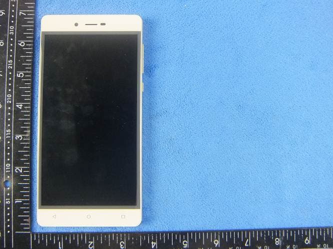
WA6SL6010
Nov 26, 2015Mobile Phone
Equipment Class
DTS - Digital Transmission System