WA6S350GSM/GPRS Dual-band Mobile Phone
VeryKool USA Inc
Click to zoom
Application Details
- Equipment Class
- DTS - Digital Transmission System
- Date of Grant
- Dec 27, 2012
- Application Purpose
- Original Equipment
- Date of Application
- Dec 27, 2012
- Equipment Note
- GSM/GPRS Dual-band Mobile Phone
- Frequency Range
- 2422.00000000 - 2452.00000000
- Company
- VeryKool USA Inc
- Country
- United States
Documents & Files
Document Text
Text extracted from the exhibit documents filed with the FCC. Open a document above to read the original.
Users Manual
S350 User Manual Thank you for purchasing the S350 mobile phone Introduction Welcome to choose the S350 mobile phone. This user manual states the outstanding performance of the S350 mobile phone in detail. In addition to the basic call features, the S350 mobile phone and the system network also provide you with a variety of useful features and services to facilitate your work and leisure activities. The Company reserves the right to make any amendment on the technical specifications without any advance notice. Reading Statement for the Manual In manual, different typesetting styles are used to interpret different operating details, and the specific interpretation is as follows: Operation Description of Contents Example Showing contents Show with normal characters 0-9 General key All the keys except functional keys are shown by normal characters with frames 0-9 Functional key Functional key is shown with bold and frame OK Menu item Show in bold Edit Note: The pictures shown in the manual are only used as function hint which may be different from the phone, and the ones in your phone shall prevail. I CONTENT INTRODUCTION................................................................. I SECURITY AND PERFORMANCE ................................... 1 1 START USING ............................................................ 3 1.1 BATTERY.........................................................3 1.2 SIM CARD.......................................................3 1.3 PLUG THE MEMORY CARD...................................3 1.4 PLUG THE EARPHONE.........................................4 1.5 KEYS...............................................................4 1.6 TEXT INPUT AND EDIT WINDOW...........................5 2 HOME SCREEN .......................................................... 5 2.1 CREATE HOME SCREEN SHORTCUTS AND WIDGETS...5 2.2 REMOVE ITEMS FROM THE HOME SCREEN..............5 2.3 MOVE OBJECTS ON THE HOME SCREEN..................5 2.4 NOTIFICATION AND CONNECTION STATUS ICONS......5 3 DIAL AND ANSWER THE CALL ................................ 5 3.1 DIALING A CALL.................................................5 3.2 ANSWERING A CALL...........................................6 3.3 EMERGENCY CALL..............................................6 4 DIALER ....................................................................... 7 5 MESSAGING & EMAIL ............................................... 7 5.1 MESSAGING.....................................................7 5.2 EMAIL.............................................................7 6 CONTACTS ................................................................. 8 7 BROWSER .................................................................. 9 8 SETTINGS ................................................................... 9 8.1 DUAL SIM SETTINGS..........................................9 II 8.2 WIRELESS & NETWORKS.....................................9 8.2.1 Wi‐Fi .......................................................9 8.2.2 Bluetooth..............................................10 8.2.3 Tethering & portable hotspot...............10 8.2.4 Mobile network settings.......................11 8.3 CALL SETTINGS...............................................11 8.4 SOUND.........................................................12 8.5 DISPLAY........................................................12 8.6 LOCATION & SECURITY.....................................13 8.7 APPLICATIONS................................................13 8.8 ACCOUNTS & SYNC.........................................14 8.9 PRIVACY........................................................14 8.10 SD CARD & PHONE STORAGE.............................14 8.11 LANGUAGE & KEYBOARD..................................15 8.12 VOICE INPUT & OUTPUT...................................15 8.13 ACCESSIBILITY.................................................15 8.14 DATE & TIME.................................................15 8.15 ABOUT PHONE................................................16 9 CAMERA, CAMCORDER & GALLERY ................... 16 9.1 CAMERA.......................................................16 9.2 VIDEO RECORDER...........................................16 9.3 GALLERY.......................................................17 10 MUSIC & VIDEO PLAYER ........................................ 17 11 TOOLS ...................................................................... 18 11.1 CALENDAR.....................................................18 III 11.2 ALARM CLOCK................................................19 11.3 CALCULATOR..................................................20 11.4 FILE MANAGER...............................................20 12 COMMON QUESTIONS ............................................ 21 13 MAINTENANCE GUIDELINE.................................... 22 14 FCC RF EXPOSURE INFORMATION AND STATEMENT ................................................................... 22 1 Security and performance ◆In thunder raining days, please do not use the mobile phone when charge it or outdoor, so as to avoid being struck by thunder or other injuries. ◆Please do not put the battery in high-temperature environment (high temperature will lead to heat of the battery upgrading), and keep the phone being charged and the charger away from people or other flammable and explosive articles in order to avoid fire, explosion or other dangers! ◆Please strictly adhered to the rules and do shut down the mobile phone on occasions which use of mobile phone is prohibited! ◆Please do not arbitrarily refit or teardown the phone and accessories. Only the authorized organizations can repair the phone. ◆Please do not use batteries, charger or accessories of non-standard original models. ◆Please do not join the two poles of the battery, so as not to result in battery short-circuit. ◆Please do not use the mobile phone when driving. In case of emergency, please use hand-free devices (which may be bought separatel…
Text truncated - open the document above for the full version.
Block Diagram
SYSTEM BLOCK DIAGRAM RF MODULE: RF7182 CPU: SC6820 Transceiver: SR1019 Antenna LCD Module 2M camera T-flash Keypad SIM WIFI+BT+FM CHIP: BCM4330 Memory 26MHz CRYSTAL 32.768KHz CRYSTAL WIFI/ BT Antenna FM Antenna GSM850/1900 BT2402-2480MHz,WiFi2412-2462MHz
External Photos
Verykool USA Inc Model: S350 REPORT NO.: STR12128073I-1 FCC PART 22H & 24E EXHIBIT 2 - EUT EXTERNAL PHOTOGRAPHS EUT View 1 EUT View 2 Verykool USA Inc Model: S350 REPORT NO.: STR12128073I-1 FCC PART 22H & 24E EUT View 3 EUT View 4 Verykool USA Inc Model: S350 REPORT NO.: STR12128073I-1 FCC PART 22H & 24E EUT View 5 EUT View 6 Verykool USA Inc Model: S350 REPORT NO.: STR12128073I-1 FCC PART 22H & 24E EUT View 7
ID Label/Location Info
Verykool USA Inc Model: S350 REPORT NO.: STR12128073I-1 FCC PART 22H & 24E EXHIBIT 1- PRODUCT LABELING Proposed FCC ID Label Format FCC ID: WA6S350 Specifications : Text is Black in color and justified. Labels are printed in indelible ink on permanent adhesive silk-screened onto the EUT or shall be affixed at a conspicuous location on the EUT. Proposed Label Location on EUT FCC ID Label Location
Internal Photos
Verykool USA Inc Model: S350 REPORT NO.: STR12128073I-1 FCC PART 22H & 24E EXHIBIT 3 - EUT INTERNAL PHOTOGRAPHS EUT Housing and Board View 1 EUT Housing and Board View 2 Verykool USA Inc Model: S350 REPORT NO.: STR12128073I-1 FCC PART 22H & 24E EUT Housing and Board View 3 Solder Board-Component View 1 Verykool USA Inc Model: S350 REPORT NO.: STR12128073I-1 FCC PART 22H & 24E Solder Board-Component View 2 Antenna View 1: Ant. GSM850/1900 Verykool USA Inc Model: S350 REPORT NO.: STR12128073I-1 FCC PART 22H & 24E Antenna View 2: Ant. WiFi/BT
Operational Description
S350 Circuit Description 1 RF circuit 1.1 Main functions of RF circuit: The baseband modulate the uplink signal, and then transmit it on RF carrier by the antenna; Demodulate the received wireless signal transmitted by the base station by the receiving circuit then get the forward signal; at the same time, provide the steady en-control 26MHz frequency source. 1.2 Structure of RF circuit: We can divide it to 4 units according to the functions: Antenna unit, frequency synthesized unit, receiving unit, transmitting unit. 1.2.1 Antenna unit Antenna unit is composed by antenna groupware, antenna switch and FEM RF7182. This antenna groupware is the transceiver of the wireless signal that is composed by inside antenna, and could fetch up the disadvantages such as the low efficiency and the poor radiance direction by the high performance match. This phone has the antenna switch and diplexer. The antenna switch is used as the auto-test mechanical switch, which is located at the RF channel and parallel connected to the antenna. When producing and testing, it is connected to the test cable. Diplexer is used to isolate the received and transmitted signals, which can reduce the interference. 1.2.2 Frequency-synthesized unit The SR1019 has a single fast-locking fractional synthesizer used for VCO control in both receive and transmit mode. The entire system including VCO, tank, fractional N dividers, sigma delta compensation, charge pump and loop filters are fully integrated. The only external component is the frequency reference. The synthesizer is controlled via the serial interface. The VCO is fed into the respective dividers to generate the appropriate LO frequencies for the RX and TX bands. Fractional N Dividers The fractional N divider allows the PLL system to have a smaller step size than the comparison frequency which is set by the external reference to 26 MHz. This feature allows all the GSM frequency band raster to be achieved, with fast lock times and good phase noise characteristics. The divider section consists of a dual modulus 8/9 prescaler, integer M & A dividers, and fractional N system based on sigma-delta modulation to generate the required fractional divide ratio. The Denominator of the fractional divider can be set to 3 different values, (1040, 1170, 1235), depending on the mode of operation. For example a denominator of 1040 with an input fraction F maintains an average value of F/1040 allowing 25 kHz steps when operated at a reference of 26 MHz. Phase Frequency Detector/Charge Pump A Phase Frequency Detector (PFD) is used for the PLL phase detector. The charge pump is designed such that good matching of up and down currents is achieved over a wide output operating range. The charge pump output is internally routed to the integrated synthesizer loop filter. Synthesizer Loop filter To minimize complexity of the external PCB layout the Main Synthesizer loop filter is also fully integrated into the IC. No external components or adjustments are required. Voltage Controlled Oscillator The integrated voltage controlled oscillator (VCO) is a complete self- calibrating subsystem. This employs a fully auto-mated digital self- calibration function to ensure optimum phase noise performance over the entire frequency range. The VCO generates frequencies between 2520MHz and 2985MHz as required to operate in the four GSM bands for RX and TX. Reference Oscillator The SR1019 requires only an external low cost crystal as the frequency reference. The circuitry to oscillate the crystal and tune its frequency is fully integrated. For good noise immunity the oscillator is a balanced implementation requiring the crystal to be connected across 2 pins. There is a programmable capacitor array included for coarse tuning of fixed offsets (e.g. crystal manufacturing tolerance), and an integrated varactor for dynamic control. The oscillator is designed for use with a 26MHz crystal. 1.3. Transmitting unit The transmit section of the SR1019 radio implements a translation loop modulator. This consists of a quadrature modulator, high speed phase- frequency detector (PFD) with charge pump output, loop filter, TX VCO and a feedback down converting mixer. The VCO output (divided by 2 for low band) is fed to the power amplifier with a portion internally fed back into the down-converting feedback mixer to close the feedback loop. The Quadrature modulator takes the baseband I & Q signals and translates these into a GMSK signal at the Transmit Inter-mediate Frequency (TX IF). After bandpass filtering and limiting the TX IF signal is used as the reference input to the Phase Frequency Detector (PFD) of the transmit PLL. Phase Frequency Detector (PFD) The PFD ensures that the transmitted signal contains the required modulation and is accurately locked to the desired GSM channel. The downconverted feedback signal from the TX VCO and the Quadrature Modulator output are phase compared by the PFD. The PFD charge pump generates a current pulse proportional to the difference in phase which is applied to the loop filter. Loop filter To minimize complexity of the external PCB layout the TX loop filter is fully integrated into the IC. At power up the filter is automatically calibrated as part of the baseband filter cal, eliminating process tolerances. The calibration is fully integrated and requires no extra programming. TX VCO The Transmit Voltage Controlled Oscillator (TX VCO) and tank components are a fully integrated subsystem. The subsystem includes PA drivers so the outputs are used to directly drive the external PAs. The low noise oscillator design and internal filtering mean that external TX SAW filters are not required. In Low band operation the TX VCO output is divided by two and filtered. The TX VCO is automatically calibrated to ensure optimum performance over its operating frequency of 1648 to 1910 MHz. Feedback Down-Converting Mixer The feedback down converting mixer is used to translate the TX VCO output frequency to …
Text truncated - open the document above for the full version.
Parts List/Tune Up Info
1 PCB MainBoard PCBA 1 2 PCB MainBoard PCB 1 3 Resistance res,0,+/-5%,0402,1/16W L604 L820 R101 R108 R313 R401 R408 R422 R423R601 R603 R611 R821 R838 R839 R840 R841R608 18 4 Resistance res,12,+/-5%,0402,1/16W R210 R211 2 5 Resistance res,33,+/-5%,0402,1/16W R110 R111 R212 R213 R415 R416 6 6 Resistance res,51,+/-5%,0402,1/16W R107 1 7 Resistance res,510,+/-5%,0402,1/16W R201 R204 2 8 Resistance res,1K,+/-5%,0402,1/16W R102 R207 R214 R227 R314 R801 R802 R803 8 9 Resistance res,1K5,+/-5%,0402,1/16W R202 R203 R604 3 10 Resistance res,2K,+/-5%,0402,1/16W R208 1 11 Resistance res,4K7,+/-5%,0402,1/16W R701 1 12 Resistance res,6K2,+/-5%,0402,1/16W R309 1 13 Resistance res,20K,+/-5%,0402,1/16W R218 1 14 Resistance res,22K,+/-5%,0402,1/16W R817 1 15 Resistance res,100K,+/-5%,0402,1/16W R219 R843 R844 3 16 Resistance res,220K,+/-5%,0402,1/16W R311 1 17 Resistance res,10M,+/-5%,0402,1/16W R310 1 18 Resistance res,43.2,+/-1%,0402,1/16W R312 1 19 Resistance res,15K,+/-1%,0402,1/16W R815 1 20 Resistance res, 0.36,+/-1%,0805,1/8W R407 1 21 Capacitance Cap,Ceramic,0402,3.9pF,+/-0.1p,50V,C0G C621 1 22 Capacitance Cap,Ceramic,0402,2.2pF,+/-0.1pF,50V,C0G C616 C617 C625 C626 4 23 Capacitance Cap,Ceramic,0402,2pF,+/-0.1pF,50V,C0G C622 1 24 Capacitance Cap,Ceramic,0402,3.3pF,+/-0.25pF,50V,C0G C634 C635 C812 C813 4 25 Capacitance Cap,Ceramic,0402,1.5pF,+/-0.1pF,50V,C0G C623 C624 2 26 Capacitance Cap,Ceramic,0402,8.2pF,+/-0.25pF,50V,C0G C809 1 27 Capacitance Cap,Ceramic,0402,10pF,+/-0.5pF,50V,C0G C807 C810 C814 C815 C816 C893 6 28 Capacitance Cap,Ceramic,0402,12pF,+/-5%,50V,C0G R811 R849 2 29 Capacitance Cap,Ceramic,0402,18pF,+/-5%,50V,C0G C717 C718 C719 C720 C781 C788 6 30 Capacitance Cap,Ceramic,0402,22pF,+/-5%,50V,C0G C302 C303 C602 C633 4 S350 QTY Description Ite m Name Ref No. 第 1 页,共 4 页 S350 QTY Description Ite m Name Ref No. 31 Capacitance Cap,Ceramic,0402,27pF,+/-5%,50V,C0G C101 C401 C403 C507 C604 C643 C644 C645C646 9 32 Capacitance Cap,Ceramic,0402,47pF,+/-5%,50V,C0G C203 C205 C206 C211 C212 C213 C214 C217C220 C407 C413 C631 C632 C639 C642 15 33 Capacitance Cap,Ceramic,0402,56pF,+/-5%,50V,C0G C636 1 34 Capacitance Cap,Ceramic,0402,100pF,+/-5%,50V,C0G C209 C219 C225 C229 C235 C317 6 35 Capacitance Cap,Ceramic,0402,470pF,+/-5%,50V,X7R C310 C657 2 36 Capacitance Cap,Ceramic,0402,1000pF,+/-5%,50V,X7R C227 C228 C230 C231 C612 C808 6 37 Capacitance Cap,Ceramic,0402,0.01uF,+/-10%,16V,X7R C232 C306 C431 C459 C461 C501 C503 7 38 Capacitance Cap,Ceramic,0402,0.022uF,+/-10%,16V,X7R C201 C202 C207 C208 4 39 Capacitance Cap,Ceramic,0402,0.1uF,+/-10%,16V,X5R C210 C308 C311 C414 C416 C417 C418 C419C421 C422 C423 C424 C425 C426 C428 C432C434 C502 C504 C506 C641 C704 C725 C802C803 C804 C821 C889 C894 29 40 Capacitance Cap,Ceramic,0402,0.22uF,+/-10%,10V,X5R C805 C806 C891 C895 C896 5 41 Capacitance Cap,Ceramic,0402,1uF,+/-10%,6.3V,X5R C619 C305 C312 C402 C404 C420 C443 C444C445 C446 C447 C449 C452 C453 C454 C456C458 C611 C613 C701 C702 C711 C713 C714C724 C836 C316 27 42 Capacitance Cap,Ceramic,0603,1uF,+/-10%,25V,X5R C409 1 43 Capacitance Cap,Ceramic,0603,2.2uF,+/-10%,6.3V,X5R C204 C427 C440 C450 C451 C455 C457 C466C505 C898 10 44 Capacitance Cap,Ceramic,0603,4.7uF,+/-10%,6.3V,X5R C429 C433 C435 C800 C801 C890 C892 C899 8 45 Capacitance Cap,Ceramic,0603,10uF,+/-20%,6.3V,X5R C233 C309 C430 C436 C438 C441 C442 C897 8 第 2 页,共 4 页 S350 QTY Description Ite m Name Ref No. 46 Capacitance Cap,Ceramic,0402,33pF,+/-5%,50V,C0G C481 1 47 Capacitance Cap,Ceramic,0805,10uF,+/-10%,6.3V,X5R, T=0.95mm max C415 1 48 Capacitance Cap,Ceramic,0201,33pF,+/-5%,25V,C0G C477 C478 2 49 Capacitance Cap,Ceramic,0805,22uF,+/-20%,6.3V,X5R,T=0.95mm max C215 C216 2 50 Capacitance Cap Ceramic 0805 22uF +/-20% 6.3V X5R C304 1 51 Inductance ind,1.5n,+/-0.3n,0402 L815 1 52 Inductance ind,2.4n,+/-0.3n,0402 L623 1 53 Inductance ind,3.3n,+/-0.3n,0402 L622 1 54 Inductance ind,5.6n,+/-0.3n,0402 L615 L616 2 55 P ind,10n,+/-5%,0402 L601 1 56 P ind,22n,+/-5%,0402 L611 L612 2 57 P ind,coil,4.3n,+/-0.3,0402 L621 1 58 P IND POWER;2.2uH;20%;3015;1.6A;1.6A 0.06ohm L810 1 59 P IND POWER;4.7uH;20%;2520;1.25A;0.84A 0.29ohm L401 L402 2 60 P Ferrite Bead,0402,75Ohm@100MHz,0.3Ohm DCR,600mA L811 L812 L813 L814 L831 R205 R206 R209 8 61 P Ferrite Bead,0402,1800Ohm@100MHz,1.8Ohm DCR,50mA L201 L202 L203 L210 4 62 Resistance EMI bead,1channel,220ohm@100MHz,0.55ohm(max)@DC,500mA,0603 R215 R216 R225 R226 4 63 Capacitance Cap,Tan,33uF,+/-20% ,6.3V C640 1 64 Diode Bi direction ESD Protection diode D801 D802 D803 D804 4 65 Diode esd, SOD-523,240w Peak pules power D402 1 66 Crystal Crystal, 32.768KHz, +/-20ppm, 12.5pF, 7.0*1.5*1.4(mm) OSC301 1 67 Crystal Crystal, 26MHz , 8PF +/-10ppm SMD SEAM SEALING3.2*2.5(mm) OSC801 OSC601 2 68 IC P-Channel 1.8v(G-S) MOSFET WIith Schottky Diode,1206-8 ChipFET U401 1 69 IC 4Gb (256Mb x16) NAND Flash+ 2Gb (64Mb x32) mobile DDR, DDR400,137Ball FBGA, 10.5mm*13m*1.2 U501 1 70 IC 1800/1900MHz range SAW filter for communication equipment. U604 1 71 IC Bluetooth BAND PASS FILTER U803 1 72 IC SAW Filter, 881.5/942.5MHz U603 1 73 IC BCM4330 WLAN + BT 2.1 + FM RX U801 1 74 IC Dual SPDT Analog Switch with Chip Scale Packaging U201 1 75 IC ±16 g 3-Axis Accelerometer with Digital Output (I2C), 2mm x 2mm x 0.95mmDFN package. U711 1 76 IC EMI FILTER U701 U702 U703 U704 U705 U706 6 77 IC RF PA;Quad Band GPRS/EDGE TRANSMIT MODULE, RF7182 U602 1 第 3 页,共 4 页 S350 QTY Description Ite m Name Ref No. 78 IC CPU SC6820 U101 1 79 IC PHEMT GaAs IC SP3T Switch 0.1–6.0 GHz U802 1 80 IC Transceiver, SR1019 U601 1 81 Antenna 2.4GHz BLUETOOTH CHIP ANTENNA. ANT801 1 82 Connector battery connector H1.2mm CONN402 1 83 Connector Micro USB conn 5pin CONN703 1 84 Connector Conn-ZIF,39pin,0.3pitch,f,H1.0 CONN702 1 85 Connector Conn-ZIF, 6pin, 0.5pitch, f(lock to front) H0.93 CONN704 1 86 Connector conn-sim Holder,bridge,H1.8 CONN404 1 87 Connector Conn_SIM holder,bridge,H1.5 CONN403 1 88 Connector conn-T-flash,11.4X5.5,H3.0 CONN701 1 89 Connector 3.5 AUDIO JACK CONN201 1 90 Antenna SMT_S…
Text truncated - open the document above for the full version.
Parts List/Tune Up Info
Tune up procedure Tune up procedure shall be over the power range or at specific operating power levels. It must provide an operational voltage (3.3 ~ 4.2V DC) to turn on the device and on one certain channel in service mode by means of company proprietary software. Base station simulator (Agilent 8960 ) measures the 2G device specific RF characteristics. The maximum gains of each individual device are adjusted until the target value met. Maximum RF Output Power Frequency Bands Service PCL/Class Target Value (Power) GSM 5 (Class 4) 32.19 ± 0.5dBm GPRS with 1 slot 5 (Class 4) 32.17 ± 0.5dBm GPRS with 2 slot 5 (Class 4) 30.53 ± 0.5dBm GPRS with 3 slot 5 (Class 4) 28.73 ± 0.5dBm GSM850 GPRS with 4 slot 5 (Class 4) 26.59 ± 0.5dBm GSM 0 (Class 1) 29.25 ± 0.5dBm GPRS with 1 slot 0 (Class 1) 29.25 ± 0.5dBm GPRS with 2 slot 0 (Class 1) 28.03 ± 0.5dBm GPRS with 3 slot 0 (Class 1) 25.71 ± 0.5dBm PCS1900 GPRS with 4 slot 0 (Class 1) 23.75 ± 0.5dBm 2.GHz 802.11b/gn / 13.28 ± 1.5dBm Then these appropriate gain settings are stored in each device individually. The user has no possibility to change these settings later on, and during manufacturing each device will be individual calibrated. The measurement is done in fully calibrated setup, which is based on a Agilent 8960 base station simulator. Furthermore, the highest power level is verified afterwards in a call measurement on three channels (low, middle and high).
RF Exposure Info
Report No.: 12CS027R-HP-US-P03V01 Page: 1 of 131 SAR Test Report Product Name : GSM/GPRS Dual-band Mobile Phone Model No. : S350 FCC ID : WA6S350 Applicant : Verykool USA Inc Address : 3636 Nobel Drive, Suite 325, San Diego, CA 92122 USA Date of Receipt : 11/12/2012 Date of Test : 18/12/2012 Issued Date : 19/12/2012 Report No. : 12CS027R-HP-US-P03V01 Report Version : V 2.3 The test results relate only to the samples tested. The test report shall not be reproduced except in full without the written approval of QuieTek Corporation. Report No.: 12CS027R-HP-US-P03V01 Page: 2 of 131 Test Report Certification Issued Date: 19/12/2012 Report No.: 12CS027R-HP-US-P03V01 Product Name : GSM/GPRS Dual-band Mobile Phone Applicant : Verykool USA Inc Address : 3636 Nobel Drive, Suite 325, San Diego, CA 92122 USA Manufacturer : Verykool Wireless Technology Ltd. Address : Room 1701, Reward Building C, No.203, 2nd Section of WangJing, Li Ze Zhong Yuan, ChaoYang District, Beijing, China Model No. : S350 FCC ID : WA6S350 Brand Name : verykool EUT Voltage : DC 3.7V Applicable Standard : FCC Oet65 Supplement C June 2001 IEEE Std. 1528-2003,47CFR § 2.1093 Test Result : Max. SAR Measurement (1g) Head: 0.257 W/kg Body: 0.817 W/kg Performed Location : Suzhou EMC Laboratory No.99 Hongye Rd., Suzhou Industrial Park Loufeng Hi-Tech Development Zone., Suzhou, China TEL: +86-512-6251-5088 / FAX: +86-512-6251-5098 FCC Registration Number: 800392 Documented By : (Engineering ADM: Alice Ni) Reviewed By : (Engineering Supervisor: Robin Wu) Approved By : (Manager: Marlin Chen) Report No.: 12CS027R-HP-US-P03V01 Page: 3 of 131 Laboratory Information We, QuieTek Corporation, are an independent EMC and safety consultancy that was established the whole facility in our laboratories. The test facility has been accredited/accepted(audited or listed) by the following related bodies in compliance with ISO 17025, EN 45001 and specified testing scope: The related certificate for our laboratories about the test site and management system can be downloaded from QuieTek Corporation’s Web Site :http://www.quietek.com/tw/ctg/cts/accreditations.htm The address and introduction of QuieTek Corporation’s laboratories can be founded in our Web site : http://www.quietek.com/ If you have any comments, Please don’t hesitate to contact us. Our contact information is as below: HsinChu Testing Laboratory : No.75-2, 3 rd Lin, Wangye Keng, Yonghxing Tsuen, Qionglin Shiang, Hsinchu County 307, Taiwan, R.O.C. TEL:+886-3-592-8858 / FAX:+886-3-592-8859 E-Mail : [email protected] LinKou Testing Laboratory : No.5-22, Ruishukeng, Linkou Dist., New Taipei City 24451, Taiwan, R.O.C. TEL : 886-2-8601-3788 / FAX : 886-2-8601-3789 E-Mail : [email protected] Suzhou Testing Laboratory : No.99 Hongye Rd., Suzhou Industrial Park Loufeng Hi-Tech Development Zone., SuZhou, China TEL : +86-512-6251-5088 / FAX : 86-512-6251-5098 E-Mail : [email protected] Taiwan R.O.C. : BSMI, NCC, TAF Germany : TUV Rheinland Norway : Nemko, DNV USA : FCC, NVLAP Japan : VCCI China : CNAS Report No.: 12CS027R-HP-US-P03V01 Page: 4 of 131 TABLE OF CONTENTS Description Page 1. General Information ................................................................................................. 6 1.1. EUT Description .................................................................................................. 6 1.2. Test Procedure .................................................................................................... 6 1.3. Test Environment ................................................................................................. 8 2. SAR Measurement System ...................................................................................... 9 2.1. DASY5 System Description ................................................................................. 9 2.1.1. Applications ................................................................................................... 10 2.1.2. Area Scans .................................................................................................... 10 2.1.3. Zoom Scan (Cube Scan Averaging) .............................................................. 10 2.1.4. Uncertainty of Inter-/Extrapolation and Averaging ......................................... 10 2.2. DASY5 E-Field Probe ........................................................................................ 11 2.2.1. Isotropic E-Field Probe Specification ............................................................. 11 2.3. Boundary Detection Unit and Probe Mounting Device ...................................... 12 2.4. DATA Acquisition Electronics (DAE) and Measurement Server ........................ 12 2.5. Robot ................................................................................................................. 13 2.6. Light Beam Unit ................................................................................................. 13 2.7. Device Holder .................................................................................................... 14 2.8. SAM Twin Phantom ........................................................................................... 14 3. Tissue Simulating Liquid ....................................................................................... 15 3.1. The composition of the tissue simulating liquid ................................................. 15 3.2. Tissue Calibration Result ................................................................................... 16 3.3. Tissue Dielectric Parameters for Head and Body Phantoms ............................. 17 4. SAR Measurement Procedure ............................................................................... 18 4.1. SAR System Validation ...................................................................................... 18 4.1.1. Validation Dipoles .......................................................................................... 18 4.1.2. …
Text truncated - open the document above for the full version.
Schematics
ES50_1114.sch-1 - Wed Nov 14 15:18:37 2012 ES50_1114.sch-2 - Wed Nov 14 15:18:51 2012 ES50_1114.sch-3 - Wed Nov 14 15:18:55 2012 ES50_1114.sch-4 - Wed Nov 14 15:18:55 2012 ES50_1114.sch-5 - Wed Nov 14 15:18:55 2012 ES50_1114.sch-6 - Wed Nov 14 15:18:56 2012 ES50_1114.sch-7 - Wed Nov 14 15:18:56 2012 ES50_1114.sch-8 - Wed Nov 14 15:18:56 2012
Test Report
Verykool USA Inc Model: S350 REPORT NO.: STR12128073I-2 PAGE 1 OF 89 FCC PART 15.247 FCC Part 15C (Wi-Fi) Measurement and Test Report For Verykool USA Inc 3636 Nobel Drive, Suite 325, San Diego, CA 92122 USA FCC ID: WA6S350 FCC Rules: FCC Part 15C Product Description: GSM/GPRS Dual-band Mobile Phone Tested Model: S350 Report No.: STR12128073I-2 Tested Date: 2012-12-09 to 2012-12-14 Issued Date: 2012-12-20 Tested By: Seven Song / Engineer Reviewed By: Lahm Peng / EMC Manager Approved & Authorized By: Jandy so / PSQ Manager Prepared By: SEM.Test Compliance Service Co., Ltd 3/F, Jinbao Commerce Building, Xin'an Fanshen Road, Bao'an District, Shenzhen, P.R.C.(518101) Tel.: +86-755-33663308 Fax.: +86-755-33663309 Website: www.semtest.com.cn Note: This test report is limited to the above client company and the product model only. It may not be duplicated without prior permitted by SEM.Test Compliance Service Co., Ltd Verykool USA Inc Model: S350 REPORT NO.: STR12128073I-2 PAGE 2 OF 89 FCC PART 15.247 TABLE OF CONTENTS 1. GENERAL INFORMATION ...................................................................................................................................3 1.1 PRODUCT DESCRIPTION FOR EQUIPMENT UNDER TEST (EUT)...............................................................................3 1.2 TEST STANDARDS...................................................................................................................................................4 1.3 TEST METHODOLOGY.............................................................................................................................................4 1.4 TEST FACILITY.......................................................................................................................................................4 1.5 EUT SETUP AND TEST MODE.................................................................................................................................5 2. SUMMARY OF TEST RESULTS ...........................................................................................................................6 3. RF EXPOSURE .........................................................................................................................................................7 3.1 STANDARD APPLICABLE.........................................................................................................................................7 3.2 TEST RESULT...................................................................................................................................................…
Text truncated - open the document above for the full version.
Contact Information
Applicant
Sunny Choi
Test Firm
SEM.Test Compliance Service Co., Ltd.Jandy So
Technical Specifications
| # | Rule Parts | Frequency Range | Power Output |
|---|---|---|---|
| 2 | 15C | 2.42 GHz - 2.45 GHz | 18.90 mW |
Other Applications from VeryKool USA Inc
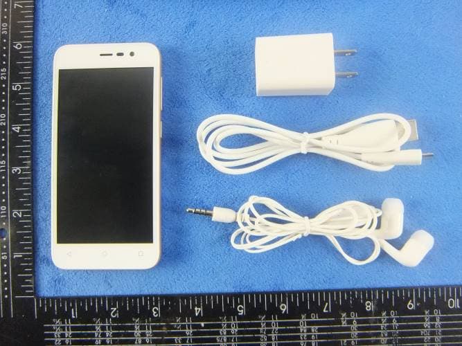
WA6S4512
Dec 23, 2015Mobile Phone
Equipment Class
DTS - Digital Transmission System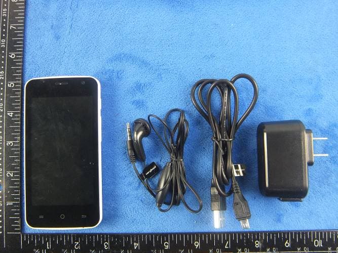
WA6SL4050
Dec 23, 2015Mobile Phone
Equipment Class
DTS - Digital Transmission System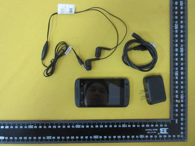
WA6S3502
Dec 07, 2015Mobile Phone
Equipment Class
DTS - Digital Transmission System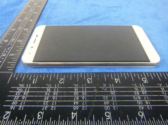
WA6SL5011
Dec 05, 2015Mobile Phone
Equipment Class
DTS - Digital Transmission System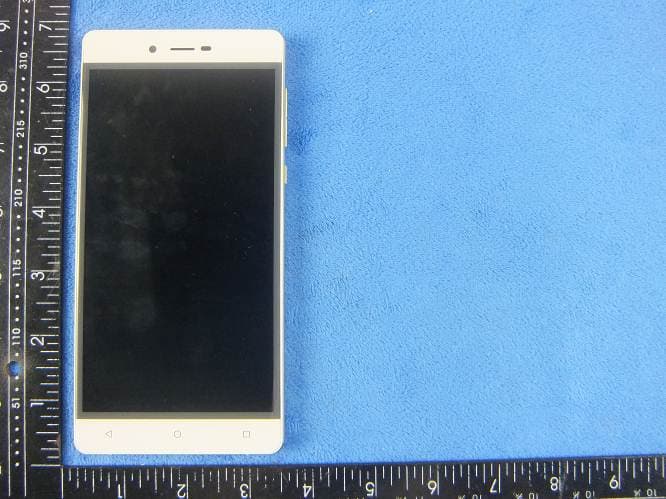
WA6SL6010
Nov 26, 2015Mobile Phone
Equipment Class
DTS - Digital Transmission System