WENCHIERDA2011UAWVHF FM Transceiver
NANAN HONGDA ELECTRONIC EQUIPMENT CO., LTD.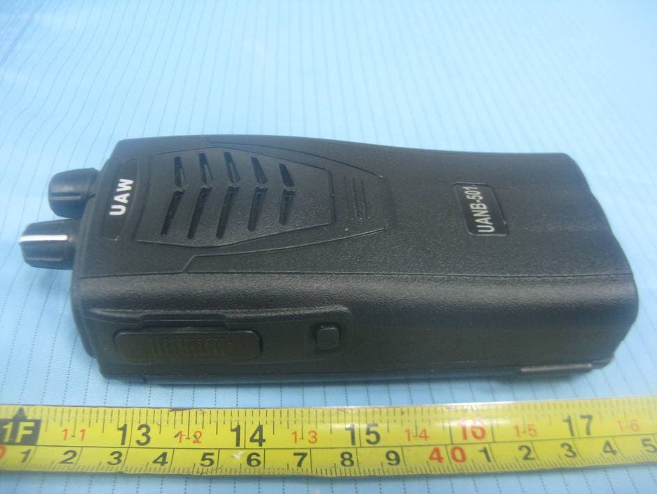
Click to zoom
Application Details
- Equipment Class
- TNF - Licensed Non-Broadcast Transmitter Held to Face
- Date of Grant
- Apr 03, 2013
- Application Purpose
- Original Equipment
- Date of Application
- Apr 03, 2013
- Equipment Note
- VHF FM Transceiver
- Frequency Range
- 136.00000000 - 174.00000000
- Country
- China
Documents & Files
Document Text
Text extracted from the exhibit documents filed with the FCC. Open a document above to read the original.
Block Diagram
1 2 3 4 5 6 78 ABCD 8 7 6 5 4 3 2 1 D CBA Title Number Revi sio n Si z e A2 Dat e: 9-Jul -2008 She et of a RXV 5V R89 VC C BATT AT24 C08 5V IC7 470 K L M2332 IC2 13M X2 PL LV LOOP FILTER CP2 1SV270 FC ONT D5 、 D6 VCO Q17 2SK508 DEVD7 1SV270 DEV PL LV Q20 2SC162 3 Q18 2SC422 6 Q21 2SC422 6 D10 D11 HSC2 77 X 2 RXV TXV Q24 2SC422 6 Q25 2SC335 7 TXV TXV Q26 2SK307 8 DRIVE AMP Q27 2SK347 6 PI NAL AMP D13 HVU131 ANT SW ANT SW ANT ENNA D12 D14 HSC2 77 X 2 ANT SW Q9 DTC114E E Q8 DTC114E E TXV TXV APC 7. 2V L M2904 APC SW IC5 Text BPF AMP BPF Q23 3SK177 RXV MI XE R Q22 3SK177 RXV MC F FL 1 、 FL 2 21. 7M IF AMP Q16 2SC418 2 RXV FL 3 450 G 31136 IC9 FL 4C24 RXV RXV Q1 DTA114E E RXV Q13 DTC114E E Q12 DTC114E E D2 GRE EN LE D D3 RED LED PL LV VCC Q32SB624 5V BUSY 32. 76 8K AUDIO 5V IC3 736 8F IC6 SW VCC VCC 21. 25 0 SP FX128E X IC10 5V MI C 455 8 IC4 TXV DEV DQT QT PT TKEY MONI KEY POWE R SW SW 2 7. 2V VCC 7. 2V 5V Q24 XC62 PF Q13 DTA114YE Q27 DTA114YE MI CV Q25BV4 TXV Q15 DTA114YE PL LV 64F2831 IC6 DTC114E E Q10 2SB624 Q11 SW16 SW 1
External Photos
EXHIBIT B - EUT EXTERNAL PHOTOGRAPHS EUT – Front View EUT – Rear View Antenna EUT – Top View EUT – Botton View EUT – Left View EUT – Right View EUT – Charger Front View EUT – Charger Rear View
ID Label/Location Info
EXHIBIT A - FCC ID LABELING AND LOCATION FCC ID Labeling Label Warning FCC ID Location The label shown shall be permanently affixed at a conspicuous location on the device and be readily visible to the user at the time purchase (Labeling requirements per 2.925) Warning location Label location
Internal Photos
EXHIBIT C - EUT INTERNAL PHOTOGRAPHS EUT – Cover off View 1 EUT – Cover off View 2 EUT – Main Board Top View EUT – Main Board Bottom View
Operational Description
1 Circuit Description RF part structure picture of model: This radio’s frequency range is 136-174MHz. In this circuit we use the project of low local oscillator. First intermediate frequency is 21.7MHz. Second intermediate frequency is 450 kHz. In the circuit we use the method of PLL so that receive/send frequency will be more stable. ANT Communal Channels RX- AMP MIXE R modu lation AF- AMP 450K TX-AMP TX-Push PLL AF-deal with Double frequenc 13MHz Speaker MIC 2 1、VCO circuit: The receiver uses the project of low local oscillator, the circuit structure as below: In this circuit, Q17 is receiving local oscillator, and also Q17 is transmitting local oscillator. Their oscillator frequencies are respectively controlled by Q17 who buildup the receiver’s voltage control circuit. And their transmitting are controlled by D5 and D6 who buildup the voltage control circuit. In the working, the circuit is on receiving or transmitting status. The signal after passed receiving/transmitting oscillator will be sent to the AMP circuit of D5 and D6 to amplify. The signal after passed D5 & D6 will be divided into 3 parts. One part will return PLL IC2 to compare and get the difference of voltage. The difference of voltage will pass the low pass circuit again to filter and control the receiving/transmitting voltage control circuit. Other two parts will be sent to receiving and transmitting AMP circuit to amplify again. PLL IC IC2 RX/TX LO Q17 Low pass VC D5 D6 AMP Q18 TX/RX AMP C P U 3 In the circuit of AF and DCS, CTCSS modulation, the tone will be sent to IC4 who buildup the tone processor. After passed the IC4, it will be sent to VCO to modulate. The DCS, CTCSS will product two part signals in IC1. One part will be sent to VCO to modulate. Other one will be sent to XC1 to modulate. 2、 The receiving circuit: In the receiving circuit, the HF signal who be received by antenna, will pass the common channel (low pass circuit), and be sent to Q23 to amplify. The signals after amplified and the signals of PLL’s local oscillator will be sent to mixer Q22 together. The signals after passed the mixer will be sent to FL1, FL2 for filtering and get the first MF 21.7MHz. The first MF signal will pass Q16 to amplify, then be sent to IC9 to mix again. The second MF 450 kHz will be produced. Modulate again will get the AF signals. The AF signals will be sent to IC1 process DCS, CTCSS and AF filter. Be sent to IC6 to amplify again. Last transmit from speaker. Mike AF process IC4 DCS、CTCSS product signal IC1 VCO AF modulation 13MHZ XC1 4 ANT T1、T2 3、 AF-AMP circuit: The signals after IC9 modulated will be sent to IC1 to process DCS, CTCSS and AF response. Then be sent to IC6 and the periphery circuit to amplify. Last push the speaker. Common channel MF filter FL1、FL2 AMP circuit Q23 MF AMP Q16 mixer Q22 Modulation circuit IC9 AF AMP IC6 21.25MHz X401 RX LO speaker AF response process IC1 AF AMP IC6 Speaker Modulation output IC9 AF Process IC1 5 4、 The transmitting circuit: The HF signals which be produced by VCO, pass the Q24, Q25 to amplify and be sent to Q26 to amplify again. Then be sent to Q27 to amplify power. The amplified power will be sent to RX/TX switch tube of D13. Last be sent to common channel and transmit out from the antenna. ANT 5、Microprocessor (MPU): The CPU system which be buildup by IC1 work on X501(32.768 kHz), and control the function of radio. First AMP Q24 Second AMP Q25 power control IC5 Push Q26 AMP Q27 Antenna switch D13 Common channel CPU IC1
Operational Description
Federal Communications CommissionDA 13-431 Before the Federal Communications Commission Washington, D.C. 20554 In the Matter of Implementation of Sections 309(j) and 337 of the Communications Act of 1934 as Amended Promotion of Spectrum Efficient Technologies on Certain Part 90 Frequencies ) ) ) ) ) ) ) WT Docket No. 99-87 RM-9332 ORDER Adopted: March 15, 2013Released: March 18, 2013 By the Chief, Wireless Telecommunications Bureau, Chief, Public Safety and Homeland Security Bureau, and Chief, Office of Engineering and Technology: 1.Introduction.In this Order, we grant in part and deny in part a Petition to Delay Indefinitely Implementation of Section 90.203(j)(5) of the Commission’s Rules filed by Ritron, Inc. (Ritron) on September 21, 2012. 1 Pursuant to Section 90.203(j)(5) of the Commission’s rules, the Commission no longer accepts applications for certification of Part 90 private land mobile radio (PLMR) equipment in the 150-174 MHz and 450-512 MHz bands that cannot operate in a 6.25 kHz mode or with equivalent efficiency. 2 Ritron requests that implementation of this requirement be delayed indefinitely. We conclude that the requirement should be waived only until January 1, 2015. 2.Background.In 1995, the Commission adopted rule changes to promote the efficient use of the PLMR service and facilitate the introduction of advanced technologies. 3 To promote the transition to a more efficient narrowband channel plan, the Commission provided, inter alia, that “only increasingly efficient equipment” would be approved. 4 The Commissiondid not set a date after which it would no longer approve equipment with a wideband (25 kHz) mode, or after which such equipment could no longer be manufactured or used. 5 The Commission contemplated that, as systems reached the end of their service life and new radios were needed, users would migrate to the narrower bandwidth multi-mode radios in order to avoid the adjacent-channel interference that could occur from systems using the adjacent narrowband channels. 6 3.Subsequently, the Commission determined that the 1995 rules failed to provide adequate incentive to realize the Commission’s spectrum efficiency goals in these bands, and stronger measures 1 SeePetition to Delay Indefinitely Implementation Section 90.203(j)(5) of the Commission’s Rules (filed Sept. 21, 2012) (Petition). 2 See47 C.F.R. § 90.203(j)(5). 3 SeeReplacement of Part 90 by Part 88 to Revise the Private Land Mobile Radio Services and Modify the Policies Governing Them, Report and Order and Further Notice of Proposed Rule Making, PR Docket No. 92-235, 10 FCC Rcd 10076, 10077 ¶ 1 (1995). 4 Id.at 10081 ¶ 7. 5 Id.at 10100 ¶ 40. 6 Id. Federal Communications CommissionDA 13-431 2 would be required to bring about a timely transition to narrowband technology. 7 The Commission therefore amended the rules to provide that, by January 1, 2013, Industrial/Business and Public Safety Radio Pool licensees in the 150-174 MHz and 421-512 MHz bands must migrate to 12.5 kHz channel bandwidth or utilize a technology that achieves equivalent efficiency. 8 4.The Commission also adopted interim deadlines to facilitate this transition to narrowband technology. Among other rules, the Commission provided that, beginning January 1, 2011, it would no longer accept applications for certification of equipment that cannot operate in 6.25 kHz mode or with equivalent efficiency. 9 In 2010, the Commission temporarily waived this requirement until January 1, 2013, 10 but stated, “If 6.25 kHz standards still are not in place at that date, interested parties may request a further extension.” 11 5.Ritron, a manufacturer of wireless products, contends that standards for 6.25 kHz technology are not yet in place and that other issues exist that justify delaying implementation of mandatory 6.25 kHz certification by manufacturers.Ritron states that no one 6.25 kHz equipment standard exists and that, in the Industrial/Business sector of the market, two incompatible and proprietary technologies have emerged. 12 Italso argues that 6.25 kHz equipment is still unduly expensive. 13 Finally, Ritron asserts that using the equipment authorization process to facilitate the transition to narrowband technology has been largely unsuccessful. 14 Itconcludes that the implementation of Section 90.203(j)(5) should be delayed until (a) a real need has been established for additional PLMR frequencies beyond those created by the transition to 12.5 kHz channels; (b) the benefits of 6.25 kHz outweigh the associated research and development, manufacturing, and product costs; and (c) a standard has emergedfor a more cost-effective voice compressor/decompressor (vocoder). 15 6.The Wireless Telecommunications Bureau, Public Safety and Homeland Security Bureau and the Office of Engineering and Technology sought comment on Ritron’s request. 16 We asked commenters to address whether the public interest would be served by further delaying implementation of 7 See Implementation of Sections 309(j) and 337 of the Communications Act of 1934 as Amended,Second Report and Order and Second Further Notice of Proposed Rulemaking, WT Docket No. 99-87, 18 FCC Rcd 3034, 3038 ¶ 12 (2003). 8 See 47 C.F.R. § 90.209(b)(5). The January 1, 2013 deadline for converting to 12.5 kHz technology has been waived for licensees in the 470-512 MHz segment of the UHF band (the T-Band). SeeImplementation of Sections 309(j) and 337 of the Communications Act of 1934 as Amended, Order, WT Docket No. 99-87, 27 FCC Rcd 4213 (T-Band Order), on recon., Order on Reconsideration, 27 FCC Rcd 14770 (WTB/PSHSB/OET 2012). 9 See Implementation of Sections 309(j) and 337 of the Communications Act of 1934 as Amended,Third Report and Order, WT Docket No. 99-87, 22 FCC Rcd 6083, 6090 ¶ 16 (2007) (Third Report and Order). 10 See Implementation of Sections 309(j) and 337 of the Communications Act of 1934 as Amended, Order, WT Docket No. 99-87, 25 FCC Rcd 8861, 8866 ¶ 11 (2010) (Order). 11 Id.at 8866 n.41. 12 …
Text truncated - open the document above for the full version.
Schematics
1 2 3 4 5 6 78 ABCD 8 7 6 5 4 3 2 1 D CBA L32 0. 4/ 1. 5/ 3T + L31 0. 4/ 1. 5/ 4T + L30 0. 4/ 1. 5/ 4T + L28 0. 4/ 1. 5/ 4T + L23 0. 4/ 1. 5/ 3T + L20 0. 4/ 1. 5/ 4T + L25 0. 4/ 1. 5/ 3T + L7 0. 4/ 1. 5/ 4T + L19 0. 4/ 1. 5/ 3T + C1775P C1781P5 C1767P C1712P C1731P C166 2P C143 0P5 C175P C172470 P C1467P C1421P C131103 P C149102 P C1741P C156 3P C1551P C16515P R1670R D14HSC2 77 CV1 3-10P CV2 3-10P Q23 3SK177 (U73) Q22 3SK177 (U73) R1401K R1161K R159100 R R160 100 K R157180 R R158220 K R13510R R114100 K R141100 R R1401K R142330 R R103 180 K R1084K7 R113100 R R1221K R104180 K R131K5 R1053K9 R1304K7 C132103 P C154102 P C89220 P C1471P C148 470 P C88220 P C90104 P C100102 P C103103 P L18 0. 4/ 1. 5/ 3T + IF-TEST R1073K3 C13015P OSCIN 1 OSCOUT 2 MIXOUT 3 VCC 4 IF IN 5 DEC 6 FIL OUT 7 FIL IN 8 AFOUT 9 QUAD 10 IFOUT 11 RSS I 12 N-DET 13 N-REC 14 GND 15 MIXIN 16 IC9 311 36 C9215P C91470 P C9582P C101102 P C97 224 P C98100 P FL 450C24 R111100 K X3 21. 25 0MHz C9968P E210u F C15104 P C95103 P C94472 P C9103 P C1 103 P R1094K7 R12522K E23 4uF7 E15 4uF7 E14100 uF R1064K7 R1100 K R541K2 C86104 P C68103 P C8102 P W110K R8110R J3 2. 5mm J2 3. 5mm R171K C69220 P SP1 SPE AKE R X1 32K768 IN 1 GND 3 OUT 2 IC8 L M2950(29 31) SW 2 C21104 P C83102 P C20104 P C13103 P C14103 P VBATT 5R C123 103 P C29103 P C76 103 P C12103 P C118103 P C117102 P C1335P R134 4K7 R124100 K R12310K R10 4K7 R1247K D9 414 8 Q2 2SB624 5C Q21 2SC422 6 C125 103 P C129 1P C122X R137 100 K Q18 2SC422 6 R132100 R C119103 P R12782K C1205P C1090P5 R29100 R Q17 2SK508 C11456P D6 1SV270 D5 1SV270 C104103 P C113 103 P D7 1S V 270 R2847K R119100 K R2922K R13110R R325K6 C108 470 P C31 103 P C1122P RV350K E12 10u F D8HSC2 77 Q19 DTC144E E R1293K3 C115102 P C77102 P VCC1 1 VP1 2 Do RF 3 GDN 4 RFIN 5 -RFIN 6 GND 7 OSCIN 8 GDN 9 FoL D 10 CLOCK 11 DAT A 12 LE 13 GND 14 -FIN IF 15 FI N I F 16 GND 17 Do IF 18 VP2 19 VCC2 20 IC2 L M2332 R310R R610K C22 100 P C23100 P C24100 P C27 100 P C30103 P C28102 P R117 560 R R118560 R R1204K7 R121 4K7 E220uF1 E211uF R241K R58 120 K R10010K R21 47K C51103 P D1 414 8 D13HVU131R75270 R R720R39 R730R39 R710R39 R16247K R1660R R16147K R15347R R16447R C153102 P C145102 P C161470 P C15227P C151102 P C150470 P C163104 P C162103 P C159 2P C169 7P C16020P C170 100 P C137470 P R156120 K R150 1K5 R15547K R14647K R14822R R1433K3 R1443K3 R6347K R149680 R Q27 2SK347 6 Q26 2SK307 8 Q25 2SC335 7 Q24 2SC422 6 Z1 USB Z2 USB C52102 P C141470 P C56 102 P C136470 P R1520R C60 102 P C59 470 P D11 HSC277 R6210K R591M C54470 P 7 + 5 - 6 IC5 L M2904 E11 4uF7 1 + 3 - 2 84 IC5 290 4 Q9 DTC114E E R60220 K R5768K R5647K R6410K R69150 K R68150 K R70150 K VB+ VB+ R66150 K R61150 K R67150 K VBATT Q8DTC114E E R93330 R C165104 P C164470 P C7 102 P R12210K TPD MK1 MI C R38 33K C34103 P C135470 P 1 + 3 - 2 84 IC4455 8 7 + 5 - 6 IC4455 8 C47223 P C48273 P C50470 P C43223 P R47680 K R4818K R49100 K R511K8 C46102 P C49104 P R4333K R52470 R R423K3 R441K5 R40 6K8 R5030K R4622K 5V E84uF7 C42 100 P C41470 P C35332 P C44470 P E1010u F ANT 1 C2100 P 5V KEY PT T MONIKEY D3RED 5T C57103 Q11 2SB624 R7847K E13 10u F C67104 P C66 102 P VBATT 1 C64102 P R791K8 Q10 DTC144E E C55 470 P Q6 2SC418 1 R451K E92uF2 C45104 P L51UH L132R2J L1218NH L1118NH L10 100 NH L827NH L7120 NH L66uH8 L9100 NH L211uHL24100 NH L27100 NH L22 2NH2 L17 18NH L1518NH C1107P C1115P C1791P C1751P5 D12HSC2 77 C571P R1630R R151 10R C13910P R13910K D10HSC2 27 C128 6P R147330 R L16100 NH L4100 NH C1214P C26 4P C116 103 P R12810K 5C C79102 P RV2 50K R1933K R9422K R87100 K E16 4uF7 5R 5C L2100 NH R83470 R D2 GRE EN R82470 R R3910K C40473 P C1915P C1815P 5V A0 1 A2 2 A3 3 GND 4 SDA 5 SC L 6 WP 7 VCC 8 IC7 AT24 C08 R98 47K R10247K R1582K R101 47K R99 47K 5V R14100 K R5 10K R16 15K R110 220 R C75 102 P R4 47K R9368K R55100 R Q13 DTC114E E Q12 DTC114E E VBATT 1 5T C16 103 P C138 470 P R74270 R L29220 NH C168 X R115220 K R7 10K R2747K R26100 K R25100 R E20 10u F C11102 P R76150 R C53 104 P R1453K3 R136270 R C126470 P 5V Q3 2SB624 VBATT 1 R88150 K(F) R89 470 K(F) C74103 P R22 27K R846K8 R864K7 R854K7 C72273 P C71273 P C58470 P C81103 P R9647K 5V FUN1KEY C80103 P R9547K R7710K C78470 P R90 1K R802K2 R3147K R23150 K E110u F C37X C65124 P R2390 K CTCSS OUT DCS OUT E61uF C107 104 P L3 6uH8 5R L14 18N H FL 1 21. 7MHz FL 3 450 E FL 2 21. 7MHz Q1 DTA114E E Q14 DTA114E E VBATT 1 Q16 2SC418 2 Q20 2S C1 623 Q7 1SS372 SQL-A D RX-P RX-P RXI RXO RXI RXO PF1SC K2 4SDAAUBEEPTX-PCODE4CODE3CODE2CODE1 SQL-AD RXLEDTXLED TXLED RXLED P O W736 8 PTT/RXD PF2 HI/LO TXD LDPLL LEPLL SDA24 SCKPLL DCS OUT MCU5V GND5VSC K2 4SDA2 4 C87 103 P C85 103 P C84 103 P C82 103 P VR 1 GND 2 fout 3 Vcc 4 X2 13. 0MHz L26 0. 31/ 1. 0/ 10 T+ 1234 5 SW 1SW 16 HI/ L O Q4 2SC461 7 Q5 2SC461 7 R3433K C33 680 P C38332 P R361M8 R33 10K C73220 P C32472 P R351M8 R3733K C39473 P C36680 P R41 33K 5T E72uF2 LDPLL LEPLLSDA2 4 SC KP LL CTCSS OUTMI C AMP1 R2233K RV1X MI C AMP1 5C1 MI C AMP MIC AMP TX/RX VCO 12345 678910 IC6 736 8F C62103 P 1234 5678 IC3 AUDIO 5V C10104 P R91K R847K SDAAU SCK24 AUDIO AUDIO C63100 P C70474 P C61102 P BEEP AFO IN TXD PF2PF1 PT T/ R XDPOW73 68 CODE4CODE3CODE2CODE1 SQL-AD C134 5P E510u F R20180 R C25223 P C105 2P C106 0P5 C124 X E1922u F E1822u F R303K3 C158 X R133 0R C1273P C102104 P C93102 P R53100 R R65 X 5C R1147K F1 FUSE L1 60T (2A ) C5102 P C6 103 P D4 1S R1 54-400 C3103 P C4104 P E310u F R1380R C181 X 5V E4 10u F TX-P E17 10u F R91 47K 5C1 5C1 C1407P R167 10K R9710K C180 X Q15 DTA114E E 1 1 2 2 3 3 4 4 5 5 6 6 7 7 8 8 9 9 10 10 11 11 12 12 13 13 14 14 15 15 16 16 17 17 18 18 19 19 20 20 21 21 22 22 23 23 24 24 25 25 26 26 27 27 28 28 29 29 30 30 31 31 32 32 33 33 34 34 35 35 36 36 37 37 38 38 39 39 40 40 41 41 42 42 43 43 44 44 IC1 MC U44 R500100 K R5011K VOX-DE C VOX-DEC 5T C501104 P R503100 K C502100 P R5021K C503104 P R505220 K Q281SS372 PI N15PI N16 GND GND 1 1 2 2 3 3 4 4 5 5 6 6 7 7 8 8 9 9 10 10 11 11 12 12 13 13 14 14 15 15 16 16 IC10 FX128E 4 No Sc r a m bl e No Sc r a m bl e R440100 K R3300R R442100 K R4431M R441100 K …
Text truncated - open the document above for the full version.
Test Report
Note: This test report is prepared for the customer shown above and for the equipment described herein. It may not be duplicated or used in part without prior written consent from Bay Area Compliance Laboratories Corp. This report must not be used by the customer to claim product certification, approval, or endorsement by NVLAP*, NIST, or any agency of the Federal Government. * This report may contain data that are not covered by the NVLAP accreditation and shall be marked with an asterisk“★” FCC PART 90 TEST REPORT For NANAN HONGDA ELECTRONIC EQUIPMENT CO., LTD. Zian Road, Jiangnan High-Tech Industrial zone, Quanzhou, China FCC ID: WENCHIERDA2011UAW Report Type: Original Report Product Type: TRANSCEIVER Test Engineer: Eric Lee Report Number: RXM11051051-00 Report Date: 2012-11-30 Reviewed By: Alvin Huang RF Leader Test Laboratory: Bay Area Compliance Laboratories Corp. (Shenzhen) 6/F, the 3rd Phase of WanLi Industrial Building ShiHua Road, FuTian Free Trade Zone Shenzhen, Guangdong, China Tel: +86-755-33320018 Fax: +86-755-33320008 www.baclcorp.com.cn Bay Area Compliance Laboratories Corp. (Shenzhen) Report No.: RXM11051051-00 FCC Part 90 Page 2 of 29 TABLE OF CONTENTS GENERAL INFORMATION.......................................................................................................................................4 PRODUCT DESCRIPTION FOR EQUIPMENT UNDER TEST (EUT) .....................................................................................4 OBJECTIVE...................................................................................................................................................................4 RELATED SUBMITTAL(S)/GRANT(S).............................................................................................................................4 TEST METHODOLOGY..................................................................................................................................................4 TEST FACILITY.............................................................................................................................................................4 SYSTEM TEST CONFIGURATION ..........................................................................................................................6 DESCRIPTION OF TEST CONFIGURATION......................................................................................................................6 EQUIPMENT MODIFICATIONS.......................................................................................................................................6 CONFIGURATION OF TEST SETUP.................................................................................................................................6 BLOCK DIAGRAM OF TEST SETUP................................................................................................................................6 SUMMARY OF TEST RESULTS...............................................................................................................................7 FCC §1.1307(b) & §2.1093 - RF EXPOSURE.............................................................................................................8 APPLICABLE STANDARD..............................................................................................................................................8 FCC §2.1046 & §90.205- RF OUTPUT POWER........................................................................................................9 APPLICABLE STANDARD..............................................................................................................................................9 TEST PROCEDURE........................................................................................................................................................9 TEST EQUIPMENT LIST AND DETAILS...........................................................................................................................9 TEST DATA................................................................................................................................................................10 FCC §2.1047 & §90.207 - MODULATION CHARACTERISTIC ..........................................................................11 APPLICABLE STANDARD............................................................................................................................................11 TEST PROCEDURE......................................................................................................................................................11 TEST EQUIPMENT LIST AND DETAILS.........................................................................................................................11 TEST DATA................................................................................................................................................................11 FCC §2.1049, §90.209 & §90.210 – OCCUPIED BANDWIDTH & EMISSION MASK......................................17 APPLICABLE STANDARD............................................................................................................................................17 TEST PROCEDURE......................................................................................................................................................17 TEST EQUIPMENT LIST AND DETAILS.........................................................................................................................17 TEST DATA................................................................................................................................................................18 FCC §2.1051 & §90.210 - SPURIOUS EMISSIONS AT ANTENNA TERMINALS ............................................20 APPLICABLE STANDARD.................................................................................................................................…
Text truncated - open the document above for the full version.
Contact Information
Applicant
Dalen Bao(Export Manager)
Test Firm
Bay Area Compliance Laboratory Corp. (Shenzhen)John Chan
Technical Specifications
| # | Rule Parts | Frequency Range | Power Output | Emission | Tolerance |
|---|---|---|---|---|---|
| 1 | 90 | 136 MHz - 174 MHz | 4.99 W | 8K10F3E | 1.2300000000 ppm |
Other Applications from NANAN HONGDA ELECTRONIC EQUIPMENT CO., LTD.

WEN-DUA1000
Jun 02, 2015Digital Two-Way Radio
Equipment Class
TNF - Licensed Non-Broadcast Transmitter Held to Face