X7F-DK-EM4PSAUTO INTEGRATED DIALING TEST TERMINAL
NINGBO PUTIAN COMMUNICATION TECHNOLOGY CO., LTD.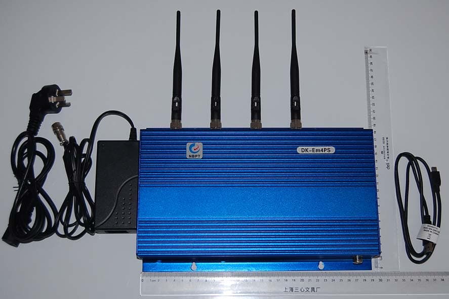
Click to zoom
Application Details
- Equipment Class
- PCB - PCS Licensed Transmitter
- Date of Grant
- Apr 11, 2010
- Application Purpose
- Original Equipment
- Date of Application
- Apr 11, 2010
- Equipment Note
- AUTO INTEGRATED DIALING TEST TERMINAL
- Frequency Range
- 1850.20000000 - 1909.80000000
- Country
- China
Documents & Files
Document Text
Text extracted from the exhibit documents filed with the FCC. Open a document above to read the original.
Users Manual
Ningbo Putian Communication Technology Co., Ltd DK-Em4PS Instruction for D K - E m 4 P S Auto-dial testing Device - 1 - Ningbo Putian Communication Technology Co., Ltd Ningbo Putian Communication Technology Co., Ltd Table of Contents 1、OVERVIEW.......................................................................................................................... 3 2、PERFORMANCE AND CHARACTERISTICS FOR PRODUCTS....................................... 4 2.1. BASIC FUNCTIONS AND FEATURES........................................................................... 4 2.2. OPERATION MODE FOR COMMUNICATION.............................................................. 4 3、PERFORMANCE INDICATORS FOR ALL KINDS OF CHANNEL.................................... 5 4、PERFORMANCE INDICATORS FOR DEVICE................................................................... 6 5、DESCRIPTION FOR DK-EM4PS INSTALLATION............................................................. 7 5.1. ANTENNA INSTALLATION............................................................................................. 7 5.2. POWER CONNECTION................................................................................................. 7 5.3. USB CABLE CONNECTION........................................................................................... 8 5.4. NETWORKING............................................................................................................... 9 5.5. INDICATOR DESCRIPTION........................................................................................... 9 5.6. CASE SIZE..................................................................................................................... 9 6、INSTRUCTION FOR DK-EM4PS DEVICE........................................................................ 10 6.1. DESCRIPTION FOR SIM CARD INSTALLATION........................................................ 10 6.2. DESCRIPTION FOR APPLICATION PROGRAM INSTALLATION.............................. 14 6.4. DESCRIPTION FOR APPLICATION PROGRAM'S USE............................................. 18 6.5. NOTES.......................................................................................................................... 20 7、FCC STATEMENT............................................................................................................. 21 - 2 - Ningbo Putian Communication Technology Co., Ltd 1、Overview D K - E m 4 P S Auto-dial testing Device is a Wireless Test Product based on Mobile communication network platform, this product is tested up to 4 channels embedded。Test channel can be configured according to test requirements. including 2 channels for GSM and 2 channels for TD-SCDMA. The device adopts standard design of industrial-grade, with English and Chinese SMS sending, voice and wireless data mode functions and etc. Users can connect with PC by USB2.0 port & Ethernet Interface。This device can be widely used in monitoring for mobile network coverage。 - 3 - Ningbo Putian Communication Technology Co., Ltd 2、Performance and Characteristics for products 2.1. Basic functions and features 2.1.1. Extend up to 4 test channels, reality a multi-channel for voice, data, wireless transmission function between different Signal System mobiles。 2.1.2. Testing Communication & test channel for 4 channels can be configured according to any requirement。 2.1.3.Support GSM Module, can be Transmit with 4 different Signal System channel,。 2.1.4. ARM11 Processor Embedded can carry on management of multi-channels & Switching Control; 2.2. Operation mode for Communication 2.2.1.USB port: This port can carry out High-Speed Communication between local computers, data dial, voice, SMS functions and etc. 2.2.2. Ethernet Interface: this interface supply connection between device and computers, is used for Configuration of device parameters and functions, it is easy to maintenance device。 - 4 - Ningbo Putian Communication Technology Co., Ltd 3、Performance Indicators for all kinds of channel Performance Indicators for GSM channel Module Basic characteristics Description remark Signal System GSM Default Configuration Frequency band 850/900/1800/1900MHz Transmit Power Class 4 (+33dBm ± 2dB) for EGSM850 Class 4 (+33dBm ± 2dB) for EGSM900 Class 1 (+30dBm ± 2dB) for GSM1800 Class 1 (+30dBm ± 2dB) for GSM1900 Class E2 (+27dBm ±3dB) for GSM 850 8-PSK Class E2 (+27dBm ±3dB) for GSM 900 8-PSK Class E2 (+26dBm +3 /-4dB) for GSM 1800 8-PSK Class E2 (+26dBm +3 /-4dB) for GSM 1900 8-PSK Data Transmission GPRS: Multislot Class 12 Full PBCCH support Mobile Station Class B Coding Scheme 1-4 EGPRS: Multislot Class 10 Mobile Station Class B Modulation and Coding Scheme MCS 1-9 CSD: V.110, RLP, non-transparent 2.4, 4.8, 9.6, 14.4kbps USSD: PPP-stack for GPRS data transfer SMS MT, MO, CB, Text and PDU mod SMS storage: SIM card Support transmission of SMS alter User can choose preferred mode. SIM card Supported SIM card: 1.8V ,3V External antenna Connected via 50 Ohm antenna connector or antenna pad - 5 - Ningbo Putian Communication Technology Co., Ltd 4、Performance Indicators for device Type DK-Em4PS Power Supply of Module (10~30)V DC Power Supply (85~264)V AC 50/60Hz (Adapter) Grounding earthing of casing System power <20W Case Size 290mm*190mm*45mm Case design Vibration、Drop resistance 、Waterproof Specifications Mean Time Between Failure ≥10000 hours Others Work Temperature ≥-10°C,≤+55°C Storage temperature ≥-20°C,≤+65°C Normal humidity ≤95% Work atmosphere ≥62 kPa,≤106kPa - 6 - Ningbo Putian Communication Technology Co., Ltd 5、Description for DK-Em4PS Installation 5.1. Antenna Installation There are 4 SMA ports at the top of a device; users install Antenna with different Module Configurations according to channels and 1-4 Numerical order on it。As shown in Figure 5-1-1: Figure 5-1-1 Location of Antenna installation Note:The antenna must be installed before a device switched on! Otherwise, the module may be damaged! 5.2. Power Connection Insert an …
Text truncated - open the document above for the full version.
Block Diagram
Block Diagram 824 – 849MHz 1850–1910MHz
Cover Letter(s)
深圳市华标电子科技有限公司 Bontek Compliance Testing Laboratory Ltd 深圳市南山区侨城东路华侨城东部工业区东H-3栋1楼 1/F, Block East H-3, OCT Eastern Ind. Zone, Qiaocheng East Road, Nanshan, Shenzhen, China Tel: +86-755-86337020 Fax: +86-755-86337028 Http:/ / www.bontek.com.cn DATE: February 19, 2010. Dear TCB Section of Timco Engineering, Inc., Thank you for cooperation. I would like to submit FCC application of Ningbo Putian Communication Technology Co., Ltd. /FCC ID: X7F-DK-EM4PS by your TCB Approval today. Best Regards, Bontek compliance Testing Laboratory Ltd. Tony Wu General Manager
Cover Letter(s)
Cellstar I.L Ltd FCC ID:X7F-DK-EM4PS POWER OF ATTORNEY February 13,2010 Federal Communications Commission Authorization and Evaluation Division 7435 Oakland Mills Road Columbia, MD 21046 To Whom It May Concern: We, the undersigned, hereby authorize Bontek Compliance Testing Laboratory Ltd. (Tony Wu) on our behalf, to apply to the Federal Communications Commission on our equipment. Any and all acts carried out by Bontek Compliance Testing Laboratory Ltd. (Tony Wu) on our behalf shall have the same effect as acts of our own. This authorization expires on March 10, 2010. This is to advise that we are in full compliance with the Anti-Drug Abuse Act. We, Ningbo Putian Communication Technology Co., Ltd. are not subject to a denial of federal benefits pursuantto Section 5301 of the Anti-Drug Act of 1988, 21 USC853a, and no party to the application is subject to a denial of federal benefits pursuant to that section. Sincerely, Ningbo Putian Communication Technology Co., Ltd. ------------------------------- Mao Lei Deputy Chief Engineer
External Photos
TCF No.: BCT09LR-1303 DK-Em4 External photos EUT-Top View EUT-Bottom View EUT-Front View EUT-Back View EUT-Right View EUT-Left View
ID Label/Location Info
TCF No.: BCT09LR-1303 CE Label Location
Internal Photos
TCF No.: BCT09LR-1303 DK-Em4 Internal Photos Full View Mainboard To p Vi e w Bottom View Core To p Vi e w Bottom View Channelboard To p Vi e w Bottom View SIMboard To p Vi e w Bottom View
Operational Description
TCF No.: BCT09LR-1303 Adjustment Instruction for GSM Channel Basic characteristics Description Remark Signal System GSM Default Configuration Frequency band 850/900/1800/1900MHz Transmit Power Class 4 (+33dBm ± 2dB) for EGSM850 Class 4 (+33dBm ± 2dB) for EGSM900 Class 1 (+30dBm ± 2dB) for GSM1800 Class 1 (+30dBm ± 2dB) for GSM1900 Class E2 (+27dBm ±3dB) for GSM 850 8-PSK Class E2 (+27dBm ±3dB) for GSM 900 8-PSK Class E2 (+26dBm +3 /-4dB) for GSM 1800 8-PSK Class E2 (+26dBm +3 /-4dB) for GSM 1900 8-PSK Data Transmission GPRS: Multislot Class 12 Full PBCCH support Mobile Station Class B Coding Scheme 1-4 EGPRS: Multislot Class 10 Mobile Station Class B Modulation and Coding Scheme MCS 1-9 CSD: V.110, RLP, non-transparent 2.4, 4.8, 9.6, 14.4kbps USSD: PPP-stack for GPRS data transfer SMS MT, MO, CB, Text and PDU mod SMS storage: SIM card Support transmission of SMS alter User can choose preferred mode. SIM card Supported SIM card: 1.8V ,3V External antenna Connected via 50 Ohm antenna connector or antenna pad
Operational Description
TQX-900/1800BF WIRELESS ANTENNA TQX-900/1800BF Antennas for Wireless Public Telephone, which Our Company makes useful of specialized analysis software for advanced wireless antenna to produce after optimizing design, specifically developed a series of wireless public telephone antennas for Frequency Range 900/1800 MHz。Its characteristics is with a band working frequency, strong anti-interference, simple structure, robust, easy installation。 All Antennas is tested by HP network analyzer from the United States before delivery。 Specifications Type TQX-900/1800BF Frequency Range-MHz A:885~960 B:1710~1880 Bandwidth-MHz A:70 B:170 Gain-dBi 2.0 VSWR A:≤2.0 B:≤2.5 Input Impedance-Ω 50 Polarization Vertical Maximum Power-W 25 Connector Type SMA 头(加长) SMA head (collapsible) Antenna size-mm 长 100 Long 100 Weight-g 30
Operational Description
Principle & block diagram for DK-Em4PS Auto-dial testing Device Overview DK-Em4PS Auto-dial testing Device is a Wireless Test Product based on Mobile communication network platform, this product is tested up to 4 channels embedded。Test channel can be configured according to test requirements. including 2 channels for GSM and 2 channels for TD-SCDMA. The device adopts standard design of industrial-grade, with English and Chinese SMS sending, voice and wireless data mode functions and etc. Users can connect with PC by USB2.0 port & Ethernet Interface。This device can be widely used in monitoring for mobile network coverage。 Principle of DK-Em4PS is shown in figure 1 Figure1 Block Diagram for the Principle of DK-Em4 As shown in figure 1, DK-Em4PS device is made of three parts, namely backplane, channel plate and core plate。The core board makes use of ARM11 core processors, mainly for data transmission and processing, through the network chip DM9000A to achieve connection with Internet。 The core board reality the data communication and function control with the channel plate through USB port and serial interface. DK-Em4PS device supports up to four channels test at the same time。 The backplane is the bridge connecting a core board and a channel plate, through the USB-HUB and STM32 processors on the floor plate, to achieve data transmission channel plate and signal control。The main interfaces on the backplane are: 1. Ethernet Interface: Network chip DM9000A 2. USB-OTG port: Upgrade the inner core of a core board 3.USB-host Port: Convert 4 USB ports through USB-HUB clips on the backplane to use for communication with channel plate。 4. RS232 port: connected with COM0 at the core plate to use for communication with LINUX Console。 5. SIM card port: total 4, corresponding to 4 communication modules 6. Audio Interface: AC97 audio chip。 7. Power Interface: Input voltage 12VDC (220VAC input needs be converted by an adapter) 8. Antenna Interface: Used for Coupling between Communication module signal and spatial signal。 Channel plate is mainly used for completion of a test function, the diagram block for the Principle of a channel plate shown in Figure 2。 824 – 849MHz 1850–1910MH Figure 2 Diagram for the Principle of a channel plate The channel plate is made of 3 parts, namely Power management part, communication module part and the DTMF detection part。 Power management part of them is mainly used for the module power control。 Communication module part is made of the USB and AUDIO signals mainly, USB is used for a communication module and a core board, AUDIO signal is used for Voice record & play of the module ‘sound。 DTMF detect is mainly used for detecting DTMF code。 SIM port: used for connecting between port & outer SIM card。 The principle of the module is shown in Figure 3: Figure 3 Module Block Diagram As shown, the module function can be divided into the following functional components: Baseband Module TD-SCDMA Modem Module TD-SCDMA RF Module GPRS/EDGE RF Module RF Front End Module
Parts List/Tune Up Info
Ningbo Putian Communication Technology Co., Ltd Device's name Products List NameSpecificationAmount Remark BottomDK-Em41 Core Board6410 core board1 channel board Em4 channel board 4 BoxDK-Em4 box1 Triangle screwEm4 Screw12 Module Feederfeeder4 Air PlugAir plug1 Adapter for power 220VAC convert 12VDC 1 AntennaTQX-900/1800BF4 Module communication module 4 Ningbo Putian Communication Technology Co., Ltd PCB Name ARM 4-channel circuit backplane PCB REV DK-EM4-MAINBOARD-S V1.2 09-11-30 Document No. Production date: applied BatchAmount Developed:checked:Approval: Name Specificatio n PackageAmountBit No.Remark Capacitor15PF06032C38 C42 Capacitor22PF06036C10 C14 C44 C46 C15 C17 Capacitor220P06035C59 C61 C87 C97 C98 Capacitor104060355 C7 C11 C13 C16 C18 C19 C21- C23 C26-C35 C37 C39-C41 C43 C47-C54 C56-C58 C64 C66-C69 C71 C72 C74 C76 C79 C82-C84 C86 C89 C90 C92-C94 C96 Capacitor10408055C25 C99 C108 C125 C127 Capacitor105060314 C2 C4 C5 C12 C36 C63 C65 C70 C73 C75 C77 C78 C91 C95 Capacitor4750603C80 C81 C85 C88 Tantalum Capacitor 10uF/16V352812 C1 C6 C8 C9 C20 C24 C55 C100 C107 C109 C110 C126 Tantalum Capacitor 22uF/6.3V32163C3 C60 C62 Nickel capacitor 10uF/35V12104C101-C104 使用10uF/16V钽 电容代替 Tantalum capacitors instead of using the 10uF/16V Chip Capacitor470uF/16VC_SMT3C105 C106 C111 Capacitor103/2KVRAD0-31C45 Capacitor006031R98 Capacitor2206037R17 R18 R66-R68 R69 R70 R15, R22 not welding Capacitor49.9 1%06034R29-R32 Capacitor68006038R14 R33 R40 R42-R45 R82 Capacitor2K06031R12 Capacitor2.43K06031R35 Capacitor4.7K06038R71 R72 R74-R77 R79 R80 Capacitor6.8K08051R41 Capacitor8.2K06034R73 R78 R81 R83 Capacitor10K060337 R7-R11 R28 R34 R36-R39 R46- R57 R87-R95 R97 R102-R105 Capacitor15K060310R13 R16 R19-R21 R23-R27 Capacitor47K06035R58 R59 R84-R86 Capacitor100K06037R1 R60-R65 BeadsINDUCTOR12063L1-L3 Inductance33uHL3_SMT1L4 Transistor2N5551SOT-238Q1-Q8 Light-emitting diode GLEDLED5D1-D5 5-line LED diode1N4148MLL-342D6 D9 Schottky DiodeSS33SMC-12D7 D8 Single-row 3- pin pin CON3SIP32J24 J25 General, 2.54 Pitch Double-row 50- pin SMT Female CONN SOCKET 25x2 idc50_sm t 6J1 J2 J6-J9 Double-row 10- pin SMT Female CON_POWER idc10_sm t 8J10-J17 SIM card socket (pop-up) CON8SIM_84J18 J19 J27 J28 pin single row socket CON6SIP62J20 J21 General, 2.54 Pitch pin single row socket CON6SIP62J3 J26 General, 2.55 Pitch Double-row 20- pin pin CON20IDC201J29 General, 2.56 Pitch XH-2 power outlet CON2XH21J23 Single-row two- pin pin CON-2sip21J22 Bending-pin DB9 socket, female head DB9DB9-F1P1 Transformer RJ45 head with a network ETH_CONRJ45-31J5 Double-row 10- pin pin CON10IDC101J4 Double row of 100-pin Chip Female CON100 idc100_s mt 2U1 U2 mini USBoutletUSB-MINIUSB-MB1CN1 STM chipSTM32F103VCtqfp1001U4 Network chipDM9000ALQFP481U5 max232 chipMAX232so-161U7 USB4-port HUB- chip UPD720114TQFP481U6 Button Battery socket CR1220BAT11BAT1 电源芯片Power Chip LM2596 TO-220- 52 1U16贴片SMD 电源芯片Power Chip MAX682so-81U3 Power ChipSPX1587TO-2631U17 Power ChipAMS1117-1.8SOT2231U22 Electronic Switch SGM3005 SOP10- 20-118 7U8-U13 U15 Voice ChipWM9713LQFN481U14 Crystal32.768Kyj261X1 Crystal8M49S1X2 Crystal30M49S1X3 Crystal25.000M49S1X4 Crystal24.576Mho-361X5 Ningbo Putian Communication Technology Co., Ltd PCB Name EM4-CHBOARD PCB REV EM4-TD6311 V10 2009.10.15 Document No. Production date:applied BatchAmount Developed:checked:Approval: Name Specificatio n PackageAmountBit No.Remark Resistance100K06032R6 R7 Resistance10K06032R8 R28 Resistance24K06031R27 Resistance2K06033R31 R30 R55 Resistance4.7K06031R48 Resistance006033R39 R40 R41 Resistance300K06031R5 Capacitor10U/16V352813 C4 C12 C11 C10 C9 C22 C21 C20 C19 C18 C17 C16 C15 Capacitor10406034C1 C34 C23 C8 Capacitor10P06031C35 Capacitor20P06032C2 C3 Capacitor30P06031C36 Crystal3.5795MXTAL11Y2 293021U5 HT9170SOL-181U4 SMG3005MSOP101U6 50-pin pin1J3 10-pin pin2J1,J2 ModuleTD63111 Ningbo Putian Communication Technology Co., Ltd PCB Name 6410 core board PCB REV CORE Document No. Production date::applied BatchAmount Developed:checked:Approval: NameSpecificationPackageAmounBit No.Remark Capacitor10PF06032C1,C5 Capacitor15PF06032C46,C51 Capacitor22PF06032C43,C47 Capacitor33PF06032C2,C3 Capacitor10206032C13,C14 Capacitor107321637 C7,C8,C9,C11,C12,C15,C 19,C21,C22,C29,C31,C32 ,C34,C37,C41,C42,C44,C 48,C49,C52,C53,C54,C55 ,C56,C66,C92,C120,C121 ,C122,C124,C125,C126,C 127,C129,C131,C132,C13 4 ,C136,C137 Capacitor104040225 C57,C60,C85,C86,C145,C 147 C10,C16,C17,C20,C23,C2 8,C30,C33,C35,C36,C39, C61,C68,C69,C70,C87,C1 48 C63 C64 C71 Capacitor10504022C18,C45 Capacitor47504022C4,C6 Resistance0040213 R1,R2,R5,R6,R10,R16,R1 7,R59,R60,R61,R76,R78, Resistance22040211 R26,R27,R28,R32,R33,R5 5,R56,R114,R115,R118,R 119,R127 Resistance49.904024R31,R34,R35,R36 Resistance10004022R43,R44,R126 Resistance47004021R75 Resistance68004027 R29,R37,R62,R65,R66,R6 7,R68 Resistance1.5K04022R57,R90 Resistance2K04022R41,R42 Resistance2.43K04021R94 Resistance4.7K04027 R15,R20,R38,R46,R52,R5 3,R54 Resistance6.8K04021R30 Resistance8.2K04021R230 Resistance10K040214 R70,R71,R106,R107,R108 ,R109,R110,R111,R112,R 113,R116,R117,R120,R12 Resistance100K04023 1 R64,R80,R82 Resistance150K04021R229 Resistance330K04021R58 Inductance4.7uH50503LA3 LA4 LA5 LA6 Single-row 3-pin pin CON3SIP31J4 Thin-switchCON12SSOP121CAT1 RESET ButtonRESETRESET1SW1 BeadINDUCTOR08053L1,L2,L3 Diode1N4148MLL-341D2 Light- emitting diode GLED0805LED1D1 Double-row 50-pin pin CONN SOCKET 25x2 idc50_12 7 2J1 J51.27 Double-row 100-pin socket CON100 idc100_1 27 2J2 J31.27 Treatment Chip S3C6410XH-66FBGA4241U5 Flash chipK9K8G08U0MWSOP481U8 clipK4X51163PGFBGA602U3 U4 Power ChipXC9216A12CMRDBV51U8 Power ChipXC9216A18CMRDBV52U10 U11 Power ChipXC9216A11CMRDBV51U7 Power ChipXC6219B331MRDBV52U1 U2 Reset ChipMAX811-TDBV41U9 Crystal12Mso-361Y1 Crystal27Mso-361Y2 Crystal32.768k49S1Y3 Crystal48Mso-36-21Y4
Schematics
L4 C106 C81 C82 J21 C80 C83 U16 C105 R77 R72 R76 R71 D7 C111 D8 C104C102 C103C101 J28 J26 J27 J3 VCUT C97 R8 R93 R63 R64 R65 C67 C74C75 C68 C90 C91 C92 R58 C98 U15 J8 C51 U10 U13 J12 X5 C58 FM4 FM2 J17 CHBOARD4 R26 R27 R94 FM5 C109 FM3 J9 U11 J13 R85 R89 C107 C110 C99 C100 C127 C126 R88R86 C52 J25 R87R84 J22 U22 CH2_SIM J19 C88 C89 R75 R80 CH1_SIM J18 C85 R74 C86 R79 J24 C108 U17 C125 J20 J23 U2 C22 U4 C18 R10 X2 C14 X1 J16 C10 J2 C6 C9 Q5 Q6 Q7 C7 C11 R7 C15 C17 C13 R9 D6D9 C71C73 C76 R59 C84 C96 C69 R78 R83 R49 R57 R51 R52 R54 Q8 CHBOARD3 BAT1 C63 C64 C70C72C77 C78 C61 C79 L3 C60 C62 C87 R73 R81 R23 R25 R53 R60 R61 R62 C65 C66 U14 C93 C94 C95 R82 C59 R37 J14 C43 C38 U6 C26 C40 X3 C39 C42 R13C27 C32 R35 R24C41 R19 CHBOARD1 C8 L2 C31 R16 R91 U8 U1 C1 J1 J6 C49 J10 R90 J15 C55 R68 R69 R70 C2 R67 R66 R21 R92 R48 R50 R46 R47 CHBOARD2 R18R15R17R22 R20 R56 Q3 Q4 Q2 C16 R55 Q1 C25 C24 L1 J7 C50 U9 C23 R11 J11 U12 C57 D5 D4 D3 D2 D1 FM1 J5 CN1 P1 R45 R44R43 R42 R40 C4 C56 C48C53 R103R104R105R95 R97 R98 R102 R14 C45 C33 R29C21 C20 R30R31 R32 C34R33 C3 U3 U7 C54 GND C37 C35 R41 R1 C5 C47 PA10 PA9VCC BOOT0 1 J4 JTRST JTDIJTMSJTDOJTCK J29 R12 C44 C29 NRESET C12 C30 U5 C46 C19 X4 R34R36R38C28R39 C36 ------------------------- Date: [2009, 8, 11, 3] Designer: Administrator Title: PT_D380_P2 Drawing No:______________ ------------------------- X3001 U6003 U3001 U2001 U1001 T5002 T5001 T8013T8012T8008T8005T8004T8003T8002T1004T1002 R8008 R8007 R5008 R5007 R5012R5011 R3002R1025R1023 R8006 R6002R6001 R1020 R1016 R1013 R3021 R2005 R1012 R3024R3023R3022 R1011R1010 R8024 R8023 R8022 R8009 R8001 R3037 R3009 R3008 R3001 R2004 R1022R1021 R1018 R1017 R1008R1006 R1005 R5010R5009 R1003 L3002 L3001 J1002 J1001 D1002 C8051 C8043 C8042 C8041 C8005 C8004 C8019 C8022 C3033 C3028 C3027 C3026 C3025 C3023 C3022 C3020 C6013C6012 C5017 C5016 C5015C5014 C3008 C3041 C3040C3039C3037 C3031 C3011 C3004 C3003 C3002 C3001 C1030 C1028 C8021 C8020 C5019C5018 C3013C3012 C3005 C2006C2005 C2001 C1029 C1027 C1026 C1024 C1022 C1021 C1020 C1019 C1018 C1017 C1016 C1015C1014 C1010 C1009 C1008 C1005 C1001 Z4007 Z4006 Z4005 Z4003Z4002 U8002U8001 U7001 U6002 U6001 U5004 U5003 U5002 U5001 U4001 R8029R8028 R8043R8042R8041 R8040 R8016R8015 R5003 R6006 R4004 R4003 R4002 R8027 R8026 R8025 R4001 R5006 R7010R7009 R8039 R8005 R7005 R4008 R4007 R8021 R7019 R7017 R7016 R7015 P8007 P8001 P4001 L7002 L7001 L6007 L6006 L6004 L6003L6002 L6005 L6001 L4012L4010 L4007 L4006 L4005 L4004 L4015 L4008 L4002 L4001 C8003 C8002 C8001 C6020 C6018 C6017C6016 C6010 C6005 C8032 C7029 C7025 C7023 C7021 C7007 C5023 C6001 C5022 C6019 C5021 C5007 C5003 C5005 C5002 C5010 C5008 C5004 C5001 C6015C6014 C6009 C4031 C4022C4021C4019C4018 C4010 C4009 C5020 C4007 C4006 C4005 C4004 C4003 C4002 C4028 C4015C4014 C4001 C7012 C7005 C7028 C6023 C6022 C6021 C6007 C6006 C7024 C7013 C7008 C7006 C6008 C5006 C6011 C4029 C4013 C4008 C4030C4027 C4012 C4011 C5013 C5012 C5011 C5009
Schematics
55 44 33 22 11 D D C C B B A A XM0OEN/NIORD_CF XM0WEN/NIOWR_CF VCC XNRESET XOTGDP XURXD_1 XOTGID XUTXD_1 XOTGDM XM0DATA0 XM0DATA1 XM0DATA2 XM0DATA3 XM0DATA4 XM0DATA5 I2S_CLK0/AC97_BITCLK0 XM0DATA6 GPH7_MIC_CON2 XM0DATA7 XM0DATA8 I2S_CDCLK0/AC97_RSTN0 XM0DATA9 GPH9_MIC_CON3 XM0DATA10 I2S_LRCLK0/AC97_SYNC0 XM0DATA11 XM0DATA12 XURXD_0 XM0DATA13 XUTXD_0 I2S_DI0/AC97_SDI0 XM0DATA14XM0CSN1 XM0DATA15 XUCTSN_0XURTSN_0 I2S_DO0/AC97_SDO0 XVBUS XM0ADDR2 XOTGDRV_VBUS VDD_RTC XEINT10 XUSBHDM VCC XUSBHDP VDD VDD VDD VDD VDD VDD VDD VDD VDD_RTC TitleSize Document Number Rev Date: Sheet of <DK-Em4-Mainboard> <RevCode> Ningbo Putian communication technology CO.,LTD B 19 Saturday, January 16, 2010 TitleSize Document Number Rev Date: Sheet of <DK-Em4-Mainboard> <RevCode> Ningbo Putian communication technology CO.,LTD B 19 Saturday, January 16, 2010 TitleSize Document Number Rev Date: Sheet of <DK-Em4-Mainboard> <RevCode> Ningbo Putian communication technology CO.,LTD B 19 Saturday, January 16, 2010 BAT1CR1220BAT1CR1220 12 R9010KR9010K D61N4148D61N4148 J1 CONN SOCKET 25x2 J1 CONN SOCKET 25x2 2468 101214161820222426283032343638404244464850 135791113151719212325272931333537394143454749 + C810UF/16V + C810UF/16V C2105C2105 CON100CON100 1 1 3 3 5 5 7 7 9 9 11 11 13 13 15 15 17 17 19 19 21 21 23 23 25 25 27 27 29 29 31 31 33 33 35 35 37 37 39 39 41 41 43 43 45 45 47 47 49 49 51 51 53 53 55 55 57 57 59 59 61 61 63 63 65 65 67 67 69 69 71 71 73 73 75 75 77 77 79 79 81 81 83 83 85 85 87 87 89 89 91 91 93 93 95 95 97 97 99 99 2 2 4 4 6 6 8 8 10 10 12 12 14 14 16 16 18 18 20 20 22 22 24 24 26 26 28 28 30 30 32 32 34 34 36 36 38 38 40 40 42 42 44 44 46 46 48 48 50 50 52 52 54 54 56 56 58 58 60 60 62 62 64 64 66 66 68 68 70 70 72 72 74 74 76 76 78 78 80 80 82 82 84 84 86 86 88 88 90 90 92 92 94 94 96 96 98 98 100 100 + C610UF/16V + C610UF/16V + C910UF/16V + C910UF/16V D91N4148D91N4148 J2 CONN SOCKET 25x2 J2 CONN SOCKET 25x2 2468 101214161820222426283032343638404244464850 135791113151719212325272931333537394143454749 CON100CON100 1 1 3 3 5 5 7 7 9 9 11 11 13 13 15 15 17 17 19 19 21 21 23 23 25 25 27 27 29 29 31 31 33 33 35 35 37 37 39 39 41 41 43 43 45 45 47 47 49 49 51 51 53 53 55 55 57 57 59 59 61 61 63 63 65 65 67 67 69 69 71 71 73 73 75 75 77 77 79 79 81 81 83 83 85 85 87 87 89 89 91 91 93 93 95 95 97 97 99 99 2 2 4 4 6 6 8 8 10 10 12 12 14 14 16 16 18 18 20 20 22 22 24 24 26 26 28 28 30 30 32 32 34 34 36 36 38 38 40 40 42 42 44 44 46 46 48 48 50 50 52 52 54 54 56 56 58 58 60 60 62 62 64 64 66 66 68 68 70 70 72 72 74 74 76 76 78 78 80 80 82 82 84 84 86 86 88 88 90 90 92 92 94 94 96 96 98 98 100 100 + C5510UF/16V + C5510UF/16V + C110UF/16V + C110UF/16V 55 44 33 22 11 D D C C B B A A XM0DATA9 XM0DATA7 XM0DATA8 TXD0-AVDD25 LED2_0 LED1_0 XM0ADDR2 TXD0-TXD0+RXD0-AVDD25RXD0+ TXD0+ VDD XEINT10 RXD0-RXD0+ XM0OEN/NIORD_CFXM0WEN/NIOWR_CF XM0DATA4 XM0DATA3 XM0DATA2 XM0DATA1 XM0DATA0 XNRESET LED1_0 LED2_0 XM0DATA13 XM0CSN1 XM0DATA15 XM0DATA12 XM0DATA14 XM0DATA11 XM0DATA5 VDD VDDXM0DATA10 XM0DATA6 XURTSN_0 XUCTSN_0CTS_CRXD_CXURXD_0 TXD_C RXD_CTXD_CRTS_CCTS_C RTS_CXUTXD_0 VDD VDD VCC VCC TitleSize Document Number Rev Date: Sheet of <DK-Em4-mainboard> <RevCode> Ningbo Putian communication technology CO.,LTD B 29 Saturday, January 16, 2010 TitleSize Document Number Rev Date: Sheet of <DK-Em4-mainboard> <RevCode> Ningbo Putian communication technology CO.,LTD B 29 Saturday, January 16, 2010 TitleSize Document Number Rev Date: Sheet of <DK-Em4-mainboard> <RevCode> Ningbo Putian communication technology CO.,LTD B 29 Saturday, January 16, 2010 C34104C34104 C43104C43104 R3149.9R3149.9 P1DB9P1DB9 594837261 1011 U7MAX232U7MAX232 C1+ 1 C1- 3 C2+ 4 C2- 5 VCC 16 GND 15 V+ 2 V- 6 R1OUT 12 R2OUT 9 T1IN 11 T2IN 10 R1IN 13 R2IN 8 T1OUT 14 T2OUT 7 C45103/2KVC45103/2KV C19104C19104 R122KR122K R416.8KR416.8K C35104C35104 C47104C47104 C56104C56104 X425.000MX425.000M 2 2 1 1 C53C53 R3249.9R3249.9 C4622PFC4622PF R3049.9R3049.9 C54104C54104 C37104C37104 C4422PFC4422PF + C20 10UF/16V + C20 10UF/16V C30104C30104 J5 ETH_CON J5 ETH_CON RX+ 1 RX- 2 TX+ 3 N/C 4 N/C_5 5 TX- 6 N/C_7 7 N/C_8 8 GLED_L 9 GLED_R 10 YLED_L 11 YLED_R 12 NC1 13 NC2 14 SHIELD1 15 SHIELD2 16 DM9000A-8/16bit U5 DM9000A-8/16bit U5 BGRES 1 AVDD25 2 RX+ 3 RX- 4 GND 5 GND 6 TX+ 7 TX- 8 AVDD25 9 SD7 10 SD6 11 SD5 12 SD4 13 SD3 14 GND 15 SD2 16 SD1 17 SD0 18 EEDIO 19 EEDCK 20 EEDCS 21 SD15 22 VDD 23 SD14 24 SD13 25 SD12 26 SD11 27 SD10 28 SD9 29 VDD 30 SD8 31 CMD 32 GND 33 INT 34 IOR# 35 IOW# 36 CS# 37 LED2(IOWAIT / WAKEUP for eeprom) 38 LED1(IO16 for eeprom) 39 PWRST# 40 TEST 41 VDD 42 X2 43 X1 44 GND 45 SD 46 GND 47 GND 48 C21104C21104 C48C48 R33680R33680 R14680R14680 C33104C33104 mark FM1 mark FM1 1 R2949.9R2949.9 55 44 33 22 11 D D C C B B A A MICBIAS I2S_LRCLK0/AC97_SYNC0 HPR CH2_EPP I2S_DI0/AC97_SDI0I2S_CDCLK0/AC97_RSTN0I2S_DO0/AC97_SDO0 VDDA0 MICBIAS I2S_CLK0/AC97_BITCLK0 VDDA0 CH3_EPP VDDA0 V18 HPRCH2_MIC_O CH3_MIC_OGPH9_MIC_CON3 GPH7_MIC_CON2 HPL VDDA0 HPL VDD VDDA0 VDDA0 TitleSize Document Number Rev Date: Sheet of <DK-Em4-mainboard> <RevCode> Ningbo Putian communication technology CO.,LTD B 39 Saturday, January 16, 2010 TitleSize Document Number Rev Date: Sheet of <DK-Em4-mainboard> <RevCode> Ningbo Putian communication technology CO.,LTD B 39 Saturday, January 16, 2010 TitleSize Document Number Rev Date: Sheet of <DK-Em4-mainboard> <RevCode> Ningbo Putian communication technology CO.,LTD B 39 Saturday, January 16, 2010 R64100KR64100K C90C90 C70C70 L3 INDUCTOR L3 INDUCTOR 1 2 R788.2KR788.2K C94C94 C84C84 C77C77 R738.2KR738.2K C64C64 R65100KR65100K + C6222uF/6.3V + C6222uF/6.3V R6722R6722 C75C75 markFM5markFM5 1 C76C76 C61C61 R62100KR62100K markFM2markFM2 1 C98C98 + C6022uF/6.3V + C6022uF/6.3V X5 24.576M X5 24.576M NC 1 GND 2 CLOCK 3 VCC 4 C59C59 C79C79 C87C87 R6822R6822 C73C73 U14 WM9713L U14 WM9713L DBVDD 1 MCLKA 2 MCLKB/GPIO6 3 DGND 4 SDATAOUT 5 BITCLK 6 DGND 7 SDATAIN 8 DCVDD 9 SYNC 10 RESERTB/GPIO7 11 WIPER/AUX4/GPIO8 12 TPVDD 13 X+/BR 14 Y+/TR 15 X-/TL 16 Y-/BL 17 TPGND 18 PCB…
Text truncated - open the document above for the full version.
Test Report
Test Report of FCC Part 22 and Part 24 for FCC Certificate On Behalf of Ningbo Putian Communication Technology Co., Ltd. Product Description: Auto Integrated Dialing Test Terminal Model No.: DK-EM4PS Brand Name: N/A FCC ID: X7F-DK-EM4PS Prepared for: Ningbo Putian Communication Technology Co., Ltd. Yingchun Road No. 18, Industrial Park of Wangchun, Ningbo City, Zhejiang Province, P.R.China Prepared by: Bontek Compliance Testing Laboratory Ltd 1/F, Block East H-3, OCT Eastern Ind. Zone, Qiaocheng East Road, Nanshan, Shenzhen, China Tel: 86-755-86337020 Fax: 86-755-86337028 Report No.: BCT09LP-1301E Issue Date: April 08, 2010 Test Date: February 01~April 06, 2010 Test by: Reviewed By: Kendy Wang Tony Wu Report No.: BCT09LP-1301E Page 2 of 44 FCC ID:X7F-DK-EM4PS TABLE OF CONTENTS 1. GENERAL INFORMATION.................................................................................................................................... 4 1.1 PRODUCT DESCRIPTION FOR EQUIPMENT UNDER TEST (EUT).........................................................................4 1.2 RELATED SUBMITTAL(S) / GRANT (S)...................................................................................................................4 1.3 TEST METHODOLOGY...........................................................................................................................................5 1.4 TEST FACILITY......................................................................................................................................................5 2. SYSTEM TEST CONFIGURATION......................................................................................................................6 2.1 EUT CONFIGURATION..........................................................................................................................................6 2.2 EUT EXERCISE.....................................................................................................................................................6 2.3 GENERAL TEST PROCEDURES.............................................................................................................................6 2.4 DESCRIPTION OF TEST MODES............................................................................................................................6 2.5 INSTRUMENT CALIBRATION...........................................…
Text truncated - open the document above for the full version.
Contact Information
Applicant
Lei Mao(Deputy Chief Engineer)
Test Firm
Bontek Compliance Testing Laboratory LtdTony Wu
Technical Specifications
| # | Rule Parts | Frequency Range | Power Output | Emission | Tolerance |
|---|---|---|---|---|---|
| 2 | 24E | 1.85 GHz - 1.91 GHz | 658.00 mW | 252KGXW | 50 Hz |