X9GPP17XPC ALL IN ONE
STARVF (CHINA) TECHNOLOGY COMPANY LIMITED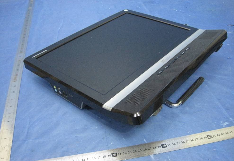
Click to zoom
Application Details
- Equipment Class
- JBC - Part 15 Class B Computing Device/Personal Computer
- Date of Grant
- Mar 30, 2010
- Application Purpose
- Original Equipment
- Date of Application
- Mar 30, 2010
- Equipment Note
- PC ALL IN ONE
- Country
- Hong Kong
Documents & Files
Document Text
Text extracted from the exhibit documents filed with the FCC. Open a document above to read the original.
Users Manual
PCALLINONE UserManual Thankyouforbuyingthisproduct-themostfashionablePCallinone.ToenjoyyourPCall inonetothefullfromtheverybeginning,pleasereadthismanualcarefullyandkeepit handyforfuturereference. Gatheryourcomputerandthepartsasshownintheillustration.You'llneedtheseto completethestepsforthecomputerset-upprocedurethatfollow,ifyoufoundanylost, pleasecontactwiththedistributorandaskforthem. UNPACKINGTHEBOXCONTENTS ComputerKeyboard MouseDriverCDPowercord Poweradapter Usermanual Qualitycertificate Qualitycertificate Frontview(1) Keysinstruction: 1.AUTO:Toresizedisplayareatofitforfullscreenofpanel.OrtoexitSETUPmenu. 2.MENU:ToenterMENUsettingmode,ortoconfirmmenusetting 3.-:Volumedownormovedownthehighlightbarduringmenusetting 4.+:Volumeupormoveupthehighlightbarduringmenusetting 5.MUTE:Tomutetwobuilt-infrontspeakersofthecomputer,butkeepsoundoutput statusofsideLineoutjack. 6.POWER:Topoweronorpoweroffthecomputer 7.HDDindicator(BlueLEDlight):ToshowtheworkingstatusoftheHDD 8.POWERindicator(YellowLEDlight):ToshowtheworkingstatusofthePOWERof computer. 12 Keys instruction: Front view (2) 1. AUTO: To resize display area to fit for full screen of panel. Or to exit SETUP menu.2. MENU: To enter MENU setting mode, or to confirm menu setting3. -: Volume down or move down the highlight bar during menu setting4. +: Volume up or move up the highlight bar during menu setting5. MUTE: To mute two built-in front speakers of the computer, but keep sound output status of side Line out jack. 6. POWER: To power on or power off the computer7. HDD indicator(Blue LED light): To show the working status of the HDD8. POWER indicator(Yellow LED light): To show the working status of the POWER of computer. 1 32 6 7 Left view 1.Line in/Rear speaker2.Line out/Front speaker3.Microphone/Center speaker4.KEYBOARD5.MOUSE6.RJ45(LAN)7.USB 1/2/3/4 1 2 3 4 5 6 7 8 34 Keys instruction: 4 5 1 2 3 4 5 Rearview(withexternalpowersupply) Rearview 1.USB5/6 2.POWERSWITCH(ON/OFF):theGeneralPowerswitchbutton 3.DCjackforDCterminaloftheAdapter 4.Computerstand 5.VentilationholeforFAN 6.Opticaldiscdrive(ODDdrive) Note: 1.Thepictureillustratedaboveisforreferenceonly.Theactualspecificationor appearancemaybedifferentsubjecttorequirementsofthecustomer. 2.TherearetwokindsofOpticaldiscdrivesforthiscomputer,itdependsonyour specification,oneisslimtrayODD,andtheotherisslimslot-inODD,FortrayODD, PleasepressEXITbuttontopop-upthetray,andthenputthediscwithnon-dataside facingyou,andthenpushthetray.Forslimslot-inODD,pleaseinsertthediscdirectly withnon-datasidefacingyou,toexitthedisc,presstheEXITbutton. QuickstartGuide Step1.Unpackthegiftboxcontentstogatheryourcomputerandrelevantaccessories, thenpositionthecomputerinasuitableplace,insertDCterminaloftheadaptertoDC jackofthecomputer,andfinallyfinishtheconnectionbetweenadapterandwalloutlet. Step2.InserttheUSBterminalsofkeyboardandmousetotheUSBportinthebackofthe computer. Step3.SwitchonthePOWERSWITCHatthebackofthecomputer.PressPOWER buttononthefrontkeypadofthecomputertoturnonthecomputer,andinsertthe OS(operatingsystem)installationdisctotheODDdrive,thecomputerwillbootfromthe disc,pleasefinishtheinstallationofOSbyfollowingtheinstallationguideoftheOS installationCD. Step4.AfterinstallationoftheOS,pleaseinsertthedriverCDintotheODDdriveand choosethesuitabledriversforyourOStoinstall,pleasefollowthestepsshownbelowfor drivers'installation,andrestartyourcomputerafterinstallation. 1.M/Bdriver(driverformotherboardchipset) 2.VGAdriver(driverforbuilt-inVideoprocessingcard) 3.Sounddriver(driverforsoundchipset) 4.LANdriver(driverforlocalnetworkcard) 5.WIFIdriver(driverforwirelessnetworkcard) Note:PleasemakesurethecomputerisatPOWEROFFstatuswhenyouconnectthe cableorterminaltothecomputereachtimebyswitchingoffthePOWERSWITCH atthebackofthecomputer. Note:ThecomputerBIOSdefaultbootsequenceisfromODDdrive,ifyoufailedto bootthecomputerfromthenormalbootdiscorOSinstallationdiscwhichisinserted totheODDdrive,firstpleasecheckifthereareanyproblemswithyourdisc,orelse, pressCTRL+ALT+DELETEtorestartthecomputer,andholdDELETEkeyfora fewsecondstoentertheBIOSsettinginterfaceduringBIOSPOST(power-on-self- test)procedure,andthenpressF9andENTERtoloadtheoptimaldefaults,press F10andENTERtosaveconfigurationchangesandexitsetup,thecomputerwill restartonceagainandtrytosearchbootdiscsfromtheODDdriveandbootthe computer. NOTE:Pleaseinstalltheproperdriversforyourcomputerbasingonthe specificationofyourcomputer. 5 6 Step 5. Please set resolution of your operating system to 1440*900@60HZ, and theninstall your softwares and enjoy our fashionable computer.Step 6. To power off the computer, please follow these steps, firstly, turn off the operatingsystem, secondly, press the POWER switch on the back of the computer. If you can't turnoff the operating system, please press the POWER button for four seconds and thecomputer will be forced to shut down, and two seconds afterwards, the computer willrestart once again.NOTE:1.After installation of the sound driver, the default sound player of the computer istwo built-in front speakers of computer. If you want to use external activeloudspeaker, please connect the terminal to LINE OUT jack of the computer andpress MUTE key on the front keypad to mute the built-in front speakers. After thecomputer enter power saving mode or standby mode, the built-in front speakers willstop working temporarily, if you want to play music under these modes, please use anexternal active loudspeaker.2.After initial installation of the sound driver, the default setting of the microphoneis mute, please turn on it manually before using it. 7 FCC NOTE: This device complies with Part 15 of the FCC Rules. Operation is subject to the followingtwo conditions:(1)this device may not cause harmful interference, and (2) this devicemust accept any interference received, including interference that may cause undesiredoperation. The manufacturer is not responsible for any radio or TV interference caused by unauthorized modifications to this equipment. Such modifications could v…
Text truncated - open the document above for the full version.
Cover Letter(s)
STARVF(CHINA)TECHNOLOGY COMPANY LIMITED. FCC ID: X9GPP17X POWER OF ATTORNEY March.20, 2010 Federal Communications Commission Authorization and Evaluation Division 7435 Oakland Mills Road Columbia, MD 21046 To Whom It May Concern: We, the undersigned, hereby authorize Waltek Services (ShenZhen) Co., Ltd. (Philo Zhong) on our behalf, to apply to the Federal Communications Commission on our equipment. Any and all acts carried out by Waltek Services (ShenZhen) Co., Ltd. (Philo Zhong) on our behalf shall have the same effect as acts of our own. This authorization expires on March.21,2011 This is to advise that we are in full compliance with the Anti-Drug Abuse Act. We, STARVF(CHINA)TECHNOLOGY COMPANY LIMITED..are not subject to a denial of federal benefits pursuant to Section 5301 of the Anti-Drug Act of 1988, 21 USC853a, and no party to the application is subject to a denial of federal benefits pursuant to that section. Sincerely, STARVF(CHINA)TECHNOLOGY COMPANY LIMITED.. .................................... Manager
External Photos
STARVF(CHINA)TECHNOLOGY COMPANY LIMITED. FCC ID: X9GPP17X Page:19 of 24 5 Photographs - Constructional Details 5.1 EUT - Front View 5.2 EUT – Back View
ID Label/Location Info
STARVF(CHINA)TECHNOLOGY COMPANY LIMITED. FCC ID: X9GPP17X Page:24 of 24 FCC ID Label This device complies with Part 15 of the FCC Rules. Operation is subject to the following two conditions:(1)this device may not cause harmful interference, and (2) this device must accept any interference received, including interference that may cause undesired operation. The Label must not be a stick-on paper. The Label on these products must be permanently affixed to the product and readily visible at the time of purchase and must last the expected lifetime of the equipment not be readily detachable. Proposed Label Location on EUT EUT Top View/ proposed FCC Label Location FCC ID: X9GPP17X This device complies with Part 15 of the FCC Rules. Operation is subject to the following two conditions:(1)this device may not cause harmful interference,and (2) this device must accept any interference received, including interference that may cause undesired operation
ID Label/Location Info
FCC ID Label Sample for Model: PP17X(X=A-Z,stands for differernt appearance) FCC ID : X9GPP17X This device complies with Part 15 of the FCC Rules. Operation is subject to the following two conditions:(1)this device may not cause harmful interference, and (2) this device must accept any interference received, including interference that may cause undesired operation.
Internal Photos
STARVF(CHINA)TECHNOLOGY COMPANY LIMITED. FCC ID: X9GPP17X Page:21 of 24 5.5 PCB 1 -Front View 5.6 PCB 1 - Back View STARVF(CHINA)TECHNOLOGY COMPANY LIMITED. FCC ID: X9GPP17X Page:22 of 24 5.7 PCB 2 -Front View 5.8 PCB 2 –Back View STARVF(CHINA)TECHNOLOGY COMPANY LIMITED. FCC ID: X9GPP17X Page:23 of 24 5.9 PCB 3 -Front View 5.10 PCB 3 -Back View
Operational Description
Circuit Description The PC ALL IN ONE ,which use the alternating current, it can be adjusted from AC 120V to DC 12V by external power adapter , and input to the machine by the port of 12V DC input , and then down to 3.3V ,5V -3.3V,-5V by DC POWER MODULE , supply the power to the motherboard of computer and A/D board . the power output and power close for DC POWER MODULE can be controlled by computer motherboard . the motherboard working power is suited to the ATX power standard , A/D board need 12V DC , and switch it into 12V , 5V ,3.3V ,1.8V to main chipset , amplifier ,inverter.Inverter function is that it can light up the panel, 12V DC is switched to 1600V AC, 2 seconds late, it output 600-1000V AC. the main chipset of A/D board can control the output voltage and voltage turn on/turn off, and protect if over-voltage and seeping-carry.When we press the power switch, DC power supply unit modules began to computer motherboards and A / D board equipment, power supply voltage is not stable at this time, the motherboard chipset to the CPU control the issue and maintain a RESET (re - set) signals, so that CPU initialization. When the power supply began to stabilize after the (of course, the process from unstable to stable is only a brief moment), will be removed RESET signal chip set, CPU immediately at the beginning from the address FFFF0H execution.A/D board, after receiving the power to carry out RESET MCU book value loaded, A/D board automatically working condition, LCD backlight has been lit, waiting for input.The computer board system BIOS boot code start POST (Power On Self Test), POST is mainly the detection system some of the key equipment for the existence and ability to work, such as memory and graphics cards. If not found there is a problem of memory or the memory, when the system PIOS audible through the loudspeaker to report error conditions. Then the system BISO will find graphics card, BIOS, graphics card BIOS stored in ROM chip, usually starting address C0000H Department, the computer system BIOS calls to find it after the video card BIOS initialization code to complete the display by the graphics card BIOS initialization. Then the system BIOS looks for other devices of the BIOS program, find the same want to call them after the BIOS initialization code to initialize the house such equipment.When all other equipment to check BIOS, the system BIOS will display its own splash screen, this time Computer board "VGA OUTPUT" normal waveform output, A/D board "VGA INPUT" side, after receiving the waveform from the master chip waiting to enter the work state, through the ADC (analog-digital conversion signals) module, after processing into the output of flat-panel TVs SCALER module can accept flat-panel image display data formats,which the working frequency is 533Mhz, LCD flat-panel image display data received by the internal timing control electric swagger converted driven LCD screen display the correct video image. At this point the computer panel output information includes the type of system BIOS serial number and version number and so on. At the same time lower left corner of the screen will appear at the bottom of the motherboard information code that contains the date BIOS, motherboard chipset, model, motherboard identification code and vendor code.And then the system BIOS will detect the CPU type and operating frequency, and test results displayed on the screen. Then the system BIOS to start testing all of the memory capacity of the host and simultaneously displayed on the screen memory test values.The memory test, the system BIOS installed on the system will begin testing a number of standard hardware devices, these devices include: hard drives, CD-ROM, floppy drive, serial interface and parallel interface to connect devices.
Schematics
55 44 33 22 11 D D C C B B A A 12VIN 5V AUD_R AMP_12V AUD_L AUD_RAUD_L BKLTON MUTE_VCC AUD_PWM SH3 AUD_MUTE SH3 BKT_PWM SH3 PBIAS SH3 GND 12V GND GND GND GND GND GND 5V 5V 3.3V GND 3.3V 1.8V GND GND GND GND GND GND 5V 12V GND GND MUTE_VCC GND GND GND GND GND 5V GND GND 5V GND 12V GND GND GNDGND GNDGND 5V AMP_12V GND TitleSize Document Number Rev Date: Sheet of <Doc> <RevC o <Title> A4 13 Saturday, August 29, 2009 TitleSize Document Number Rev Date: Sheet of <Doc> <RevC o <Title> A4 13 Saturday, August 29, 2009 TitleSize Document Number Rev Date: Sheet of <Doc> <RevC o <Title> A4 13 Saturday, August 29, 2009 R24 2.2K R24 2.2K 123 CN4 CON3-DIP/2.0MM CN4 CON3-DIP/2.0MM R1910K_NMR1910K_NM R25 510R_NM R25 510R_NM FB 1 EN 2 OCSET 3 VIN 4 OUT 5 OUT 6 GND 7 GND 8 U1 AP1534U1 AP1534 E5 220uF/16V_SK E5 220uF/16V_SK R447KR447K E1 220uF/16V_GL E1 220uF/16V_GL C3 100nF_Y C3 100nF_Y 12 D1SR34D1SR34 FB4 FB0805 FB4 FB0805 1 2345 6 6 7 7 8 8 9 9 H2 H8-D8/3.5 H2 H8-D8/3.5 1 32 Q2 3904 Q2 3904 R11 330R R11 330R FB2 FB1206 FB2 FB1206 R21 10K_NM R21 10K_NM 1 23 Q33906_NMQ33906_NM IN 3 GND 1 OUT 2 TAB 4 U3LDO/1117-1.8VU3LDO/1117-1.8V FB1 MGRH3560 FB1 MGRH3560 GND 1 GND 2 INR 9 INL 4 SVR 10 VOL 6 VAO_L 5 OUTL 17 MUTE 12 STBY 11 OUTR 14 Vs 15 Vs 16 VAO_R 7 GND 3 GND 13 GND 18 GND 19 GND 20 NC 8 U4 AMP/TDA7496L U4 AMP/TDA7496L 1234 CN2CON4-DIP/2.0MMCN2CON4-DIP/2.0MM 1234 CN5 CON4-DIP/2.0MM CN5 CON4-DIP/2.0MM 1 1 2 2 3 3 4 4 5 5 6 6 CN6 CON6-DIP/2.0MM CN6 CON6-DIP/2.0MM 1 1 2 2 3 3 CN1 DC12V/5A_D2.0MM CN1 DC12V/5A_D2.0MM C191uF_YC191uF_Y C8 100nF_X C8 100nF_X R34.7KR34.7K 1 2345 6 6 7 7 8 8 9 9 H1 H8-D8/3.5 H1 H8-D8/3.5 R18 0R R18 0R R26 0R R26 0R R142.2KR142.2K FB5 FB1206 FB5 FB1206 C10 100nF_Y C10 100nF_Y C12 1uF_Y C12 1uF_Y C7 100nF_X C7 100nF_X 12345 CN3 PJ-317-5P CN3 PJ-317-5P C2 100nF_Y C2 100nF_Y C171uF_YC171uF_Y R17 1K R17 1K R23 10K_NM R23 10K_NM FB6 MGRH3560 FB6 MGRH3560 FB3 FB0805 FB3 FB0805 R16 4.7K R16 4.7K R5 4.7KR5 4.7K C201uF_YC201uF_Y R9 4.7K_NM R9 4.7K_NM C1 100nF_Y C1 100nF_Y R22 0R R22 0R E9 220uF/16V_SK E9 220uF/16V_SK F1 5A F1 5A E6 220uF/16V_SK E6 220uF/16V_SK E4 220uF/10V_GL E4 220uF/10V_GL L1 33uH L1 33uH R15 47K R15 47K C14 1nF_X C14 1nF_X C4 100nF_Y C4 100nF_Y C5 10nF_X C5 10nF_X E7 220uF/10V_GL E7 220uF/10V_GL R6 4.7KR6 4.7K E8 220uF/10V_GL E8 220uF/10V_GL C13 1uF_Y C13 1uF_Y C9 100nF_X C9 100nF_X R10 4.7K_NM R10 4.7K_NM R2 1K/1% R2 1K/1% R810K_NMR810K_NM C15 1nF_X C15 1nF_X R74.7KR74.7K 1 32 Q4 3904 Q4 3904 R12K/1%R12K/1% E3 100uF/10V_GL E3 100uF/10V_GL C18 100nF_X C18 100nF_X R12 4.7K R12 4.7K IN 3 GND 1 OUT 2 TAB 4 U2 LDO/1084-3.3V U2 LDO/1084-3.3V 1 2345 6 6 7 7 8 8 9 9 H3 H8-D8/3.5 H3 H8-D8/3.5 R13100RR13100R 1 2345 6 6 7 7 8 8 9 9 H4 H8-D8/3.5 H4 H8-D8/3.5 C161uF_YC161uF_Y 1 32 Q1 3904 Q1 3904 R204.7KR204.7K E2 220uF/10V_GL E2 220uF/10V_GL C6 100nF_X C6 100nF_X C11 100nF_Y C11 100nF_Y 55 44 33 22 11 D D C C B B A A VGA_B+ VGA_B- VGA_G+ VGA_G- VGA_R+ VGA_R- VGA_SCLVGA_VSVGA_HSVGA_SDA VGA_B+VGA_B-VGA_G+VGA_G-VGA_R+VGA_R-VGA_SCLVGA_SDAVGA_HSVGA_VS SCLSDA VGA-SDAVGA-SCL VGA_SCLVGA_SDA DDC_SDADDC_SCL VGA_R+ R+R- VGA_G+ G+G- VGA_B+ B+B- HSYNC VGA_HSVGA_VS VSYNC R+ SH3 R- SH3 G+ SH3G- SH3B+ SH3B- SH3HSYNC SH3 VSYNC SH3 DDC_SCL SH3 DDC_SDA SH3 GND VGA_5V GND VGA_5V 5V GND GND GND GND GND GND GND GND GND GND GND TitleSize Document Number Rev Date: Sheet of <Doc> <RevC o <Title> A4 23 Saturday, August 29, 2009 TitleSize Document Number Rev Date: Sheet of <Doc> <RevC o <Title> A4 23 Saturday, August 29, 2009 TitleSize Document Number Rev Date: Sheet of <Doc> <RevC o <Title> A4 23 Saturday, August 29, 2009 1 2 3 6 7 8 12 15 13 14 5 10 R49 0R R49 0R NP ZD1 1 NP ZD1 1 R27 47R R27 47R C26 100nF_X C26 100nF_X C21 100nF_X C21 100nF_X NP ZD4 1 NP ZD4 1 R32 47R R32 47R C24 100nF_X C24 100nF_X R39 2.2K R39 2.2K NP ZD7 1 NP ZD7 1 R48 33R R48 33R NP ZD5 1 NP ZD5 1 123456789 101112 CN8 CON12-DIP/2.0MM CN8 CON12-DIP/2.0MM R42 4.7K R42 4.7K R4033RR4033R R36 47R R36 47R R38 2.2K R38 2.2K R46 N10K_NM R46 N10K_NM R4133RR4133R R33 47R R33 47R R34 75R R34 75R R30 47R R30 47R C25 100nF_X C25 100nF_X R45 33R R45 33R NP ZD6 1 NP ZD6 1 NP ZD3 1 NP ZD3 1 R37 47R R37 47R C28 33pF_NPO C28 33pF_NPO R44 33R R44 33R R43 4.7K R43 4.7K R31 75R R31 75R C23 100nF_X C23 100nF_X C29 100nF_X C29 100nF_X NP ZD2 1 NP ZD2 1 A0 1 A1 2 A2 3 GND 4 SDA 5 SCL 6 WP 7 VCC 8 U5 24XX02 U5 24XX02 3 1 2 D2 BAT54C D2 BAT54C 162738495 1112131415 10 1716 CN7 VGA/DB15 CN7 VGA/DB15 R47 33R R47 33R C27 33pF_NPO C27 33pF_NPO R29 47R R29 47R C22 100nF_X C22 100nF_X R35 47R R35 47R R28 75R R28 75R 55 44 33 22 11 D D C C B B A A SPI_CSnSPI_DI SPI_CLKSPI_DO TXDRXD GPO3GPO2 GPO3GPO2GPO1 SPI_CSnSPI_CLKSPI_DISPI_DO AUD_PWMBKT_PWMGPO3GPO2GPO1AUD_MUTESPI_CSn GPIO_8GPIO_9GPIO_10SDA_RDSCL_TDG_LEDR_LEDATX0+ATX0-ATX1+ATX1-ATX2+ATX2-ATX3+ATX3-ATCK+ATCK-BKX0+BKX0-BKX1+BKX1-BKX2+BKX2-BKX3+BKX3-BTCK+BTCK- PPWRPBIAS LBADC_IN1 RIGHTLEFTON/OFFAUTOMENUEXIT/SELECT ON/OFFRED_LEDGREEN_LEDRIGHTLEFTAUTOMENUEXIT/SELECT R_LEDG_LEDPPWR ATX0-ATX1-ATX2-ATCK-ATX3-BKX0-BKX1-BKX2-BTCK-BKX3- ATX0+ATX1+ATX2+ATCK+ATX3+BKX0+BKX1+BKX2+BTCK+BKX3+ GPIO_10GPIO_9GPIO_8 SCLSDA R+ SH2 R- SH2 G+ SH2 G- SH2 B+ SH2 B- SH2 HSYNC SH2 VSYNC SH2 DDC_SCL SH2 DDC_SDA SH2 BKT_PWM SH1 AUD_PWM SH1 AUD_MUTE SH1 PBIAS SH1 3.3V GND 3.3V_APL 3.3V GND 3.3V_AVD 3.3V GND 3.3V_ALV 1.8V_DVD GND 1.8V_AVD 3.3V GND 3.3V_DVD 1.8V GND 1.8V_DVD GND 3.3V_DVD 3.3V_DVD GND 5V GND 3.3V_APL 3.3V_DVD GND 3.3V_DVD GND GND 3.3V_APL 3.3V_AVD 3.3V_ALV 3.3V_DVD 1.8V_DVD 1.8V_AVD GND GND 3.3V_DVD GND GND 3.3V 5V 12V GND LCDPWR GND LCDPWR GND GND 3.3V_DVD GND 5V GND TitleSize Document Number Rev Date: Sheet of <Doc> <RevCode> <Title> Custom 33 Saturday, August 29, 2009 TitleSize Document Number Rev Date: Sheet of <Doc> <RevCode> <Title> Custom 33 Saturday, August 29, 2009 TitleSize Document Number Rev Date: Sheet of <Doc> <RevCode> <Title> Custom 33 Saturday, August 29, 2009 1 2 3 4 5 6 CN11 CON8-PDIP/2.54MM-L CN11 CON8-PDIP/2.54MM-L FB10 FB0603 FB10 FB0603 C57 100nF_X C57 100nF_X R59 2.2KR59 2.2K C53 10nF_X C53 10nF_X NP ZD8 1 N…
Text truncated - open the document above for the full version.
Test Report
STARVF(CHINA)TECHNOLOGY COMPANY LIMITED.. FCC ID: X9GPP17X FCC TEST REPORT Page: 1 of 26 FCC ID : X9GPP17X Applicant : STARVF(CHINA)TECHNOLOGY COMPANY LIMITED. Address : PLAT/RM603, 6/F, SUMMIT INSURANCE BUILDING, 789NATHAN ROAD, MONGKOK KOWLOON, H.K. Equipment Under Test (EUT) : Product description : PC ALL IN ONE Model No. : PP17X(X=A-Z,stands for differernt appearance) Standards : FCC Part 15 Subpart B Date of Test : March 22, 2010 Test Engineer :Olic.huang Reviewed By : Test Result : PASS * PERPARED BY: Waltek Services (Shenzhen) Co., Ltd. 1/F, Fukangtai Building,West Baima Rd.,Songgang Street, Baoan District, Shenzhen 518105,China Tel :+86-755-27553488 Fax:+86-755-27553868 . STARVF(CHINA)TECHNOLOGY COMPANY LIMITED. FCC ID: X9GPP17X Page:2 of 26 1 Test Summary Test Test RequirementTest Method Class / Severity Result Radiated Emission (30MHz to 5GHz) FCC PART 15, SUBPART B: 2008 ANSI C63.4: 2009 Class B PASS Conducted Emission (150KHz to 30MHz) FCC PART 15, SUBPART B: 2008 ANSI C63.4: 2009 Class B PASS STARVF(CHINA)TECHNOLOGY COMPANY LIMITED. FCC ID: X9GPP17X Page:3 of 26 Contents 1 COVER PAGE......................................................................................................................................................... 1 1 TEST SUMMARY .......................................................................................................................................................... 2 CONTENTS ......................................................................................................................................................................... 3 2 GENERAL INFORMATION ................................................................................................................................... 4 2.1 CLIENT INFORMATION.............................................................................................................................................. 4 2.2 GENERAL DESCRIPTION OF E.U.T. ........................................................................................................................... 4 2.3 DETAILS OF E.U.T. .................................................................................................................................................. 4 2.4 DESCRIPTION OF SUPPORT UNITS............................................................................................................................. 4 2.5 STANDARDS APPLICABLE FOR TESTING................................................................................................................... 4 2.6 TEST FACILITY......................................................................................................................................................... 5 2.7 TEST LOCATION....................................................................................................................................................... 5 3 EQUIPMENT USED DURING TEST..................................................................................................................... 6 4 EMISSIONS TEST RESULTS ................................................................................................................................. 9 4.1 CONDUCTED EMISSION DATA.................................................................................................................................. 9 4.1.1 E.U.T. Operation ........................................................................................................................................... 9 4.1.2 EUT Setup.................................................................................................................................................... 10 4.1.3 Conducted Emission Test Data.................................................................................................................... 11 4.1.4 Photographs – Conducted Emission Test Setup .......................................................................................... 13 4.2 RADIATION EMISSION DATA.................................................................................................................................. 14 4.2.1 Measurement Uncertainty ........................................................................................................................... 14 4.2.2 EUT Setup.................................................................................................................................................... 14 4.2.3 Spectrum Analyzer Setup ............................................................................................................................. 15 4.2.4 Test Procedure............................................................................................................................................. 15 4.2.5 Corrected Amplitude & Margin Calculation............................................................................................... 17 4.2.6 Summary of Test Results.............................................................................................................................. 17 4.2.7 Photographs – Radiation Emission Test Setup............................................................................................ 20 5 PHOTOGRAPHS - CONSTRUCTIONAL DETAILS ........................................................................................ 21 5.1 EUT - FRONT VIEW............................................................................................................................................... 21 5.2 EUT – BACK VIEW................................................................................................................................................ 21 5.3 ACCESSORIES – APPEARANCE VIEW...................................................................................................................... 22 5.4 EUT- OPEN VIEW...........................................................................…
Text truncated - open the document above for the full version.
Test Setup Photos
STARVF(CHINA)TECHNOLOGY COMPANY LIMITED. FCC ID: X9GPP17X Page:20 of 26 4.2.7 Photographs – Radiation Emission Test Setup Below 1G Above 1G Photographs – Conducted Emission Test Setup
Contact Information
Applicant
MARK MENG(MANAGER)
Test Firm
Waltek Services(Shenzhen) Co., Ltd.Philo zhong
Technical Specifications
| # | Rule Parts | Frequency Range | Power Output |
|---|---|---|---|
| 1 | 15B | - | - |