XQ3WDTWireless data communication system
PATLITE Corporation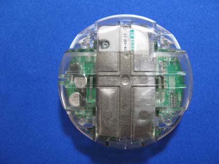
Click to zoom
Application Details
- Equipment Class
- DTS - Digital Transmission System
- Date of Grant
- Aug 24, 2010
- Application Purpose
- Original Equipment
- Date of Application
- Aug 24, 2010
- Equipment Note
- Wireless data communication system
- Frequency Range
- 2405.00000000 - 2480.00000000
- Company
- PATLITE Corporation
- Country
- Japan
Documents & Files
Document Text
Text extracted from the exhibit documents filed with the FCC. Open a document above to read the original.
Users Manual
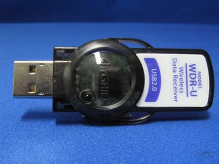
Protective structure All directions * Connected to the USB port of the PC The recommended number is 20. (It differs depending on the installation location and the communication environment.) In compliance with the installed signal tower Protective structure This symbol indicates what the user MUST NOT DO (Prohibited). Thank you for purchasing the wireless data communication system. Read this instruction manual carefully prior to use. This manua l contains information to ensure correct use. Keep this instruction manual in a safe place. Also read this manual when maintenance, an inspection, or repai r is needed. If you have any questions, contact one of the sales offices or the technical center listed on the last page. Wireless Data Communication System Instruction Manual TYPE: WD 8144-A T95100126 Warning -Safety Precautions- ◆This manual classifies the precautions into the following two categories depending on the degree of injury or damage caused by failure to follow them: Warning Caution Failure to follow a warning may cause death or serious injury. Failure to follow a caution may cause personal injury or physic al damage. ◆The meanings of symbols used in this manual are as shown below : This symbol indicates what the user MUST DO (Mandatory). To prevent injury to the user or other people and property dama ge, the following precautions must be observed. - Do not disassemble or modify the product. Failure to follow t his instruction may cause fire or electric shock.- Do not use the product where condensation can form. Failure t o follow this instruction may cause fire or electric shock.- Do not use or install the receiver (WDR-L/U) near water or ot her liquids, in a place where oil may spatter, or in a moist or dusty place. F ailure to follow this instruction may cause fire, electric shock, or malfunction.- Do not use this product near pacemakers or electric medical e quipment because radio waves may affect these devices and equipment.- This product is not intended to be installed in or control fa cilities or equipment affecting human lives, including medical equipment, nuclear facilities and equipment, aerospace equipment, and transportation facilities and equip ment, and facilities and equipment requiring high reliability. We assume no responsib ility for any accident causing injury or death or property damage arising from use of this product with such facilities, equipment, or control systems.- Turn off this product in airplanes, hospitals, or other place s where radio waves may affect surrounding equipment or the use of wireless devi ces is prohibited. - The receiver (USB connection type: WDR-U) is driven by power supplied by a USB bus. Connect it to a USB port. Using it with other ports may cause fire, electric shock, or smoke.- Turn off the product during wiring or installation. Failure t o follow this instruction may cause an electric shock.- Ensure that the power supply voltage does not exceed the allo wable voltage range. Failure to follow this instruction may cause fire or malfunction. - If the installation of this product involves construction wor k, have it installed by a professional. Failure to follow this instruction may cause f ire, electric shock, or fall. - If smoke, odor, or other abnormalities are present, immediate ly stop supplying power to this product. Using it under such abnormal conditio ns may cause fire or electric shock. Caution - Do not splash any liquid onto the receiver (WDR-L/U) nor brin g it into contact with metal objects. Failure to follow this instruction may caus e fire or electric shock. - Ensure that the polarity of the power supply is correct. Inco rrect polarity may cause a malfunction.- Do not use this product near fire, in a hot and humid place, or in a place where a corrosive or combustible gas is generated. Failure to follow this instruction may cause a malfunction, preventing the product from working pro perly. Do not use or store this product in the following places. Doing so may cause a glitch or malfunction.- Poorly ventilated places - Near fire or a hot and humid pl ace - Near equipment that generates an intense electric field or fe rromagnetic field - A place subject to direct sunlight - A place subject to sh ock and vibration - Near heating devices - A place where a lot of dust or iron powder is generated - A place from which the product is likely to fall - A place exposed to salt air Pay attention to the following precautions:- Because of the nature of radio waves, noise or casing may mak e it impossible to establish communication even within the access range.- Do not eat, drink, or smoke near this product. Food or bevera ges or cigarette ashes may cause a malfunction.- Do not use chemicals near this product. Some chemicals may ca use the product to melt or deform if they come into contact with it. We assume no liability for any malfunction arising from failure to observe these warnings or cautions, disassembling or modification, or natural disasters. Do not use this product for purposes other than those specified in this manual. 2. URLs for downloads2 . U R L s f o r d o w n l o a d s Download the General Instruction Manual and the application sof tware driver from one of our websites. Download them according to the instruction of the screen after clicking the WD banner. URL : http://www.patlite.com/ 3. Part names3 . P a r t n a m e s a) Transmittera) Transmitter 5. Usage5 . U s a g e Be sure to refer to the General Instruction Manual for the usag e instructions. * Refer to the General Instruction Manual for the detailed spec ifications and compatible signal towers.* The specifications are subject to change due to improvement w ithout notice. 6. Specifications6 . S p e c i f i c a t i o n s a) Transmitter Install the transmitter according to the drawing below. This drawing is a reference drawing for the LE series. The LME series has a dedicated bracket.b) Receiver Install and wire the WDR-L according to the drawing below. Connect the…
Text truncated - open the document above for the full version.
Cover Letter(s)
PCB for testing (Transmitter WDT) Since the actual product (below photo) can not be designed neccesary setting or operation for testing, the test was performed with the PCB which has the interface board set for the test. About the both PCB, since RF module parts circled by red is the same between PCB for testing and the actual product, we judged the same result could be got on Conducted measurement test. The actual product (Transmitter WDT)
Cover Letter(s)
ZB24FM-Z I/F-Board (Interface Board) Following is explanation about ZB24FM-Z I/F-Board (Interface Board). The interface board is connected with ZB24FM-Z2501 and it is used for testing of communication test and easy sensor operation etc easily. Since the interface board is designed and made for the test, please do not use except testing. (Do not ship product for customer with the interface board.) Summary of Function The board is connected with ZB24FM-Z2501 and it can be communicated with RS-232C cable (straight). Communication operation test can be performed by LED, SW and temperature sensor by using attached application software. It makes it easy that connecting test with exterior system or exterior sensor etc by 4-20mA I/F and photo MOS relay. Block diagram Level converter Photo MOS relay Temperature sensor sensor Power Supply Sleep release
Cover Letter(s)
i66e ttg'r +Mw1efi7t ))\-rrs z €;80?e 56e770? FEDERAL COMMLNICATIONS COMMISSION 7435 OaIIed Mills Road Slbjecr Declaolion ofth€ model ditrerenoes FCCID:XO3WDT wq PATLITE CORPORATION, hereby deolare thal ths difeEn€ belw€en Models WDT-6M md WDT-58 is only the dianeter for or the enclosure, and bo$ models use the sme wi€lss module, inside tbe PWB (Printed-Wiring Board) and lbe sde materials Theclore, Models WDT'6M and WDT 5E.E identical.
External Photos
PATLITE CORPORATION 19-2,TECHNO PARK,SANDA,HYOGO,669-1339 TEL:81-79-568-7707 FAX:81-79-568-7737 〒669-1339 兵庫県三田市テクノパーク19-2 電話079-568-7707 FAX:079-568-7737 WDT-6M and WDT-5E Photograph drawing External photo WDT-6M upside (Same as WDT-5E) WDT-6M upside without cover (Same as WDT-5E) WDT-6M front side WDT-5E front side
Internal Photos
PATLITE CORPORATION 19-2,TECHNO PARK,SANDA,HYOGO,669-1339 TEL:81-79-568-7707 FAX:81-79-568-7737 〒669-1339 兵庫県三田市テクノパーク19-2 電話079-568-7707 FAX:079-568-7737 WDT-6M and WDT-5E Photograph drawing Internal photo WDT-6M PCB component side (Same as WDT-5E) WDT-6M PCB soldering side (Same as WDT-5E) PATLITE CORPORATION 19-2,TECHNO PARK,SANDA,HYOGO,669-1339 TEL:81-79-568-7707 FAX:81-79-568-7737 〒669-1339 兵庫県三田市テクノパーク19-2 電話079-568-7707 FAX:079-568-7737 WDT-6M RF module component side (Same as WDT-5E) WDT-6M RF module soldering side (Same as WDT-5E) PATLITE CORPORATION 19-2,TECHNO PARK,SANDA,HYOGO,669-1339 TEL:81-79-568-7707 FAX:81-79-568-7737 〒669-1339 兵庫県三田市テクノパーク19-2 電話079-568-7707 FAX:079-568-7737 * RF module is same as above WDT-6M PCB component side for testing(Same as WDT-5E) WDT-6M PCB soldering side for testing(Same as WDT-5E)
RF Exposure Info
Prediction of MPE limit at a given distance Equation from page 18 of OET Bulletin 65, Edition 97-01 Equipment WDT-6M, WDT-5E Manufacturer PATLITE CORPORATION where: S = power density P = power input to the antennaG = power gain of the antenna in the direction of interest relative to an isotropic radiator R = distance to the center of radiation of the antenna Maximum peak output power at antenna input terminal: 3.07 Maximum peak output power at antenna input terminal: 2.02768272 Antenna gain(typical): 1.64 Maximum antenna gain: 1.45881426 (numeric) Prediction distance: 20 (cm) Prediction frequency: 2440 (MHz) MPE limit for uncontrolled expos ure at prediction frequency: 1 Power density at prediction frequency: 0.000588 Maximum allowable antenna gain: 33.94269855 Margin of Compliance: 32.30269855 (dBm)(mW)(dBi)(mW/cm^2)(mW/cm^2)(dBi) 2 4 R PG S π =
Test Report
Page 2 of 54 Test Report No. R094435-1 List of Contents Page 1. Description of Equipment Under Test ............................................................................................4 1.1 Product Description ....................................................................................................................4 1.2 Antenna Description...................................................................................................................4 1.3 Accompanied Peripherals Description .......................................................................................4 2. General Information ...........................................................................................................................5 2.1 Test Methodology ........................................................................................................................5 2.2 Test Facility ................................................................................................................................5 2.3 Traceability .................................................................................................................................5 3. Summary of Test Results ...................................................................................................................6 4. Test Configuration ..............................................................................................................................7 4.1 15. 207 AC Power Conducted Emission in Shield Room.........................................................7 4.2 15. 247(d), 15.209 Transmitter Radiated Emissions, 15.209 Band Edge (Radiated), and 15.215 (c) 20 dB Bandwidth in 3m Anechoic Chamber .....................................................................8 4.3 Test Mode..................................................................................................................................8 5. Measurement Result...........................................................................................................................9 5.1 15. 207 AC Power Conducted Emission...................................................................................9 5.1.1 Setting Remarks ................................................................................................................9 5.1.2 Minimum Standard ...........................................................................................................9 5.1.3 Result .................................................................................................................................9 5.1.4 Measured Data ................................................................................................................10 5.2 15. 247(a)(1) Spectrum Bandwidth and Channel Separation of Frequency Hopping Spread Spectrum System..................................................................................................................12 5.2.1 Setting Remarks ..............................................................................................................12 5.2.2 Minimum Standard .........................................................................................................12 5.2.3 Result ...............................................................................................................................12 5.2.4 Measured Data ................................................................................................................13 5.3 15. 247(a)(2) Spectrum Bandwidth of Direct Sequence ........................................................15 5.3.1 Setting Remarks ..............................................................................................................15 5.3.2 Minimum Standard .........................................................................................................15 5.3.3 Result ...............................................................................................................................15 5.3.4 Measured Data ................................................................................................................15 5.4 15. 247(b) Maximum Peak Output Power .............................................................................18 5.4.1 Setting Remarks ..............................................................................................................18 5.4.2 Minimum Standard .........................................................................................................18 5.4.3 Result ...............................................................................................................................18 5.4.4 Measured Data ................................................................................................................19 Page 3 of 54 Test Report No. R094435-1 5.5 15. 247(d) Transmitter Suprious Emissions (Conducted).....................................................20 5.5.1 Setting Remarks ..............................................................................................................20 5.5.2 Minimum Standard .........................................................................................................20 5.5.3 Result ...............................................................................................................................20 5.5.4 Measured Data ................................................................................................................21 5.6 15. 247(d) Transmitter Radiated Emissions (Radiated) .......................................................23 5.6.1 Setting Remarks ..............................................................................................................23 5.6.2 Minimum Standard .........................................................................................................24 5.6.3 Result ....................................................…
Text truncated - open the document above for the full version.
Test Setup Photos
Test Setup Photo AC Conducted Emission AC Conducted Emission (Continued) Radiated Emission 30MHz – 1GHz Radiated Emission (Continued) 30MHz – 1GHz Radiated Emission (Continued) 1GHz – 18GHz Radiated Emission (Continued) 1GHz – 18GHz 18GHz – 26.5GHz Radiated Emission (Continued) 18GHz – 26.5GHz All Other Test Items All Other Test Items (Continued)
Contact Information
Applicant
Tomohiko Okutani
Technical Contact
Test Firm
Cosmos EMC Lab. Ohnoki, Cosmos CorporationYasuhiro Kawahara
Technical Specifications
| # | Rule Parts | Frequency Range | Power Output |
|---|---|---|---|
| 1 | 15C | 2.40 GHz - 2.48 GHz | 2.03 mW |
Other Applications from PATLITE Corporation
XQ3WRU
Aug 24, 2010Wireless data communication system
Equipment Class
DTS - Digital Transmission System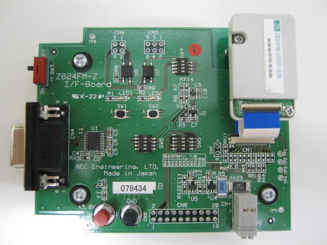
XQ3WRL
Aug 24, 2010Wireless data communication system
Equipment Class
DTS - Digital Transmission System