XUJX431TOOLCAUTOMOTIVE DIAGNOSIS COMPUTER
Launch Tech Co., Ltd.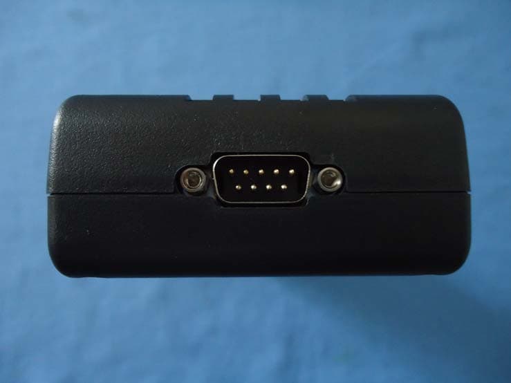
Click to zoom
Application Details
- Equipment Class
- DSS - Part 15 Spread Spectrum Transmitter
- Date of Grant
- Aug 30, 2011
- Application Purpose
- Original Equipment
- Date of Application
- Aug 30, 2011
- Equipment Note
- AUTOMOTIVE DIAGNOSIS COMPUTER
- Frequency Range
- 2402.00000000 - 2480.00000000
- Company
- Launch Tech Co., Ltd.
- Country
- China
Documents & Files
Document Text
Text extracted from the exhibit documents filed with the FCC. Open a document above to read the original.
Users Manual
V1.00.001 2011-04-07 LAUNCH X-431Tool User’s Manual i Trademark Information LAUNCH is a registered trademark of LAUNCH TECH. CO., LTD. (also called LAUNCH for short) in China and other countries. All other LAUNCH trademarks, service marks, domain names, logos, and company names referred to in this manual are either trademarks, registered trademarks, service marks, domain names, logos, company names of or are otherwise the property of LAUNCH or its affiliates. In countries where any of the LAUNCH trademarks, service marks, domain names, logos and company names are not registered, LAUNCH claims other rights associated with unregistered trademarks, service marks, domain names, logos, and company names. Other products or company names referred to in this manual may be trademarks of their respective owners. You may not use any trademark, service mark, domain name, logo, or company name of LAUNCH or any third party without permission from the owner of the applicable trademark, service mark, domain name, logo, or company name. You may contact LAUNCH by visiting Launch at http:// www. cnlaunch. com , or writing to LAUNCH TECH. CO., LTD.,Launch Industrial Park,North of Wuhe Avenue, Banxuegang, Bantian, Longgang, Shenzhen, Guangdong,P. R . C h i n a , to request written permission to use Materials on this manual for purposes or for all other questions relating to this manual. Copyright Information Copyright © 2011 by LAUNCH TECH. CO., LTD. All rights reserved. No part of this publication may be reproduced, stored in a retrieval system, or transmitted in any form or by any means, electronic, mechanical, photocopying, recording or otherwise, without the prior written permission of LAUNCH. The information contained herein is designed only for the use of this unit. LAUNCH is not responsible for any use of this information as applied to other units. Neither LAUNCH nor its affiliates shall be liable to the purchaser of this unit or third parties for damages, losses, costs, or expenses incurred by purchaser or third parties as a result of: accident, misuse, or abuse of this unit, or unauthorized modifications, repairs, or alterations to this unit, or failure to strictly comply with LAUNCH operating and maintenance instructions. LAUNCH shall not be liable for any damages or problems arising from the use of any options or any consumable products other than those designated as Original LAUNCH Products or LAUNCH Approved Products by LAUNCH. General Notice z Other product names used herein are for identification purposes only and may be trademarks of their respective owners. LAUNCH disclaims any and all rights in those marks. z There is a possibility that this unit is inapplicable to some of the vehicle models or systems listed in the diagnosis section due to different countries, areas, and/or years. Do not hesitate to contact LAUNCH if you come across such questions. We are to help you solve the problem as soon as possible. Disclaimer z To take full advantage of the unit, you should be familiar with the engine. z All information, illustrations, and specifications contained in this manual are based on the latest information available at the time of publication. The right is reserved to make change at any time without notice. LAUNCH X-431Tool User’s Manual ii Table of Contents Introduction.......................................................2 Features.........................................................2 Outline of X-431TOOL......................................3 Structure and explanations...............................4 Ports and Indicators.........................................5 Hardware Configuration...................................5 Printer Operation.............................................7 Mounting Paper...........................................7 Specifications..................................................8 First Use of X-431TOOL...................................9 Start-up......................................................9 Taskbar......................................................9 Input........................................................10 Control of App...........................................11 Help.........................................................11 Vehicle Diagnosis............................................12 Conditions for Test.........................................12 Select Diagnostic Connector...........................12 Diagnostic Socket Location.............................12 Connection...................................................12 Operation......................................................13 Entering Function Menu.............................13 Control module..........................................14 Resetting Maintain/oil Indicator.......................24 Setting Service Code.....................................25 OBDII Diagnostic function...........................25 Freeze Frame Data...................................25 Readiness Test.........................................26 Diagnostic Socket Description.........................26 Update of diagnostic software.........................27 User Registration.......................................27 Software Update.......................................28 Flow Chart of X-431TOOL Update for New User ....................................................................33 PDA function....................................................34 System information........................................ 36 User Information....................................... 36 About....................................................... 36 Tool.............................................................. 36 PIM.............................................................. 39 Memo...................................................... 39 Address.................................................... 41 Delete Address......................................... 42 To D o................................................…
Text truncated - open the document above for the full version.
Block Diagram
1 2 3 4 5 6 78 ABCD 8 7 6 5 4 3 2 1 D CBA Title Number Revision Size A2 Date: 22-Jul-2011 Sheet of File: D:\e\h eavy-du ty\h ec vy- du ty II \HEA VY-DUT Y 单刀继电器版 \HEA VY-DUT Y_S_RELAY 1.00 .00 0.dd b Drawn By: ARM Serial RAM Drive ResetCircuit RS232 BLUETOOTH Voltage Logic to ParallelSelect Circuit SelectCircuitCircuit RelaySwitchArray DB15 Connector DOUBLE CANSINGLE CAN Kline Positive Lline Kline Negative PWM&VPW DTSTDS 5V DC/DC 3V3 LDO Crystal INPUT VBAT LPC9107单片机 Transceiver Transceiver Transceiver Transceiver TransceiverTransceiver Logic Logic 24V Voltage regulator
Cover Letter(s)
SCS-F18: Project and Product Certification Representative Authorization Letter Page 1 of 2 Rev 2.0 2206 Ringwood Avenue San Jose, CA 95131 Tel: 408-526-1188 Fax: 408-526-1088 Email: [email protected] Project and Product Certification Representative Authorization Letter Revision History Reason for Amendment (current / obsolete) From To Approved Date Initial Release (current) 1.0 1.0 Revised wording (current) 1.0 2.0 SCS-F18: Project and Product Certification Representative Authorization Letter Page 2 of 2 Rev 2.0 Launch Tech Co., Ltd. August 11, 2011 To: SIEMIC, INC. 2206 Ringwood Avenue, San Jose, CA 95131 USA Dear Sir/Madam, Re: Project and Product Certification Representative Authorization Letter We, Launch Tech Co., Ltd. hereby authorize SIEMIC, INC. to act as a Certification Body for certifying for the following project(s): EUT: AUTOMOTIVE DIAGNOSIS COMPUTER N/N: X-431 TOOL C FCC ID: XUJX431TOOLC We affirm that between SIEMIC and Launch Tech Co., Ltd., any difference in understanding, including test plan, measurement methods, applicable standards and relevant procedures and processes have been resolved prior to commencement of testing activities. Name: Lihua WU Title: Certification Engineer Telephone: +86-075584528007 Fax No.: +86-075584528054 Launch Tech Co., Ltd. Launch Industrial Park, North Wuhe Avenue, Banxuegang Industrial Park, Longgang District, Shenzhen, China
Cover Letter(s)
Date:2011-8-11 To: Federal Communications Commission 7435 Oakland Mills Road Columbia, MD FCC ID:XUJX431TOOLC To Whom It May Concern: Launch Tech Co., Ltd. This letter is to ascertain that SCM Microsystems, Inc. Product AUTOMOTIVE DIAGNOSIS COMPUTER has been the units used for conducting FCC compliance testing, the DoC part will be tested by FCC recognized test lab. If you have any question or concerns, pls. contact us. Sincerely, Name: Lihua WU Title: Certification Engineer Telephone: +86-075584528007 Fax No.: +86-075584528054 Launch Tech Co., Ltd. Launch Industrial Park, North Wuhe Avenue, Banxuegang Industrial Park, Longgang District, Shenzhen, China
ID Label/Location Info
FCC ID: XUJX431TOOLC This device complies with Part 15 of the FCC Rules. Operation is subject to the following two conditions: (1) this device may not cause harmful interference, and (2) this device must accept any interference received, including interference that may cause undesired operation.
ID Label/Location Info
未命名 (823x407x24b jpeg)
Internal Photos
RF Antenna
Operational Description
Circuit Description X-431 TOOL C Power supply system (DC): The system power supply is provided by the OBD connector and converted to 5V as a main supply by DC/DC (U25). A branch of this 5V power supply is divided to supply the relay group and CAN bus transceiver. And meanwhile, the other branch is converted to 3.3V by LDO (U23) for the main CPU(U5) and extended logic. System clock configuration: The 8MHZ crystal oscillator provides the primary frequency clock. Memory system structure: LPC2368 is the CPU (U5) and with SRAM (U6) extended. The data transmits wireless via the Bluetooth module U1 5 to CPU U5 diagnostic box. The Bluetooth transmit frequency is 2402~2480MHz. Extended logistic structure: An extended CPLD (U7) fulfills the logistic extension to adapt the switches. Function module: The CAN bus transceiver (U2 1) performs the CAN BUS protocol among the vehicle ECUs. The SINGLE CAN bus transceiver (U20) communicates in single CAN BUS. The LOGIC LEVEL SHIFT converts the logic level to communicate. The PWM BUS UNIT links the special vehicle communication. The communication links can be switched by relay arrays which is driven by the relay drive unit U 8,U9,U10,U11,U12 and U13 according to the signal from the extended logic unit, so the shift fulfill various requirement of different car models and tests.
RF Exposure Info
RF EXPOSURE COMPLIANCE REQUIREMENT 1.1.Rules Part No. 15.247(b) 1.2.Limit The conducted output power limit specified in paragraph (b) of this section is based on the use of antennas with directional gains that do not exceed 6 dBi. Except as shown in paragraph (c) of this section, if transmitting antennas of directional gain greater than 6 dBi are used, the conducted output power from the intentional radiator shall be reduced below the stated values in paragraphs (b)(1). (b)(2). and (b)(3) of this section, as appropriate, by the amount in dB that the directional gain of the antenna exceeds 6 dBi. 1.3.Test Procedure EUT RF Exposure The Max Conducted Peak Output Power is 13.01dBm(19.99mW) in lowest channel (2.441GHz); The best case gain of the antenna is -2dBi. According to the formula. calculate the EIRP test result: EIRP= P x G = 19.99mW x 1 = 19.99mW ① SAR requirement: ② S= 60 / f(GHz) = 60/2.441 = 24.58mW ②; ① < ②. So the SAR report is not required.
Schematics
ABCD DCBA Title Number Revision Size A3 Date: 2-Jun-2011 Sheet of File: E:\TO OL_WIRE\ TO OL \ B OX\3.32 .00 0\TO OLWIRE _BOXV 3.32 .00 0.DD B Drawn By: X431WireToolBOX_V3X431WireToolBOX_V3.32_1.SCHX431WireToolBOX_V3X431WireToolBOX_V3.32_2.Sch X431WireToolBOX_V3X431WireToolBOX_V3.32_3.SCH X431WireToolBOX_V3X431WireToolBOX_V3.32_4.SCH X431WireToolBOX_V3X431WireToolBOX_V3.32_5.SCHX431WireToolBOX_V3X431WireToolBOX_V3.32_6.Sch 1 2 3 4 5 6 78 ABCD 8 7 6 5 4 3 2 1 D CBA Title Number Revision Size A3 Date: 2-Jun-2011 Sheet of File: E:\TO OL_WIRE\ TO OL\BOX\3.32 .00 0\TO OLWIRE _BOXV 3.32 .00 0.DD B Dr awn By: C1+ 1 V+ 2 C1- 3 C2+ 4 C2- 5 V- 6 T2OUT 7 R2IN 8 R2OUT 9 T2IN 10 T1IN 11 R1OUT 12 R1IN 13 T1OUT 14 GND 15 VCC 16 U14 SP3232E Y1 8MHz C630pF C730pF LCTRioPWMioVPWXMIT1BRCV1RCV2 RXDTXD C22 1uF C21 1uF C20 1uF btRXD mTXD1mRXD1 3V3 C100.1uFC110.1uFC120.1uFC130.1uF C140.1uF C150.1uF C160.1uF C170.1uF C180.1uF 3V3 btTXD 2 OF 4 V3.32.00 X431WireToolBOX_V3.32_1.SCH RXD0ACT_ISP RESET9107 P0.2 1 NC 2 P1.5/RST 3 VSS 4 P0.1 5 P1.0/TXD 6 P1.2/T0 7 P0.7/T1/CKO 8 P1.1/RXD 9 VDD 10 P0.5/CKI 11 P0.4 12 NC 13 P0.3 14 U16 P89LPC9107 R1810K 3V3 3V3 T6 P0.5 T7 P0.4 T5 RST mRXD2mTXD2 +5V 1 PAIR 2 GND 3 GND 4 RXD 5 RXD 6 LED 7 TXD 8 TXD 9 U15 BT_MODULE btTXDbtRXD 5V btPAIR 12 34 LED1BLUE 3V3 R17 220 spTEST Q103906 C230.1uF R16470 Ω R1510K C91uF P0.0/RD1/TXD3/SDA1 46 P0.1/TD1/RXD3/SCL1 47 P0.2/TXD0 98 P0.3/RXD0 99 P0.4/I2SRX_CLK/RD2/CAP2.0 81 P0.5/I2SRX_WS/TD2/CAP2.1 80 P0.6/I2SRX_SDA/SSEL1/MAT2.0 79 P0.7/I2STX_CLK/SCK1/MAT2.1 78 P0.8/I2STX_WS/MISO1/MAT2.2 77 P0.9/I2STX_SDA/MOSI1/MAT2.3 76 P0.10/TXD2/SDA2/MAT3.0 48 P0.11/RXD2/SCL2/MAT3.1 49 P0.15/TXD1/SCK0/SCK 62 P0.16/RXD1/SSEL0/SSEL 63 P0.17/CTS1/MISO0/MISO 61 P0.18/DCD1/MOSI0/MOSI 60 P0.19/DSR1/MCICLK/SDA1 59 P0.20/DTR1/MCICMD/SCL1 58 P0.21/RI1/MCIPWR/RD1 57 P0.22/RTS1/MCIDAT0/TD1 56 P0.23/AD0.0/I2SRX_CLK/CAP3.0 9 P0.24/AD0.1/I2SRX_WS/CAP3.1 8 P0.25/AD0.2/I2SRX_SDA/TXD3 7 P0.26/AD0.3/AOUT/RXD3 6 P0.27/SDA0 25 P0.28/SCL0 24 P0.29/USB_D+ 29 P0.30/USB_D- 30 P1.0/ENET_TXD0 95 P1.1/ENET_TXD1 94 P1.4/ENET_TX_EN 93 P1.8/ENET_CRS 92 P1.9/ENET_RXD0 91 P1.10/ENET_RXD1 90 P1.14/ENET_RX_ER 89 P1.15/ENET_REF_CLK 88 P1.16/ENET_MDC 87 P1.17/ENET_MDIO 86 P1.18/USB_UP_LED/PWM1.1/CAP1.0 32 P1.19/CAP1.1 33 P1.20/PWM1.2/SCK0 34 P1.21/PWM1.3/SSEL0 35 P1.22/MAT1.0 36 P1.23/PWM1.4/MISO0 37 P1.24/PWM1.5/MOSI0 38 P1.25/MAT1.1 39 P1.26/PWM1.6/CAP0.0 40 P1.27/CAP0.1 43 P1.28/PCAP1.0/MAT0.0 44 P1.29/PCAP1.1/MAT0.1 45 P1.30/VBUS/AD0.4 21 P1.31/SCK1/AD0.5 20 P2.0/PWM1.1/TXD1/TRACECLK 75 P2.1/PWM1.2/RXD1/PIPESTAT0 74 P2.2/PWM1.3/CTS1/PIPESTAT1 73 P2.3/PWM1.4/DCD1/PIPESTAT2 70 P2.4/PWM1.5/DSR1/TRACESYNC 69 P2.5/PWM1.6/DTR1/TRACEPKT0 68 P2.6/PCAP1.0/RI1/TRACEPKT1 67 P2.7/RD2/RTS1/TRACEPKT2 66 P2.8/TD2/TXD2/TRACEPKT3 65 P2.9/USB_CONNECT/RXD2/EXTIN0 64 P2.10/EINT0 53 P2.11/EINT1/MCIDAT1/I2STX_CLK 52 P2.12/EINT2/MCIDAT2/I2STX_WS 51 P2.13/EINT3/MCIDAT3/I2STX_SDA 50 P3.25/MAT0.0/PWM1.2 27 P3.26/MAT0.1/PWM1.3 26 P4.28/MAT2.0/TXD3 82 P4.29/MAT2.1/RXD3 85 TDO 1 TDI 2 TMS 3 TRST 4 TCK 5 RTCK 100 RSTOUT 14 RESET 17 XTAL1 22 XTAL2 23 RTCX1 16 RTCX2 18 VSS 15 VSS 31 VSS 41 VSS 55 VSS 72 VSS 97 VSS 83 VSSA 11 3.3V 28 3.3V 54 3.3V 71 3.3V 96 VDC_DC 13 VDC_DC 42 VDC_DC 84 VDDA 10 VREF 12 VBAT 19 U5 LPC2368 ACT_ISP T12 TDI T14 TDO T11 TMS T13 TCK TDI1TDO1TMS1TCK1nTRSTRTCK T15 TRST T16 RTCK T17 RST nRST canTXD1canRXD1canTXD2canRXD2TXD0RXD0xCANDATANSTBEN5790 extLED SERSRCLKRLCKSRCLR A0A1A2A3A4A5A6A7A8WRRD 3V3 btSTAT A9A10A11A12A13A14A15A16 D0D1D2D3D4D5D6D7 A11 1 A9 2 A8 3 A13 4 WE 5 CS2 6 A15 7 VDD 8 NC 9 A16 10 A14 11 A12 12 A7 13 A6 14 A5 15 A4 16 A3 17 A2 18 A1 19 A0 20 D0 21 D1 22 D2 23 GND 24 D3 25 D4 26 D5 27 D6 28 D7 29 CS1 30 A10 31 OE 32 U6 IS62WV1288BLL D0D1D2D3D4D5D6D7RDWR CS1 C80.1uF 3V3 T8 3V3 T9 3V3 3V33V3 T19 GND T20 GND GNDGND CE1 CS2 C190.1uF CE1 T1 TDI T2 TDO T3 TMS T4 TCK TDITDOTMSTCK IO 1 IO 2 IO 3 IO 4 IO 5 IO 6 IO 7 IO 8 VCCIO1 9 GNDIO 10 GNDINT 11 IO/GCLK0 12 VCCINT 13 IO/GCLK1 14 IO 15 IO 16 IO 17 IO 18 IO 19 IO 20 IO 21 TMS 22 TDI 23 TCK 24 TDO 25 IO 26 IO 27 IO 28 IO 29 IO 30 VCCIO1 31 GNDIO 32 IO 33 IO 34 IO 35 IO 36 IO 37 IO 38 IO 39 IO 40 IO 41 IO 42 IO/OE 43 IO/CLR 44 VCCIO1 45 GNDIO 46 IO 47 IO 48 IO 49 IO 50 IO 51 IO 52 IO 53 IO 54 IO 55 IO 56 IO 57 IO 58 VCCIO2 59 GNDIO 60 IO 61 IO/GCLK2 62 VCCINT 63 IO/GCLK3 64 GNDINT 65 IO 66 IO 67 IO 68 IO 69 IO 70 IO 71 IO 72 IO 73 IO 74 IO 75 IO 76 IO 77 IO 78 GNDIO 79 VCCIO2 80 IO 81 IO 82 IO 83 IO 84 IO 85 IO 86 IO 87 IO 88 IO 89 IO 90 IO 91 IO 92 GNDIO 93 VCCIO2 94 IO 95 IO 96 IO 97 IO 98 IO 99 IO 100 U7 EPM240 3V3 3V3 mRXD1mRXD2RXD0spTEST RLIO1RLIO2RLIO3RLIO4RLIO5RLIO6RLIO7RLIO8RLIO9RLIO10RLIO11RLIO12RLIO13RLIO14RLIO15RLIO16RLIO17RLIO18RLIO19RLIO20RLIO21RLIO22RLIO23RLIO24RLIO25RLIO26RLIO27RLIO28RLIO29RLIO30RLIO31RLIO32RLIO33RLIO34RLIO35RLIO36RLIO37RLIO38RLIO39RLIO40 RXY0RXY1RXY2RXY3RXY4RXY5RXY6RXY7RXY8RXY9RXY10RXY11RXY12RXY13TXY0TXY1TXY2TXY3TXY4TXY5TXY6TXY7TXY8TXY9TXY10TXY11TXY12TXY13RLCANRLSCANRLVORLLOGICRLPWMRLCANDATARLDTS4RLDTS8RLDTS11 TXD0mTXD1mTXD2extLEDxCANDATASERSRCLKRLCKSRCLR TXDRXDnRST T21T22T23T24 MCLR 1A 1 1Y 2 2A 3 2Y 4 3A 5 3Y 6 GND 7 4Y 8 4A 9 5Y 10 5A 11 6Y 12 6A 13 VCC 14 U8 SN7407D 1A 1 1Y 2 2A 3 2Y 4 3A 5 3Y 6 GND 7 4Y 8 4A 9 5Y 10 5A 11 6Y 12 6A 13 VCC 14 U9 SN7407D 1A 1 1Y 2 2A 3 2Y 4 3A 5 3Y 6 GND 7 4Y 8 4A 9 5Y 10 5A 11 6Y 12 6A 13 VCC 14 U10 SN7407D 1A 1 1Y 2 2A 3 2Y 4 3A 5 3Y 6 GND 7 4Y 8 4A 9 5Y 10 5A 11 6Y 12 6A 13 VCC 14 U11 SN7407D 1A 1 1Y 2 2A 3 2Y 4 3A 5 3Y 6 GND 7 4Y 8 4A 9 5Y 10 5A 11 6Y 12 6A 13 VCC 14 U12 SN7407D 1A 1 1Y 2 2A 3 2Y 4 3A 5 3Y 6 GND 7 4Y 8 4A 9 5Y 10 5A 11 6Y 12 6A 13 VCC 14 U13 SN7407D 3V33V33V33V33V33V3 RLIO1RLIO2RLIO3RLIO4RLIO5RLIO6RLIO7RLIO8RLIO9RLIO10RLIO11RLIO12RLIO13RLIO14RLIO15RLIO16RLIO17RLIO18RLIO19RLIO20RLIO21RLIO22RLIO23RLIO24RLIO25RLIO26RLIO27RLIO28RLIO29RLIO30RLIO31RLIO32RLIO33RLIO34RLIO35RLIO36RLIO37 Q52N3904 R14 220 SOE SOEbtPAIRspTEST MDO MCLK MCLRMCLKMDO ioLCTRL TXD0 RXD0 TXD RXD BOX_RXDBOX_TXD ACT_ISP 3V3 3V33V33V33V33V33V3 C10.1uF C20.1uF 3V3 R284.7K R28 No welding R40…
Text truncated - open the document above for the full version.
Test Report
Report No.: A001P110722008E-1 Page 1 of 36 FCC TEST REPORT for Launch Tech Co., Ltd. AUTOMOTIVE DIAGNOSIS COMPUTER Trade Name : LAUNCH Model No. : X-431 TOOL C FCC ID : XUJX431TOOLC Operating Frequency : 2402MHz - 2480MHz Antenna gain : -2dBi Applicant : Launch Tech Co., Ltd. Launch Industrial Park, North Wuhe Avenue, Banxuegang Industrial Park, Longgang District, Shenzhen, China Regulation : FCC Part 15.247 Subpart C Prepared by : Shenzhen AOV Testing Technology Co., Ltd. 2-6/F, No.5, Yuantou Lane , Tanglang, Taoyuan Street, Nanshan District, Shenzhen ,Guangdong, China Test Date : August 01-09, 2011 Date of Report : August 10, 2011 Report No.: A001P110722008E-1 Page 2 of 36 TABLE OF CONTENT Description Page Test Report Declaration 1. GENERAL INFORMATION..................................................................................................5 1.1 General Information....................................................................................................................5 1.2 Test Facility..................................................................................................................................5 1.3 Test Instrument Used.................................................................................................................6 2. POWERLINE CONDUCTED EMISSION TEST................................................................7 2.1. Test Standard..............................................................................................................................7 2.2. Limits............................................................................................................................................7 2.3. Test Procedure............................................................................................................................7 2.4. Test Result...................................................................................................................................7 3. MAXIMUM PEAK OUTPUT POWER...............................................................................10 3.1. Rules Part No............................................................................................................................10 3.2. Limits..........................................................................................................................................10 3.3. Test Procedure..........................................................................................................................10 3.4. Test Result.................................................................................................................................10 4. HOPPING CHANNEL SEPARATION AND BANDWIDTH...........................................11 4.1. Test Standard............................................................................................................................11 4.2. Limits..........................................................................................................................................11 4.3. Test Procedure..........................................................................................................................11 4.4. Test Result.................................................................................................................................11 5. NUMBER OF HOPPING FREQUENCY...........................................................................14 5.1. Test Standard............................................................................................................................14 5.2. Limits..........................................................................................................................................14 5.3. Test Procedure..........................................................................................................................14 5.4. Test Result.................................................................................................................................14 6. BAND EDGE.........................................................................................................................16 6.1. Rules Part No............................................................................................................................16 6.2. Limits..........................................................................................................................................17 6.3. Test Procedure..........................................................................................................................17 6.4. Test Result.................................................................................................................................17 7. DWELL TIME........................................................................................................................20 7.1. Rules Part No............................................................................................................................20 7.2. Limits..........................................................................................................................................20 7.3. Test Procedure..........................................................................................................................20 7.4. Test Result.................................................................................................................................20 8. RF ANTENNA CONDUCTED SPURIOUS EMISSIONS...............................................23 8.1. Rules Part No............................................................................................................................23 8.2. Limits..........................................................................................................................................23 8.3. Test Procedure................................................................................…
Text truncated - open the document above for the full version.
Test Setup Photos
Powerline conducted emission Radiated Emission Below 1G Above 1G
Contact Information
Applicant
Ivy Zhong(Manager)
Test Firm
Bontek Compliance Testing Laboratory LtdTony Wu
Technical Specifications
| # | Rule Parts | Frequency Range | Power Output |
|---|---|---|---|
| 1 | 15C | 2.40 GHz - 2.48 GHz | 19.99 mW |
Other Applications from Launch Tech Co., Ltd.
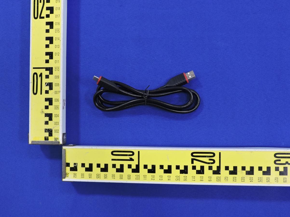
XUJOADDPD1303A
Sep 17, 2026Automotive Diagnostic Tool
Equipment Class
DTS - Digital Transmission System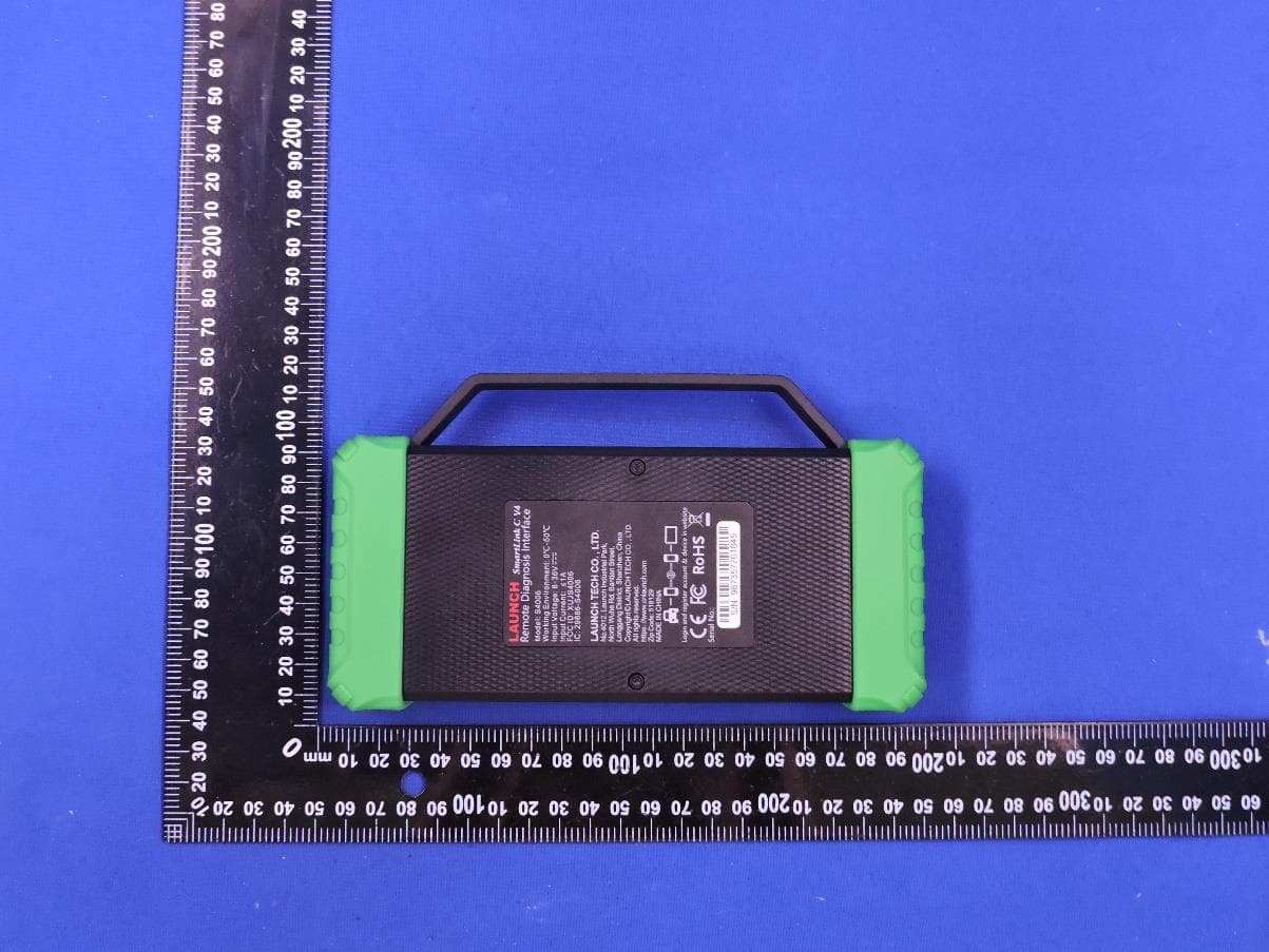
XUJS4006
Sep 04, 2026Remote Diagnosis Interface
Equipment Class
DTS - Digital Transmission SystemXUJEVT511S
Jul 09, 2026Battery Pack Airtightness Tester (High Voltage)
Equipment Class
DTS - Digital Transmission System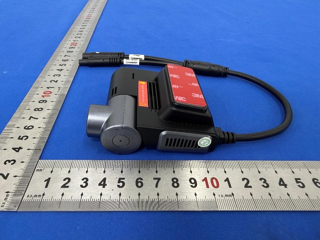
XUJG5201
Jun 26, 2026Car Sense Vision
Equipment Class
PCB - PCS Licensed Transmitter
XUJOADDPD1005A
Jun 05, 2026Automotive Diagnostic Tool
Equipment Class
NII - Unlicensed National Information Infrastructure TX