YM2FWTFIXED WIRELESS TERMINAL
Navitel Incorporated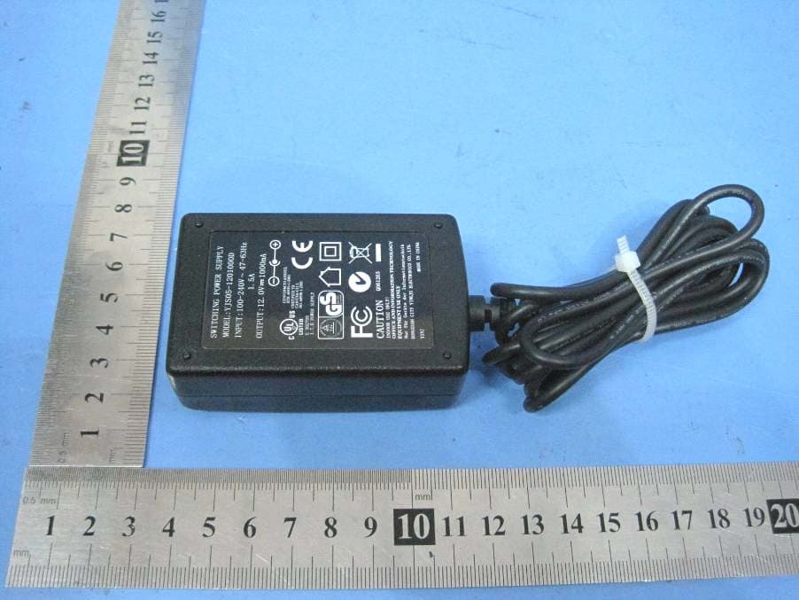
Click to zoom
Application Details
- Equipment Class
- PCB - PCS Licensed Transmitter
- Date of Grant
- Sep 09, 2010
- Application Purpose
- Original Equipment
- Date of Application
- Sep 09, 2010
- Equipment Note
- FIXED WIRELESS TERMINAL
- Frequency Range
- 1850.20000000 - 1909.80000000
- Company
- Navitel Incorporated
- Country
- United States
Documents & Files
Document Text
Text extracted from the exhibit documents filed with the FCC. Open a document above to read the original.
Users Manual
G4000RW Fixed Wireless Terminal User Guide Table of Contents ........................................................................................................................................ 1 1. Instructions 2. Main Features................................................................................................................................... 1 ......................................................................................................................................... 1 3. Installation .......................................................................................................................................... 2 4. Operation ....................................................................................................................... 2 5. Connectors and LED .................................................................................................................................... 4 6. Specifications ............................................................................................................................ 4 6.1. Power Supply .................................................................................................................. 4 6.2. GSM Specifications ............................................................................................................ 4 6.3. Physical Specifications .................................................................................................. 4 6.4. Environmental Specifications ........................................................................................................................ 5 Appendix: Packing List G4000RW Fixed Wireless Terminal G4000RW 1 1. Instructions Thanks for buying our GSM FWT (Fixed Wireless Terminal). GSM FWT is micro controller based equipment that can be interfaced to a standard telephone to transmit voice and data through GSM. 2. Main Features Connection with standard telephone for voice transmission. Connection with the Connection Box/PC for data transmission. GSM Industrial module with strong function and stable performance. High sensitivity antenna and low TX power. Easy operation and maintenance. Parameters programmable. 3. Installation 1) Select a suitable location for installation of the FWT that meets the following criteria. a. The location must be secure from theft. b. The location must be safe from falling or rising water. c. The location must be within the proper distance to a power source. d. The location must be such that the proper installation of an antenna is possible. 2) SIM card installation: The SIM card socket is built in. To install the SIM card, the user should remove the front cover, pull out the main board, and then insert the SIM card into the card socket. 3) Antenna installation: Connect the antenna to the SMA Antenna Connector, and then place it in the secure place. G4000RW Fixed Wireless Terminal G4000RW 2 4) Phone connection: Connect the telephone to the Telephone Interface on the FWT with the RJ11-RJ11 cable. 5) Connect the power supply to the Power Interface on the FWT. 6) Wait for the PWR (Power) LED to be alight. 7) If the LED is not alight, check the power source. Use a voltmeter to verify the DC output voltage is within the specification. If the power is correct but the LED’s not light, the FWT needs to be replaced. 8) Verify that you have simulated dial tone on telephone test set connected to the Telephone Interface on the FWT. If not, verify that the FWT is registered to the network by observing the LED. During the registration, the “SG” LED and the “PWR” LED will flash alternatively. Once the FWT successfully registers to the network, the “PWR” LED will keep alight and the “SG” LED will be alight in standby mode. If the FWT does not register, the SIM is not valid, the signal is too weak or the FWT needs to be replaced. 9) Make a test call and verify proper operation. 10) Secure the enclosure. 4. Operation Once the FWT successfully registers to the network, the “PWR” LED will keep alight and the “SG” LED will be alight in standby mode. Then the telephone connected to the FWT is ready for telephone service. 5. Connectors and LED G4000RW Fixed Wireless Terminal G4000RW 3 SG Power Interface A. Power Interface: Connected to the power supply (output: 12VDC±10%, 1000MA). B. PWR: The abbreviation of “power”. This is to indicate the power state. C. SG: The abbreviation of “signal”. This is to indicate the FWT registration state. D. Data:This port is used for updating its software by manufacturer,New version of the software will give users a new experience,Every user who wants to update the version ,should send the device to manufacturer to update it. E. SMA Antenna Connector: Connected to SMA antenna. F. Telephone Interface: Connected to standard telephone. SMA Antenna Connector PWR Data Telephone Interface G4000RW Fixed Wireless Terminal G4000RW 4 6. Specifications 6.1. Power Supply A. Input Voltage: 96-260VAC±10%, 50-60Hz B. Output Voltage: 12VDC±10% 1000mA C. Power Requirements: 300mA in talk mode (maximum) and 75mA in stand-by 6.2. GSM Specifications A. Supported Frequencies: 850/900/1800/1900 MHz B. Standards Compliance: GSM Phase 2/2+ a. Class 2 (2W @ 850/900MHz) b. Class2 (1W @ 1800/1900MHz) C. Signal Sensitivity: <-104dbm 6.3. Physical Specifications Fixed Wireless Terminal: A. Dimension: 110L×110W×26H B. Weight: 246g Connection Box: A. Dimension: 48L×44W×23H B. Weight: 34g 6.4. Environmental Specifications A. Ambient Temperature:-10~+50°C B. Relative Humidity: 0%~95% non-condensing G4000RW Fixed Wireless Terminal G4000RW 5 Appendix: Packing List G4000RW Fixed Wireless Terminal × 1 Power Adapter × 1 RJ11-RJ11 Cable × 1 Magnetic Base Antenna × 1 User Guide × 1 FCC RF Exposure Information and Statement: The Maximum Permission Exposure limit of USA (FCC) is 1mW/cm 2 . The EUT has also been tested against this MPE limit. The MPE value reported under this standard durin…
Text truncated - open the document above for the full version.
Block Diagram
CPU MT88L70AS Crystal Frequency=3.579MHz To Phone power LED Power mana g e r signal LED DC IN GSM RF Module 850 — 1900MHZ slic module SWR0822 Phone Port Block Diagram for Sl ic module SWR0822 Block Diagram fo r GSM RF module Fixed wireless Terminal G4000 Series FUNCTION ATI(HUIZHOU) TELEOMMUNCATIONS CO., LTD
Cover Letter(s)
Navitel Incorporated FCC ID: YM2FWT POWER OF ATTORNEY July 23, 2010 Federal Communications Commission Authorization and Evaluation Division 7435 Oakland Mills Road Columbia, MD 21046 To Whom It May Concern: We, the undersigned, hereby authorize Waltek Services (ShenZhen) Co., Ltd. (Philo Zhong) on our behalf, to apply to the Federal Communications Commission on our equipment. Any and all acts carried out by Waltek Services (ShenZhen) Co., Ltd. (Philo Zhong) on our behalf shall have the same effect as acts of our own. This authorization expires on July 22,2011 This is to advise that we are in full compliance with the Anti-Drug Abuse Act. We, Navitel Incorporated, are not subject to a denial of federal benefits pursuant to Section 5301 of the Anti- Drug Act of 1988, 21 USC853a, and no party to the application is subject to a denial of federal benefits pursuant to that section. Sincerely, Navitel Incorporated John Stage/Vice President Signature: ...................................................
External Photos
EUT - Components View EUT - Front View EUT - Back View Adapter - Front View Adapter - Back View
ID Label/Location Info
FCC ID Label This device complies with Part 15 of the FCC Rules. Operation is subject to the following two conditions:(1)this device may not cause harmful interference,and (2) this device must accept any interference received, including interference that may cause undesired operation. The Label must not be a stick-on paper. The Label on these products must be permanently affixed to the product and readily visible at the time of purchase and must last the expected lifetime of the equipment not be readily detachable. Proposed Label Location on EUT EUT Bottom View/proposed FCC Mark Location FCC ID: YM2FWT This device complies with Part 15 of the FCC Rules. Operation is subject to the following two conditions:(1)this device ma y not cause harmful interference,and (2) this device must accept any interference received, includin g interference that may cause undesired operation.
ID Label/Location Info
FCC ID Label Sample for Model: G4000 Series FWT FCC ID: YM2FWT This device complies with Part 15 of the FCC Rules. Operation is subject to the following two conditions:(1)this device may not cause harmful interference, and (2) this device must accept any interference received, including interference that may cause undesired operation.
Internal Photos
EUT – Open View EUT – PCB1 Front View EUT – PCB1 Back View EUT – PCB1 Module View EUT – PCB2 Front View EUT – PCB2 Back View Adapter – PCB Front View Adapter – PCB Back View
Operational Description
Circuit Description: The circuit mainly consists of two major components, including main board and Ringslic module. Please see the follow descriptions: 1. Main Board The main board consists of GSM module (SIM COM: SIM900), power devices (BM1430; LM317), CPU (SST 89V58D2), DTMF detecting devices (UT88L70),which crystal frequency is 3.579MHz,telephone port, power indicator (red LED) and signal Indicator (yellow LED). GSM module is for sending and receiving signal. Power devices are for voltage regulation and depressurizing. DTMF detecting device is for the dialing level identification. CPU is for central processing. Telephone port is for connection with telephone. 2. Ringslic module Ringslic module (SW0822) has the DC/DC voltage boosting function, ring current generating function, and provision of the 48V external power to telephone. 3. GSM RF module to achieve the voice,data communications(fax business) wireless access,provides the serial interface and CPU to link and data communications,voice interface and voice channel switching circuit connected and voice communications,with the SIM card interface. GSM RF module is a quad band module which supports GSM/GPRS. The baseband circuit is based on MTK(original ADI part) and RF circuit is based on Renensas. It works at quad bands, GSM850, EGSM900, DCS1800, and PCS1900 band. CPU clock is based on 26MHz crystal. The main IC include AD6720, AD6548, RPF08155B, HWXR874 and Combo Flash, etc.
Parts List/Tune Up Info
No.componentsspecificationquantity unitposition 10 RC0402JR-070RL MCR01MZPJ000 RC1005J000CS 0402WG J0000TCE RES MF 0R +/-5% 1/16W CH 0402 RO 6EA R1010 R1012 R1016 R1019 R2010 20 MCR01-MZS-J-102 RC0402JR-071KL RC1005J102CS 0402WG J0102TCE RES MF 1KR +/-5% 1/16W CH 0402 RO 9EA R1013 R2017 C2005 C2019 C2035 C1033 C1034 C1036 C1037 30 MCR01-MZS-J-152 RC0402JR-071K5L RC1005J152CS 0402WG J0152TCE RES MF 1.5KR +/-5% 1/16W CH 0402 RO 2 EA C2029 R2005 C1012 40 MCR01MZSJ222 RC0402JR-072K2L RC1005J222CS 0402WG J0222TCE RES MF 2.2KR +/-5% 1/16W CH 0402 RO 2 EA R2006 C1021 50 MCR01-MZS-J-103 RC0402JR-0710KL RC1005J103CS 0402WG J0103TCE RES MF 10KR +/-5% 1/16W CH 0402 RO 4EA R2009 R2014 R1030 R1031 60 MCR01-MZS-J-104 RC0402JR-07100KL RC1005J104CS 0402WG J0104TCE RES MF 100KR +/-5% 1/16W CH 0402 RO 4EA R2002 C1063 R3004 R2106 70 MCR01-MZS-J-106 RC0402 JR-0710ML RES MF 10MR +/-5% 1/16W CH 0402 RO 2 EA R2004 R2019 80 CM05CG1R0C50AH CC0402CRNPO9BN1R0 CL05C010CB5ANNC GRM1555C1H1R0CZ01D C0402C0G1R0C500NY CAP COG 1PF +/-0.25PF 50V CH0402 RO 1 EA R2018 C1005C0G1H2R2CT CC0402CRNPO9BN2R2 C1005C0G1H2R2CT GRM1555C1H2R2CZ01D C0402C0G2R2C500NY GRM1555C1H160JZ01D CAP COG 16PF +/-5% 50V CH0402 RO CM05CG100D50AH UMK105CG100DV-F CC0402JRNPO9BN100 GRM1555C1H100JZ01D C0402C0G100 J500NY CAP COG 10PF +/-5% 50V CH0402 RO CM05CG220J50AH CC0402JRNPO9BN220 CL05C220JB5NNNC GRM1555C1H220JZ01D C0402C0G220 J500NT C0402C0G220J500NT 120 CM05CG330J50AH CC0402JRNPO9BN330 CL05C330JB5NNNC GRM1555C1H330JZ01D C0402C0G330 J500NT CAP COG 33PF +/-5% 50V CH0402 RO 2 EA C1020 R2020 C1014 C1068 C2011110 CAP COG 22PF +/-5% 50V CH0402 RO 3EA 1008EA C2004 C2020 C2021 C2023 C2047 C2048 C2049 C2050 90 CAP COG 2.2PF +/-0.25PF 50V CH0402 RO 3 EA C1024 R2103 R1014 No.componentsspecificationquantity unitposition 130 CM05CG390J50AH CC0402JRNPO9BN390 CL05C390JB5NNNC GRM1555C1H390JZ01D C0402C0G390 J500NT CAP COG 39PF +/-5% 50V CH0402 RO 3 EA C1030 C1065 R3001 CM05CG470J50AH CC0402JRNPO9BN470 CL05C470JB5NNNC GRM1555C1H470JZ01D C0402C0G470 J500NT GRM1555C1H470JZ01D GRM1555C1H750JZ01D C0402C0G750J500NY CC0402JRNPO9BN750 CAP COG 75PF +/-5% 50V CH0402 RO CM05CG330J50AH CC0402JRNPO9BN330 CL05C330JB5NNNC GRM1555C1H330JZ01D C0402C0G330 J500NT CAP COG 33PF +/-5% 50V CH0402 RO C1005C0G1H101JT CM05CG101J50AH CC0402JRNPO9BN101 CL05C101JB5NNNC GRM1555C1H101JZ01D C0402C0G101 J500NT 170 CM05X7R102K50AH CC0402KRX7R9BB102 CL05B102KB5NNNC GRM155R71H102KA01D C0402X7R102K500NT CAP X7R 1NF +/-10% 50V CH0402 RO 2 EA C1043 C2038 C1005X7R1E103KT CAP X7R 10NF +/-10% 25V CH0402 RO CM05X7R103K16AH CC0402KRX7R7BB103 CL05B103KO5NNNC GRM155R71C103KA01D C0402X7R103K160NY CAP X7R 10NF +/-10% 16V CH0402 RO GRM155R71C104KA88D CL05B104K05NNNC C0402X7R104K160NY CAP X7R 100NF +/-10% 16V CH0402 RO CC0402KRX5R7BB104 CL05A104KO5NNNC EMK105BJ104KV-F C0402X5R104K160NY CAP X5R 100NF +/-10% CH0402 16V RO CM05X5R104K10AH C1005X5R1A104KT CC0402KRX5R6BB104 GRM155R61A104KA01D C0402X5R104K100NT C0402X5R104K100NY CAP X5R 100NF +/-10% 10V CH0402 RO 19011 EA C1032 C1038 C1039 C1064 C2001 C2002 C2003 C2036 C2053 C2101 C2102 1803 EA C1062 C1069 C2034 160 CAP COG 100PF +/-5% 50V CH0402 RO 1 EA C1066 140 CAP COG 47PF +/-5% 50V CH0402 RO 3 15012 EA C2017 C2018 C2022 C2024 C2025 C2027 C2028 C2031 C2032 C2040 C2041 C2052 EA C1001 C1015 C1061 No.componentsspecificationquantity unitposition CC0402KRX5R5BB224 C1005X5R0J224KT C0402X5R224K6R3NT CAP X5R 220NF +/-10% 6.3V CH0402 RO LMK105BJ224KV-F CAP CM1 220NF +/-10% 10V CH0402 RO GRM155R61A224KE19D CC0402KRX5R6BB224 CL05A224KP5NNNC C0402X5R224K100NY LMK105 B J224KV-F CAP X5R 220NF +/-10% 10V CH0402 RO JMK105BJ105KV-F CC0402KRX5R5BB105 CL05A105KQ5NNNC GRM155R60 J105KE19D CAP X5R 1UF +/-10% 6.3V CH0402 RO GRM155R60J105KE19D CAP CM1 1UF X5R 10% 6.3V CH0402 RO CC0603KRX5R6BB225 GRM188R61A225KE34D CAP X5R 2.2UF +/-10% 10V CH0603 RO C1608X5R0J225KT CM105X5R225K06AT CC0603KRX5R5BB225 JMK107BJ225KA-T CL10A225KQ8NNNC C1608X5R0 J225KT TAJA476M006RNJ CAP STA 47UF +/-20% 6.3V CH1206 RO 293D476X06R3A2TE3 CAP STA 47UF +/-20% 6.3V CH 3216-18 RO TAJA476K006RNJ CAP STA 47UF +/-10% 6.3V CH1206 RO 293D476X96R3A2TE3 CAP STA 47UF +/-10% 6.3V CH3216-18 RO GRM31CR60J226KE19L CL31A226KQHNNNE CAP X5R 22UF +/-10% 6.3V CH1206 RO LQG15HS3N3S02D IND HIGH 3.3NH +/-0.3NH CH0402 RO HK10053N3S-T电感3.3NH(0402) RO SDCL1005C3N3STDF MLK1005S3N3ST LQG15HS3N3S02D HK10053N3S-T IND HIGH 3.3NH +/-0.3NH CH0402 RO LQW15AN8N2G00D IND HIGH 8.2NH +/-2% CH0402 RO LQG15HS8N2J02D AQ1058N2J-T HK1005 8N2J-T SDWL1005C8N2JSTF AQ1058N2 J-T IND COIL 8.2NH +/-5% CH0402 RO SDCL1005C8N2JTDF LQG15HS8N2J02D HK1005 8N2J-T MLK1005S8N2DT000 IND HIGH 8.2NH +/-5% CH0402 RO IND HIGH 8.2NH +/-5% CH0402 RO C1010 C1011 2502EA C1010 C1011 2404EA C1017 C1018 C1019 L1001 2301 EA C1067 220 CAP X5R 2.2UF +/-10% 6.3V CH0603 RO 5EA C2008 C2014 C3003 C2012 C2051 2108EA C2006 C2007 C2009 C2010 C2013 C2015 C2037 C1022 2006EA C1035 C2026 C2043 C2044 C2045 C2046 No.componentsspecificationquantity unitposition LQG15HS5N6S02 IND HIGH 5.6NH +/-0.2NH CH0402 RO HK1005 5N6S-T IND HIGH 5.6NH +/-0.3NH CH0402 RO MLK1005S5N6DT000 IND HIGH 5.6NH +/-0.5NH CH0402 RO SDCL1005C5N6STDF HK1005 5N6S-T LQG15HS5N6S02 IND HIGH 5.6NH +/-0.3NH CH0402 RO ELJRF6N8JFB HK10056N8 J-T SDCL1005C6N8JTF HK10056N8J-T LQG15HS6N8 J02 HK1005 18NJ-T LQG15HS18NJ02 SDCL1005C18NJTDF HK1005 18NJ-T LQG15HS18N J02 MLK1005S56NJ电感56NH(0402) RO ELJRF56NJFB0402 56NH 电感 ±5% RO SDCL1005C56NJTDF LQG15HS56NJ02D HK1005 56NJ-T MLK1005S56N J IND HIGH 56NH +/-5% CH0402 RO B72590T0140L060B72590T0140L060 VARISTOR RO ICVL0518400V500FR B72590T0140L060 VARISTOR 14V CH0402 RO AVLC5S02050RES VAR CH 0402 RO SDV1005E180C300NPTFVARISTOR 18V 150PF CH0402 RO ESDA6V1-5W6-6/TRTVS-5 6.1V 100W SOT323-6L RO ESDA6V1-5W6(E)TVS RO 320 AD6720ABCZ-RL基带芯片 RO1 EA U20 330 TV00570002CDGB IC 128M+32M NOR+PSRAM FBGA RO 1 EA U202 340 AD6548BCPZ-RLRF TRANSCIEVER IC RO1 EA U1002 350 RPF08155B-TBIC RF PA 6X6X1.2 RO1 EA U1001 360 HWXR874-2前端模块(FEM) RO1 EA U1004 W-191-451 26MHZ 3.2*2.5MM CRYSTAL UNITES RO SQ3D02600L2LNA26MHZ3.2*2.5MM CRY…
Text truncated - open the document above for the full version.
RF Exposure Info
MAXIMUM PERMISSION EXPOSEURE Standard Applicable According to §1.1307(b)(1), system operating under the provisions of this section shall be operating in a manner that the public is not exposed to radio frequency energy level in excess limit for maximum permissible exposure. (a) Limits for Occupational / Controlled Exposure (b) Limits for General Population / Uncontrolled Exposure Frequency range (MHz) Electric Field Strength (E) (V/m) Magnetic Field Strength (H) (A/m) Power Density (S) (mW/cm2) Averaging Times | E |2, | H |2 or S (minutes) 0.3-3.0 614 1.63 (100)* 6 3.0-30 1842/f 4.89/f (900/f)* 6 30-300 61.4 0.163 1.0 6 300-1500 F/300 6 1500-100000 5 6 Frequency range (MHz) Electric Field Strength (E) (V/m) Magnetic Field Strength (H) (A/m) Power Density (S) (mW/cm2) Averaging Times | E |2, | H |2 or S (minutes) 0.3-1.34 614 1.63 (100)* 30 1.34-30 824/f 2.19/f (180/f)* 30 30-300 27.5 0.073 0.2 30 300-1500 F/1500 30 1500-100000 1 30 Note: f = frequency in MHz: * = Plane-wave equivalents power density MPE Calculation Method S =(P*G) / (4*∏*R 2 ) S = power density (in appropriate units, e.g., mw/cm 2 ) P = power input to the antenna (in appropriate units, e.g., mw) G = power gain of the antenna in the direction of interest relative to an isotropic radiator, the power gain factor is normally numeric gain. R = distance to the center of radiation of the antenna (in appropriate units, e.g., cm) MPE Calculation Result For GSM mode Maximum peak output power at antenna input terminal: 31.53(dBm) Maximum peak output power at antenna input terminal: 1422.3(mW) Prediction distance: 20 (cm) Prediction frequency: 824.2(MHz) Antenna gain (typical): 1 (dBi) Antenna gain (numeric): 1.2589 (numeric) The worst case is power density at prediction frequency at 20cm: 0.356 (mw/cm 2 ) MPE limit for general population exposure at prediction frequency: 1 (mw/cm 2 ) 0.356 (mw/cm 2 ) < 1 (mw/cm 2 ) Result: Compliant Maximum peak output power at antenna input terminal: 28.87(dBm) Maximum peak output power at antenna input terminal: 770.9(mW) Prediction distance: 20 (cm) Prediction frequency: 1850.2(MHz) Antenna gain (typical): 1 (dBi) Antenna gain (numeric): 1.2589 (numeric) The worst case is power density at prediction frequency at 20cm: 0.193 (mw/cm 2 ) MPE limit for general population exposure at prediction frequency: 1 (mw/cm 2 ) 0.193 (mw/cm 2 ) < 1 (mw/cm 2 ) Result: Compliant For GPRS mode Maximum peak output power at antenna input terminal: 31.49(dBm) Maximum peak output power at antenna input terminal: 1409.3(mW) Prediction distance: 20 (cm) Prediction frequency: 824.2 (MHz) Antenna gain (typical): 1 (dBi) Antenna gain (numeric): 1.2589 (numeric) The worst case is power density at prediction frequency at 20cm: 0.353 (mw/cm 2 ) MPE limit for general population exposure at prediction frequency: 1 (mw/cm 2 ) 0.353 (mw/cm 2 ) < 1 (mw/cm 2 ) Result: Compliant Maximum peak output power at antenna input terminal: 29.40(dBm) Maximum peak output power at antenna input terminal: 871.0(mW) Prediction distance: 20 (cm) Prediction frequency: 1850.2 (MHz) Antenna gain (typical): 1 (dBi) Antenna gain (numeric): 1.2589 (numeric) The worst case is power density at prediction frequency at 20cm: 0.218 (mw/cm 2 ) MPE limit for general population exposure at prediction frequency: 1 (mw/cm 2 ) 0.218 (mw/cm 2 ) < 1 (mw/cm 2 ) Result: Compliant
Schematics
日期 日期 日期 签 名 签 名 签 名 数量 数量 数量 更改单号 更改单号 更改单号 拟 制审 核标准化 等级标记 第 张 共 张 : : : 更改 标记 更改标记 更改标记 批 准 制图 描图 图幅 日期 签 名 旧底图总号 底图总号 (3) 格式 1 1 S 宝宝宝宝宝宝宝宝宝 C7010P C6910P +4V C34 33P C60.1u16V VP 1 VN 2 GS 3 VREF 4 INH 5 PWDN 6 X1 7 X2 8 VSS 9 OE 10 D0 11 D1 12 D2 13 D3 14 DV 15 EST 16 RT/GT 17 VDD 18 D1 MT88L70AS C2 0.1u160V +3.0V C4 20P C320P G1 3.579MHZ C50.1u16V R15 100K R11 56K R17330K C762200u6.3V C11 0.1u16V 12 XP2 C3033P C4910P 电 原 理 图 无无无无无无 F W - G4000RW-NSc FW-G4000RW-NSc.SCH R27 2K1% +12V 话话 C38 33P C7347u63V POWER IN 12VDC 1 2 3 4 5 6 XP4 UIM +12V R293K1% +4V R710K 王王王 2009-04-29 L1333uH A3 +3.0V FW-G4000RW-NSc.SCH C12 22u6.3V C48 10P C4010P C72 1u16V C2233P VH2RED LED VH1 YEL LED +4V R181.5K R191.5K VT2BC807 R310K R232.2K R242.2K R252.2K +3.0V RFL RC RSTK +4V +4V T2AT101 10:1 T1 AT103 1:1 C2833P C4710P C2933P C4410P C42 10P C43 10P C2433PC2533PC2633P C3633P C5310P C3910P C2133P C70.1u16V C4510P C2033P C4610P C2733P C8 0.1u16V RSTK SHK RFL RC C5610P100VC5710P100VC5810P100V C5933P100VC6033P100VC6133P100V VD101N4148 VD71N4148 VD8 1N4148 VD61N4148 VD9 1N4148 VD51N4148 UIM_IO UIM_RST UIM_CLK R610K XP5 C75 2200u16V RFL 5 SHK 6 RST 7 RC 4 TIP 2 RING 3 EXC 1 C+ 14 C_ 13 GND 11 VCC 10 VX 9 VR 8 N1 SWR0822 C6247u63V VIN 1 GND 3 EN 5 FB 4 VOUT 2 N2AMC2596-ADJP VD12SS14 R281.5K1% R2633K VD11SS14 C54 10P C3533P C100.1u16V V1.0 R16100K UIM_VDD UIM_VDD UIM_IO UIM_CLK UIM_RST R2022 R2122 R2222 UIM_CLK UIM_RST UIM_IO UIM_IO C5110P C5010P C5210P C3333P C3133PC3233P MICPMICN 1234 XP1MINUSB R5 10K VD41N4148 R410K C652200u16V C63 0.01u63V C64 0.01u63V C180.1u100V C19 0.1u100V C14 0.01u100V C15 0.01u100V C160.01u100VC170.01u100V L1 1mH L2 1mH R1256K DVDB4DB3DB2DB1 VT1 BC817 R1 10K R210K +3.0V D1_PWDN DB1 DB2 DB3 DB4 DV D1_PWDN RXD TXD RFL SHK RC RSTK C2333P C4110P SPKPSPKN DBGRX DBGTX L12120ohm LED0 VT3BC807 LED0 LED1 LED1 RESET RESET 123 XP3DEBUG DBGRXDBGTX RXDTXD C1 0.1u160V L10 120ohm L3120ohm L4 120ohm L5 120ohm L8 120ohm L7120ohmL6120ohm L9120ohm L111mH SPKPSPKN MICPMICN C742200u6.3V C90.1u16V C5510P C3733P Q1 A Q4 G Q2 B Q3 D C660.1u16V C6733P C6810P C71220u6.3V +3.0V NETLIGHT 1 VDD_VEXT 2 DISP_RST 3 DISP_D/C 4 DISP_CS 5 DISP_CLK 6 DISP_DATA 7 GND1 8 GPIO0 9 SIM_DATA 10 SIM_CLK 11 SIM_RST 12 SIM_VDD 13 SPK3N 14 SPK3P 15 SPK2N 16 SPK2P 17 MIC1P 18 MIC1N 19 SPK1N 20 SPK1P 21 MIC2P 22 MIC2N 23 AGND 24 GND2 25 LIGHT_MOS 26 SIM_PRESE 28 PWRKEY 29 KBR0 30 KBR1 31 KBR2 32 KBR3 33 KBR4 34 KBC0 35 KBC1 36 KBC2 37 KBC3 38 KBC4 39 GPIO1 40 DBG_TXD 41 DBG_RXD 42 GND3 44 RF_IN 45 GND4 46 GND5 47 GND6 48 GND7 49 GND8 50 GND9 51 ADC0 52 VBAT1 53 VBAT2 54 VBAT3 55 GND10 56 GND11 57 GND12 58 VCHG 59 BUZZER 60 RI 61 RTS 62 CTS 63 DSR 64 RXD 65 TXD 66 DTR 67 DCD 68 VRTC 27 A1 SIM340W C1310u10V VD31N4148 R1468K R13 47K R10 56K R956K R856K OUT 2 IN 3 GND 1 D2 SP809-31 VD1BZX84C-5V6VD2BZX84C-5V6 +3.0V C770.1u16V C780.1u16V *
Test Report
FCC TEST REPORT Page 1 of 64 FCC ID : YM2FWT Applicant : Navitel Incorporated Address of Applicant : 138 Mountain Brook Drive Canton,GA 30115 U.S.A Equipment Under Test (EUT) : Product description : Fixed Wireless Terminal Model No. : G4000 Series FWT Frequency Range : TX: 824.2 ~ 848.8 MHz / 1850.2 ~ 1909.8 MHz RX: 869.2 ~ 893.8 MHz / 1930.2 ~ 1989.8 MHz Standards : FCC 47 CFR PART 22 SUBPART H FCC 47 CFR PART 24 SUBPART E Date of Test : July 10~20, 2010 Tested By : Zero Zhou/ Reviewed By : Philo Zhong/ Test Result : PASS * PERPARED BY: Waltek Services (Shenzhen) Co., Ltd. 1/F, Fukangtai Building,West Baima Rd.,Songgang Street, Baoan District, Shenzhen 518105,China Tel :86-755-27553488 Fax: 86-755-27553868 The sample detailed above has been tested to compliance with FCC 47 CFR Part22 and Part24 of the FCC rules. The test results have been reviewed against the rules above and found to meet their essential requirements. Navitel Incorporated FCC ID: YM2FWT Page 2 of 64 2 Contents Page 1 COVER PAGE..........................................................................................................................................................1 2 CONTENTS ..............................................................................................................................................................2 3 TEST SUMMARY....................................................................................................................................................4 4 GENERAL INFORMATION..................................................................................................................................5 4.1 CLIENT INFORMATION............................................................................................................................................5 4.2 GENERAL DESCRIPTION OF E.U.T...........................................................................................................................5 4.3 DETAILS OF E.U.T. .................................................................................................................................................5 4.4 DESCRIPTION OF SUPPORT UNITS...........................................................................................................................5 4.5 STANDARDS APPLICABLE FOR TESTING..................................................................................................................5 4.6 TEST FACILITY........................................................................................................................................................5 4.7 TEST LOCATION......................................................................................................................................................6 5 EQUIPMENT USED DURING TEST ...................................................................................................................7 6 SPURIOUS RADIATION EMISSIONS TEST .....................................................................................................8 6.1 MEASUREMENT UNCERTAINTY...............................................................................................................................8 6.2 TEST PROCEDURE...................................................................................................................................................8 6.3 TEST SETUP............................................................................................................................................................9 6.4 SPECTRUM ANALYZER SETUP...............................................................................................................................10 6.5 CORRECTED AMPLITUDE & MARGIN CALCULATION............................................................................................10 6.6 SPURIOUS RADIATION EMISSIONS TEST RESULT...................................................................................................11 7 MAXIMUM PEAK OUTPUT POWER...............................................................................................................27 7.1 TEST PROCEDURE..................................................................................................................................................27 7.2 TEST RESULTS......................................................................................................................................................28 8 OCCUPIED BANDWIDTH ..................................................................................................................................37 8.1 TEST PROCEDURE.................................................................................................................................................37 8.2 TEST DATA............................................................................................................................................................37 9 SPURIOUS EMISSIONS AT ANTENNA TERMINALS ..................................................................................40 9.1 TEST PROCEDURE.................................................................................................................................................40 9.2 TEST DATA............................................................................................................................................................40 10 BAND EDGES ........................................................................................................................................................46 10.1 TEST PROCEDURE............................................................................................................................................46 10.2 TEST DATA......................................................................................................................................................46 11 FREQUENCY STABILITY ..............................…
Text truncated - open the document above for the full version.
Test Setup Photos
Radiated Emission Test View Below 1GHz Radiated Emission Test View Above 1GHz
Contact Information
Applicant
John Stage(Vice President)
Test Firm
Waltek Services(Shenzhen) Co., Ltd.Philo zhong
Technical Specifications
| # | Rule Parts | Frequency Range | Power Output | Emission | Tolerance |
|---|---|---|---|---|---|
| 2 | 24E | 1.85 GHz - 1.91 GHz | 870.00 mW | 261KGXW | 41 Hz |