YW5-JHPC1206906A9.7 INCH MID
Shenzhen Firstview Electronic Co. Ltd.
Click to zoom
Application Details
- Equipment Class
- JBC - Part 15 Class B Computing Device/Personal Computer
- Date of Grant
- Jun 20, 2012
- Application Purpose
- Original Equipment
- Date of Application
- Jun 20, 2012
- Equipment Note
- 9.7 INCH MID
- Country
- China
Documents & Files
Document Text
Text extracted from the exhibit documents filed with the FCC. Open a document above to read the original.
Users Manual
FederalCommunicationsCommission(FCC)Statement Thisdevicecomplieswithpart15oftheFCCRules.Operationissubjecttothefollowingtwoconditions:(1)Thisdevice maynotcauseharmfulinterference,and(2)thisdevicemustacceptanyinterferencereceived,includinginterferencethat maycauseundesiredoperation. Note:ThisequipmenthasbeentestedandfoundtocomplywiththelimitsforaClassBdigitaldevice,pursuanttopart15 oftheFCCRules.Theselimitsaredesignedtoprovidereasonableprotectionagainstharmfulinterferenceinaresidential installation.Thisequipmentgenerates,usesandcanradiateradiofrequencyenergyand,ifnotinstalledandusedin accordancewiththeinstructions,maycauseharmfulinterferencetoradiocommunications.However,thereisno guaranteethatinterferencewillnotoccurinaparticularinstallation.Ifthisequipmentdoescauseharmfulinterferenceto radioortelevisionreception,whichcanbedeterminedbyturningtheequipmentoffandon,theuserisencouragedtotry tocorrecttheinterferencebyoneormoreofthefollowingmeasures: Reorientorrelocatethereceivingantenna. Increasetheseparationbetweentheequipmentandreceiver. Connecttheequipmentintoanoutletonacircuitdifferentfromthattowhichthereceiverisconnected. Consultthedealeroranexperiencedradio/TVtechnicianforhelp. Warning:ChangesormodificationsmadetothisdevicenotexpresslyapprovedbyShenzhenFirstviewElectronicCo. Ltd.mayvoidtheFCCauthorizationtooperatethisdevice. Note:Themanufacturerisnotresponsibleforanyradioortvinterferencecausedbyunauthorizedmodificationstothis equipment.Suchmodificationscouldvoidtheuser’sauthoritytooperatetheequipment. Note: Thismanualincludessomeimportantsafetymethodandsomeinformationabouthowtousethe productcorrectlytoavoidtheunnecessarytroubles.Beforeyouusetheproduct,pleaserefertothe manualcarefully. ● Don’tputtheproductinhightemperature,humidamddustyenvironment ●Don’tputtheproductinthevehicles,whosewindowsareclosed. ●Don’tthrowandcrashtheproductstrongly.Don’tvibratetheTFTscreen,oritwillbebrokendownordisplays abnormally. ●Choosethesuitablevolume,turndownthevolumeorpoweroffifyoufeelsyrigmusarisedfromthehighvolume. ●Chargeinthefollowingcase: ● A 、 Theiconshowsnocharge. ● B 、 Theoperationsystemself-closing,shutdownafterrestarting-up. ● C 、 Noresponseoftheoperationicon. ● D 、 Showredinthetoprightcorner. ●Don’tstopabruptlyduringtheplayerformatting、uploadinganddownloading,orleadtotheerrorofsoftware. ●Asforthelossesofinternalstorageleadsbythedamage、maintainanceandotherreasons,noresponsibilitythis companywillbear,sopleaseuseaccordingtothemanual. ● Don’tremovethepackagewithoutpermission.Don’tcleantheproductsbyalcohol 、 thinningagentandBenzene scrubbingstuff. ● Don’tusetheproductsinthenon-electronicsareas(liketheaeroplane) ● Don’tusetheproductswhenyouaredrivingandwalking,ortrafficaccidentwillbearised. ● TheUSBonlycanbeusedtotransferdata. ※ Thiscompanyretaintherighttoimproveproducts,nonoticewillbereleasedwhenspecificationordesignis changed ※ (Nowaterproof) 【 Note 】 :Allthepicturesinthismanualisforyourreference!nonoticewillbereleasedwhen specificationorappearanceischanged! 1.Illustartionofappearanceandbutton 2.Firstusage 2.1batterymanagementandcharge 2.2ConnectthePC 3.OperationModel 3.1MainModeldescription 3.2Statusbardescribe 3.3Theusageoftouchscreen 3.4basicsetting 3.5soundandrealisticsettingring,informandscreenbrightness 3.6application 3.7privacy 3.8devicememory 3.9languageandkeyboard 3.10thedateandtime 3.11USBmodechoice 3.12APKinstaller(applicationinstallationtools) 3.13settings 4.Installation 4.1basicfunction 4.2internetsynchronization 4.3buttons 4.4labels 4.5filepath 4.6progressbar 5.Firmwareupgrade 5.1steps 5.2internetsynchronization 6.Help 7.Appendix:USBDeviceInstall N 1.Illustartionofappearanceandbutton 1.1Touchscreen 7Inchtouchscreen : toclick 、 dragandotheroperationwithinthetoucharea 1.2POWER Poweron:Pressthebuttonandtheplayershowthestart-upingpicturethenthemachineshowthemenu: Poweroff:PressthebuttonMENUfor5seconds,thesystemshows“Poweroff”,clickthe“PowerOff”toend systemoperation. Screenlock:Pressthebuttontolockorunlockthescreen 【Note】:1.Inthecaseoflowbattery,thesystemwillendautomatically 2:Afterimproperlyshutdown,ifyouwanttorestart-up,themachinewillscanandrepairdisk,inthecaseofthis thescreenwillshowtheprogressstrip. 1.3Returnbutton PressESCtoreturntheformeroperationforshorttime,themenutoforalongtime 1.4Menu Pressthebutton”M”topopuptherelevant“Menu”. 1.5Volume Press“+、-”toadjustthevolume. 1.6Headphoneinterface Standard3.5mmHeadphoneinterface 1.7Videosoutputinterface HDMIoutputinterface; 1.8TF-CARD TF-CARDSLOT : CONNECTT-FLASHTSTORAGECARD ; 1.9MiniUSB MiniUSBInterface:toconnectcomputertotransferthedata,chargeorconnectUdisk 1.10ResetKey Inthecaseofsoftwarecrash,bythinarticletopressRESETkey,themachinewillshutdown 【Note】:Itisn’trecommendedthatusetheRESETkeyoften,orthemachinesystemwillbe damaged. 2、Firstusage 2.1batterymanagementandcharge Whenyouusethemachineforthefirsttime,pleasesecurethatthebatteryisfull-charged: InsertthechargeoradaptertotheUSBinterface. Thefirstandsecondtimemustholdon2hours,lateryoucanhold Onforabout4hours. 【 Note 】: Standardcharge(input:AC110~240V50/60HzMax : 180MAoutput:DC5.0~5.5V/1.5A)needed,no DCchargeoffered,byUSBinterfacetocharge. Duringthecharge,thebatteryiconisrunning. Whenchargeend,thebatteryiconwillbegreenandstoprunning. Inordertoextendlifetime,itissuggestedthatrechargewhenlowbattery; 【Note】:1、Ifnousageforalongtime,pleaserechargewithinamonthtoavoiddamagetothemachine resultedfromtheexhaustionofbattery. 2 、 AfterPoweroff,insertthecharge,ifthemachineshoweslowbattery 、 charging,ashorttime neededbeforethebatterycansupportthemachinetostartup. 3 、 Ifthemachineneedtobechargedinastandardtime,itmustbeinsleepmode. 2.2ConnectPC ConnectthePCandthismachinebyUSBcable,thenthemachineshowsUSBhasbeenconnecting,choose loadingtotransferdata,ifnot,itischarging. EntertheloadingModel,youcansend、deletethefileintheplayerorthestoragecard. 3.OperationModel 3.1MainModeldescription Themodelafterturnonthemachine: Onthemainscreen,youcan: Managethesoftwareicononthemainscreen:theiconbecomesbiggerafterpres…
Text truncated - open the document above for the full version.
Block Diagram
55 44 33 22 11 D D C C B B A A Micro SD/TF CARD Earphone SPEAKER BATT LCD DCIN 3.7V-4.2VUSB0 OTG DEBUG JTAG*6 NANDFLASH 4CE KEY G-Sensor PMU AXP209 Interconnect Network,and Power Driven USB1 HOST CAMERA BGA 441PIN MPU 128MB X 4 DDR3 (512MB) MIC HDMI/1080P BLOCK MAINCHIP BLOCK A10 Crystal(24MHz)Crystal(32.768KHz) RTC TitleSize Document Number Rev Date: Sheet of MAINCHIP_PAD_DDR3 <V1.0> A3 21 6 Tuesday, February 07, 2012 TitleSize Document Number Rev Date: Sheet of MAINCHIP_PAD_DDR3 <V1.0> A3 21 6 Tuesday, February 07, 2012 TitleSize Document Number Rev Date: Sheet of MAINCHIP_PAD_DDR3 <V1.0> A3 21 6 Tuesday, February 07, 2012
Cover Letter(s)
ShenzhenFirstviewElectronicCo.Ltd. 3-4/F,BlockB,Huafeng1stTechnologyZone,BaoanMainRoad,BaoanDistrict,Shenzhen,China AGENCYAUTHORIZATIONLETTER FCCID:YW5-JHPC1206906ADate:June20,2012 FederalCommunicationsCommission AuthorizationandEvaluationDivision 7435OaklandMillsRoad Columbia,MD21046 Towhomitmayconcern: We,theundersigned,herebyauthorizeShenzhenCTLElectromagnetic TechnologyCo.,Ltd.(MR.TracyQi)onourbehalf,toapplytotheFederal CommunicationsCommissiononourequipment.Anyandallactscarriedout byShenzhenCTLElectromagneticTechnologyCo.,Ltd.(MR.TracyQi)on ourbehalfshallhavethesameeffectasactsofourown.Thisauthorization expiresonJune19,2013. ThisistoadvisethatweareinfullcompliancewiththeAnti-DrugAbuse Act.We,ShenzhenFirstviewElectronicCo.Ltd.arenotsubjecttoadenial offederalbenefitspursuanttoSection5301oftheAnti-DrugActof1988, 21USC853a,andnopartytotheapplicationissubjecttoadenialoffederal benefitspursuanttothatsection. Sincerely, QuYang/Manager Tel:+86-755-29081735 Fax:+86-755-29081715
External Photos
V1.0Page 18 of 21 ReportNo.:CTL120525489-WF 6 .E x t e r n a la n dI n t e r n a lP h o t o so ft h eE U T ExternalPhotos V1.0Page 19 of 21 ReportNo.:CTL120525489-WF
ID Label/Location Info
FCCIDLabelInformation 1.Labellocation: 2.FCCIDLabel: ShenzhenFirstviewElectronicCo.Ltd. Model:M906FCCID:YW5-JHPC1206906A ThisdevicecomplieswithPart15oftheFCCRules.Operation issubjecttothefollowingtwoconditions:(1)thisdevicemay notcauseharmfulinterference,and(2)thisdevicemustaccept anyinterferencereceived,includinginterferencethatmaycause undesiredoperation.
Operational Description
Working principle The MID 906 based on a powerful ARM cortex A8 core With 3D accelerator, PMIC (A10), 4*256MB DDR2, Movinand. Applications processor allows user-interactive software and display your product-specific graphical data on a high-quality, touch screen-enabled 9.7”LCD available as an add-on out product. PAD 1051 include many fetures, such as camera, G-sensor, Audio. External TF Card etc. The PMIC (Power management) is designed for use with the I.MX51 applications processor requiring a highly integrated, bi-directional power management IC and communications device. Features include: *Battery charging *12 adjustable output low dropouts (LCO) with internal and external pass devices *Two boost converters *Real-time clock and crystal oscillator circuitry *SPI/12C bus interface
Schematics
55 4 4 3 3 2 2 1 1 D D C C B B A A DC/DC3-1.2V-1.2ADC/DC2-1.25V-1.6ALDO3-2.80V-400mALDO2-3.00V-200mALDO1-1.3V-30mA Batterycharger/detect LDO4-1.25V-3.3V-200mA IPSOUT3.3V-5V-2A for CPURTC-VDD ACIN(5V)2ABAT(4.2V) AVCC AXP209 AP1231B 12ZRM SY7208 AP3031 EUP2571 EUP2584 AP3019 LCD BIAS LCD BL USB OTG Optional POWER TREE INTERFACE/HDMICSI0-IOCSI1-IO CSI(1V8) SY8008B DRAM-VCC SY8008B 1V23V3 POWER TREE AP1231B 28ZRM CSI0 V 5 C D V 8 . 2 C D 1000mA300mA A m 0 0 0 1 A m 0 0 3 RT9193-33PB HDMI USBVBUS( 5 V-900m A ) SY8008B 1000mA 1000mA 1V5 1V8 3V3 300mA Title v e R r e b m u N t n e m u c o D e z i S t e e h S : e t a D of MAINCHIP_PAD_DDR3 <V1.0> A3 4 16 Tuesday, February 07, 2012 Title v e R r e b m u N t n e m u c o D e z i S t e e h S : e t a D of MAINCHIP_PAD_DDR3 <V1.0> A3 4 16 Tuesday, February 07, 2012 Title v e R r e b m u N t n e m u c o D e z i S t e e h S : e t a D of MAINCHIP_PAD_DDR3 <V1.0> A3 4 16 Tuesday, February 07, 2012 55 44 33 22 11 D D C C B B A A CPU1 CPU1 Differential pairs Z0= 100 ohm Equilong BUSZ0= 100 ohm ND0 SDQS0 ND1 SDQS0_SDQS1 ND2 SDQS1_- ND3 SDQS2 ND4 SDQS2_ ND5 SDQS3SDQS3_ ND6 SDQ17 SDQM0 ND7 SDQM1SDQM2SDQM3 SCK_SCK SCKE0SA0SA1 NAND-VCC SA2SA3SA4SDQ0SDQ1SA5SDQ2SA6SDQ3SA7SDQ4SDQ5SA8SDQ6SA9SDQ7SA10SDQ8SDQ9SA11SDQ10SA12SDQ11SA13SDQ12SA14SBA0SDQ13SBA1SDQ14SDQ15SBA2SDQ16SWESCASSRASSDQ18SCS0SDQ20 GND SDQ21SDQ22SDQ23SRSTSDQ24SDQ25SDQ26SDQ27SDQ28SODT0SDQ29SZQSDQ30SDQ31SVREF0SVREF3SVREF1SVREF2SDQ19 SDQ[31:0] SA[12:0] SDQM[3:0] SVREF[3:0] SBA[2:0] ND[7:0] SDQS[3:0] NAND-VCC GND AGND NAND-VCC DLLVDD CSI0-VCC GND DRAM-VCCCPUVDDINTVDDVCC-3V3 CSI1-VCC AGND CSI0-D3 10 NCE1 15 CSI1-D0CSI0-D4 10 CSI1-D1CSI1-PCLKCSI0-D5 10 NDQS 15 CSI0-MCLK 10 CSI1-D2CSI0-D6 10 NCE0 15 CSI0-HSYNC 10 CSI1-D3CSI0-D7 10 NRE 15 CSI0-VSYNC 10 CSI1-D4NRB0 15 CSI0-D0 10 CSI1-D5CSI0-D1 10 CSI1-D6 NWP 15 CSI0-D2 10 CSI1-D7CSI1-MCLKNWE 15 NCE2 15 CSI1-HSYNCNALE 15 NRB1 15 NCE3 15 CSI0-PCLK 10 CSI1-VSYNCNCLE 15 SDQ[31:0] 14 SA[12:0] 14 SA14 14 SDQM[3:0] 14 SVREF[3:0] 14 SCS0 14 SCKE0 14 SBA[2:0] 14 SCK 14 SCK_ 14 SWE 14 SCAS 14 SRAS 14 SDQS0_ 14 SDQS1_ 14 SDQS2_ 14 SDQS3_ 14 SRST 14 SODT0 14 ND[7:0] 15 SDQS[3:0] 14 SA13 14 GPS-VCC-EN GPS-MOSI GPS-SCS GPS-SCLK TitleSize Document Number Rev Date: Sheet of MAINCHIP_PAD_DDR3 <V1.0> A3 516 Monday, February 06, 2012 TitleSize Document Number Rev Date: Sheet of MAINCHIP_PAD_DDR3 <V1.0> A3 516 Monday, February 06, 2012 TitleSize Document Number Rev Date: Sheet of MAINCHIP_PAD_DDR3 <V1.0> A3 516 Monday, February 06, 2012 DRAM NANDTS0/CSI0TS1/CSI1 BGA441-APP U1-1 DRAM NANDTS0/CSI0TS1/CSI1 BGA441-APP U1-1 SDQ0 AB4 SDQ1 AC7 SDQ2 AC4 SDQ3 AB8 SDQ4 AC8 SDQ5 AB5 SDQ6 AB7 SDQ7 AC3 SDQ8 AB2 SDQ9 Y1 SDQ10 AC2 SDQ11 Y2 SDQ12 AA1 SDQ13 AB3 SDQ14 W2 SDQ15 AC1 SDQ16 N1 SDQ17 T2 SDQ18 N2 SDQ19 U1 SDQ20 U2 SDQ21 P1 SDQ22 T1 SDQ23 M2 SDQ24 L1 SDQ25 H1 SDQ26 L2 SDQ27 H2 SDQ28 J1 SDQ29 M1 SDQ30 G2 SDQ31 K2 SVREF0 H3 SVREF1 H4 SVREF2 Y5 SVREF3 AA8 SDQS0 AB6 SDQS0# AC5 SDQS1 AB1 SDQS1# AA2 SDQS2 R1 SDQS2# P2 SDQS3 K1 SDQS3# J2 SDQM0 AC6 SDQM1 W1 SDQM2 R2 SDQM3 G1 SCK# V2 SCK V1 SCKE0 N3 SCKE1 J4 SA0 W4 SA1 R4 SA2 U4 SA3 M4 SA4 Y4 SA5 N4 SA6 V4 SA7 M3 SA8 AA3 SA9 P4 SA10 L3 SA11 W3 SA12 P3 SA13 Y3 SA14 R3 SBA0 K3 SBA1 L4 SBA2 K4 SWE T3 SCAS U3 SRAS T4 SCS0 V3 SCS1 AA4 SZQ AA7 SRST AA6 SDBG0 P8 SDBG1 R8 ADBG N8 NWE#/SPI0_MOSI/PC0 M23 NALE/SPI0_MISO/PC1 M22 NCLE/SPI0_CLK/PC2 L23 NCE1/PC3 L22 NCE0/PC4 K23 NRE#/PC5 K22 NRB0/SDC2_CMD/PC6 J23 NRB1/SDC2_CLK/PC7 J22 NDQ0/SDC2_D0/PC8 H23 NDQ1/SDC2_D1/PC9 H22 NDQ2/SDC2_D2/PC10 G23 NDQ3/SDC2_D3/PC11 G22 NDQ4/PC12 H21 NDQ5/PC13 H20 NDQ6/PC14 G21 NDQ7/PC15 G20 NWP/PC16 M21 NCE2/PC17 F23 NCE3/PC18 F22 NCE4/SPI2_CS0/PC19 L21 K21 NCE5/SPI2_CLK/PC20 NCE6/SPI2_MOSI/PC21 J21 NCE7/SPI2_MISO/PC22 J20 SPI0_CS0/PC23 G19 NDQS/PC24 F21 NAND_VCC0 H19 NAND_VCC1 J19 TS0_CLK/CSI0_PCLK/PE0 E23 TS0_ERR/CSI0_MCLK/PE1 E22 TS0_SYNC/CSI0_HSYNC/PE2 D23 TS0_DVLD/CSI0_VSYNC/PE3 D22 TS0_D0/CSI0_D0/PE4 C23 TS0_D1/CSI0_D1/PE5 C22 TS0_D2/CSI0_D2/PE6 B23 TS0_D3/CSI0_D3/PE7 B22 TS0_D4/CSI0_D4/PE8 A23 TS0_D5/CSI0_D5/PE9 A22 TS0_D6/CSI0_D6/PE10 B21 TS0_D7/CSI0_D7/PE11 A21 TS1_CLK/CSI1_PCLK/SDC1_CMD/PG0 F20 TS1_ERR/CSI1_MLCK/SDC1_CLK/PG1 E21 TS1_SYNC/CSI1_HSYNC/SDC1_D0/PG2 E20 TS1_DVLD/CSI1_VSYNC/SDC1_D1/PG3 D21 TS1_D0/CSI1_D0/SDC1_D2/CSI0_D8/PG4 D20 TS1_D1/CSI1_D1/SDC1_D3/CSI0_D9/PG5 C21 TS1_D2/CSI1_D2/UART3_TX/CSI0_D10/PG6 E19 TS1_D3/CSI1_D3/UART3_RX/CSI0_D11/PG7 C20 TS1_D4/CSI1_D4/UART3_RTS/CSI0_D12/PG8 D19 TS1_D5/CSI1_D5/UART3_CTS/CSI0_D13/PG9 C19 TS1_D6/CSI1_D6/UART4_TX/CSI0_D14/PG10 D18 TS1_D7/CSI1_D7/UART4_RX/CSI0_D15/PG11 C18 ODT0 AA5 ODT1 J3 R1 240R1% R0402 R1 240R1% R0402 BGA441-APP U1-2 BGA441-APP U1-2 VCC0_DRAM G5 VCC1_DRAM H5 VCC2_DRAM L5 VCC3_DRAM M5 VCC4_DRAM R5 VCC5_DRAM T5 VCC6_DRAM W5 VCC7_DRAM W6 VCC8_DRAM W7 VCC9_DRAM Y6 VDD0_DLL M8 VDD1_DLL N9 VDD2_DLL P9 VDD0_CPU H11 VDD1_CPU H12 VDD2_CPU H13 VDD3_CPU H14 VDD4_CPU J12 VDD5_CPU J13 VDD0_INT J15 VDD1_INT J16 VDD2_INT K9 VDD3_INT K10 VDD4_INT K15 VDD5_INT L8 VDD6_INT L9 VDD7_INT R9 VDD8_INT R10 VDD9_INT T8 VCC_CARD N19 VCC0_LVDS W12 VCC1_LVDS W13 VCC2_LVDS W14 VCC_CSI0 F19 VCC_CSI1 E18 VCC0 H8 VCC1 H9 VCC2 H10 VCC3 H15 VCC4 J8 VCC5 J9 VCC6 J10 VCC7 J14 GND0_DRAM G3 GND1_DRAM G4 GND2_DRAM J5 GND3_DRAM K5 GND4_DRAM N5 GND5_DRAM P5 GND6_DRAM U5 GND7_DRAM V5 GND8_DRAM Y7 GND9_DRAM Y8 GND0_DLL M9 GND1_DLL N10 GND2_DLL P10 GND0 J11 GND1 K11 GND2 K12 GND3 K13 GND4 L10 GND5 L11 GND6 L12 GND7 M10 GND8 M11 GND9 M12 GND10 M13 GND11 N11 GND12 N12 GND13 P11 GND14 P12 GND15 R11 GND16 R12 GND17 T11 GND18 T12 GND0_LVDS W9 GND1_LVDS W10 GND2_LVDS W11 55 44 33 22 11 D D C C B B A A CPU2 CPU2 GNDGNDHVP UVCCULVDDHPVCCINHPVCCHPLDM0DP0DM1DP1UVCCDM2 RTCVDD TVOUT0 DP2 X2 PLLVP X1Y1Y2 AVCC VRA1VRA2VRP GNDGNDGNDGNDGNDTVDACVCC LVDS0-VP0 LCD0-D0 LVDS0-VN0 LCD0-D1 LVDS0-VP1 LCD0-D2 LVDS0-VN1 LCD0-D3 LVDS0-VN2 LCD0-D5 LVDS0-VPC LCD0-D6 LVDS0-VNC LCD0-D7 LVDS0-VP3 LCD0-D8 LVDS0-VN3 LCD0-D9 LVDS0-VP2 LCD0-D4 AVCC ULVDD TVDACVCC PLLVP UVCC HVP HPVCCIN GND GND RTCVDD AGND GND DRAM-VCC INTVDD DRAM-VCC GND RESET 7,9 HPL 11 VRA1 9 LCD0-D16 TVOUT0 VCC-…
Text truncated - open the document above for the full version.
Test Report
Shenzhen CTL Electromagnetic Technology Co., Ltd. Tel: +86-755-89486194 Fax: +86-755-89486187 FCC PART 15 SUBPART B TEST REPORT FCC Part 15B Report Reference No......................: CTL120525489-WF Compiled by ( position+printed name+signature)..: File administrators Andy Zhang Name of the organization performing the tests ( position+printed name+signature)..: Test Engineer Nie Quan Approved by ( position+printed name+signature)..: Manager Tracy Qi Date of issue.....................................: June 20, 2012 Representative Laboratory Name.: Shenzhen CTL Electromagnetic Technology Co., Ltd. Address.............................................: Zone B, 4/F, Block 20, Guangqian Industrial Park, Longzhu Road, Nanshan, Shenzhen 518055 China. Test Firm..........................................: Bontek Compliance Testing Laboratory Ltd Address.............................................: 1/F, Block East H-3, OCT Eastern Ind. Zone, Qiaocheng East Road, Nanshan, Shenzhen, China Applicant’s name............................: Shenzhen Firstview Electronic Co. Ltd. Address.............................................: 3-4/F, Block B, Huafeng 1st Technology Zone, Baoan Main Road, Baoan District, Shenzhen, China Test specification: Standard ...........................................: FCC Part 15B: Unintentional Radiators TRF Originator ..................................: Shenzhen CTL Electromagnetic Technology Co., Ltd. Master TRF.......................................: Dated 2011-01 Shenzhen CTL Electromagnetic Technology Co., Ltd.. All rights reserved. This publication may be reproduced in whole or in part for non-commercial purposes as long as the Shenzhen CTL Electromagnetic Technology Co., Ltd. is acknowledged as copyright owner and source of the material. Shenzhen CTL Electromagnetic Technology Co., Ltd. takes no responsibility for and will not assume liability for damages resulting from the reader's interpretation of the reproduced material due to its placement and context. Test item description .................... : 9.7inch MID Trade Mark .......................................: / Model/Type reference.......................: M906 Listed Models M715, M716, M712, M723, M728, M677, M738, M928, M906, M1028, M805, M828, M816, M1007, M1018, M516, M1038 I/O Type of EUT................................: USB Port/ Earphone Port/ DC Input Port I/O Q’TY............................................: 1/ 1/ 1 Antenna Type..............................: Interior FCC ID.......................................: YW5-JHPC1206906A Result................................................: Positive V1.0 Page 2 of 21 Report No.: CTL120525489-WF T E S T R E P O R T Test Report No. : CTL120525489-WF June 20, 2012 ______________________________________________________________________________________________ Date of issue Equipment under Test : 9.7inch MID Model /Type : M906 Listed Models : M715, M716, M712, M723, M728, M677, M738, M928, M906, M1028, M805, M828, M816, M1007, M1018, M516, M1038 Applicant : Shenzhen Firstview Electronic Co. Ltd. Address : 3-4/F, Block B, Huafeng 1st Technology Zone, Baoan Main Road, Baoan District, Shenzhen, China Manufacturer Shenzhen Firstview Electronic Co. Ltd. Address 3-4/F, Block B, Huafeng 1st Technology Zone, Baoan Main Road, Baoan District, Shenzhen, China Test Result according to the standards on page 4: Positive The test report merely corresponds to the test sample. It is not permitted to copy extracts of these test result without the written permission of the test laboratory. V1.0 Page 3 of 21 Report No.: CTL120525489-WF Contents 1. TEST STANDARDS .................................................................. 3 2. SUMMARY............................................................................. 3 2.1. General Remarks 3 2.2. Equipment Under Test 3 2.3. Short description of the Equipment under Test (EUT) 3 2.4. EUT operation mode 3 2.5. EUT configuration 3 2.6. Related Submittal(s) / Grant (s) 3 2.7. Modifications 3 3. TEST ENVIRONMENT............................................................... 3 3.1. Address of the test laboratory 3 3.2. Test Facility 3 3.3. Environmental conditions 3 3.4. Configuration of Tested System 3 3.5. Statement of the measurement uncertainty 3 3.6. Equipments Used during the Test 3 3.7. Summary of Test Result 3 4. TEST CONDITIONS AND RESULTS ............................................. 3 4.1. Conducted Emissions Test 3 4.2. Radiated Emissions Test 3 5. TEST SETUP PHOTOS OF THE EUT ........................................... 3 6. EXTERNAL AND INTERNAL PHOTOS OF THE EUT ........................ 3 V1.0 Page 4 of 21 Report No.: CTL120525489-WF 1. TEST STANDARDS The tests were performed according to following standards: FCC Part 15B : Unintentional Radiators ANCI C63.4: 2003 V1.0 Page 5 of 21 Report No.: CTL120525489-WF 2. SUMMARY 2.1. General Remarks Date of receipt of test sample : June 05, 2012 Testing commenced on : June 06, 2012 Testing concluded on : June 15, 2012 2.2. Equipment Under Test Power supply system utilised Power supply voltage : ●120V / 60 Hz o 115V / 60Hz o 12 V DC o 24 V DC o Other (specified in blank below) 2.3. Short description of the Equipment under Test (EUT) The device is a 9.7inch MID. For more details, refer to the user’s manual of the EUT. Serial number: Prototype 2.4. EUT operation mode Test Mode: 1. The EUT has been tested under normal operating condition. 2. No test program used to control the EUT within testing. 3. EUT Function and Test Mode. The field strength of radiation emission was measured in the following position: EUT stand-up position (Y axis), lie-down position (X, Z axis). The following data show only with the worst case setup. The worst case of Y axis was reported. Based on client request, all normal using modes of the normal function were tested but only the worst test data of the worst mode is reported by this report. 2.5. EUT configuration The following peripheral devices and interface cables we…
Text truncated - open the document above for the full version.
Test Setup Photos
5 . T e s tS e t u pP h o t o so f t h eE U T
Contact Information
Applicant
Qu Yang(manager)
Test Firm
Bontek Compliance Testing Laboratory LtdTony Wu
Technical Specifications
| # | Rule Parts | Frequency Range | Power Output |
|---|---|---|---|
| 1 | 15B | - | - |
Other Applications from Shenzhen Firstview Electronic Co. Ltd.
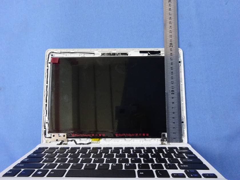
YW51166
Dec 05, 201511.6 inch net book
Equipment Class
JBC - Part 15 Class B Computing Device/Personal Computer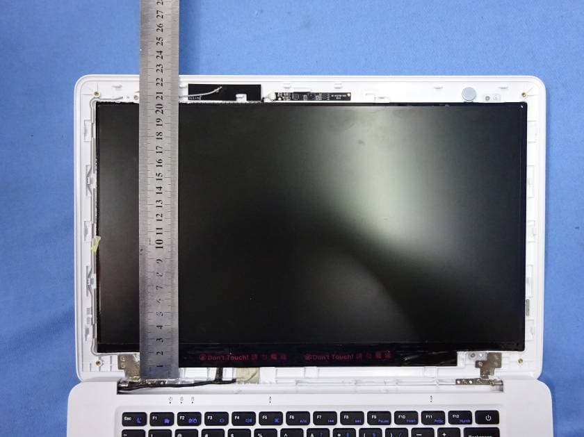
YW51401
Nov 23, 201514.1 inch net book
Equipment Class
DXX - Part 15 Low Power Communication Device Transmitter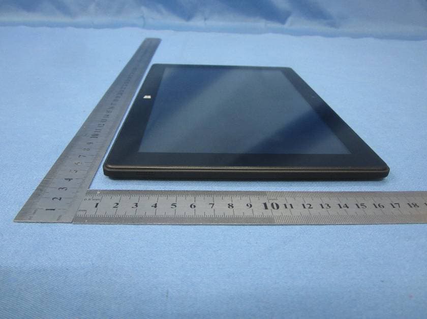
YW5VTA1005XBM32
Aug 18, 201510.1 inch tablet pc
Equipment Class
DTS - Digital Transmission SystemYW52AA95V01105
Nov 28, 201410.1 inch Tablet PC
Equipment Class
JBP - Part 15 Class B Computing Device PeripheralYW5VTA0801
Nov 20, 20148 inch Tablet PC
Equipment Class
DTS - Digital Transmission System