YZZGXV3500IP Video Codec
Grandstream Networks, Inc.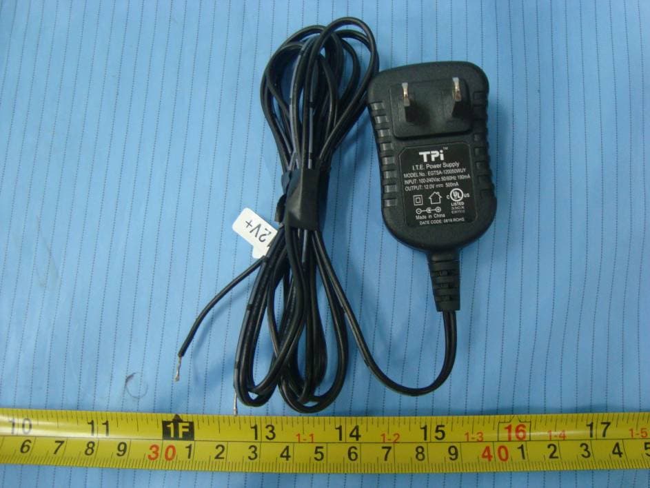
Click to zoom
Application Details
- Equipment Class
- JBP - Part 15 Class B Computing Device Peripheral
- Date of Grant
- May 25, 2011
- Application Purpose
- Original Equipment
- Date of Application
- May 25, 2011
- Equipment Note
- IP Video Codec
- Company
- Grandstream Networks, Inc.
- Country
- United States
Documents & Files
Document Text
Text extracted from the exhibit documents filed with the FCC. Open a document above to read the original.
Users Manual
GXV 3500 IP video Codec Quick Start Guide 1 PRECAUTIONS • Do not attempt to open, disassemble, or modify the device • Do not use a third party power adapter • Do not expose this device to temperatures outside the range of -10 C to +55 C • Do not expose the GXV3500 to environments outside of the following humidity range: 10-90% RH (non-condensing) PACKAGE CONTENTS GXV 3500 12V Power Supply 3.5mm to RCA audio/video cable QuickStart Guide 2 CONNECTING THE GXV3500 Refer to the illustration below when following the instructions on the next page. NOTE: Choose Option A if using the power supply. Or choose Option B if using a Power over Ethernet (PoE) switch. 3 Option A Step 1: Insert the power adapter into the 12V DC port on the GXV3500. Plug the other end of the adapter into an AC power outlet. Step 2: Plug an RJ45 Ethernet cable into the network port. Plug the other into a hub, switch or router. Option B Step 1: Plug an RJ45 Ethernet cable into the network port. Plug the other end into a Power over Ethernet (PoE) switch. 4 GXV3500 CONFIGURATION Configuring the GXV3500 using Microsoft Internet Explorer Step 1: Connect your PC and the GXV3500 to the same network. Step 2: Set the IP address of your PC to 192.168.1.X. set the Default Gateway of your PC to 255.255.255.0. 5 Step 3: Open Microsoft Internet Explorer on your PC. Type 192.168.1.168 in the address bar. Step 4: A pop-up window will appear with prompts for a user name and password. The default administrator user name and password are both set to “admin” at the default factory configuration. 6 Step 5: Once you log into the GXV3500’s web interface Internet Explorer will indicate that “This website wants to install to following add-on: ‘GSViewer.cab’ from Grandstream Networks, Inc.” Install this add-on by following the instructions. Step 6: Once the installation of GSViewX.cab completes you will see the web page shown in the screenshot on the next page. Click the play button to view the video feed. 7 Step 7: Click through the menu on the left hand side of the web UI for more advanced configuration parameters. Please download the user manual and FAQ for more detailed configuration instructions: http://www.grandstream.com/support/gxv_series_sur- veillance/gxv3500/documents/gxv3500_usermanual_english .pdf 8 GXV3500 SAMPLE CONNECTION DIAGRAM 9 FCC Warnings: Any Changes or modifications not expressly approved by the party responsible for compliance could void the user's authority to operate the equipment. This device complies with part 15 of the FCC Rules. Operation is subject to the following two conditions: (1) This device may not cause harmful interference, and (2) this device must accept any interference received, including interference that may cause undesired operation. This equipment has been tested and found to comply with the limits for a Class B digital device, pursuant to part 15 of the FCC Rules. These limits are designed to provide reasonable protection against harmful interference in a residential installation. This equipment generates uses and can radiate radio frequency energy and, if not installed and used in accordance with the instructions, may cause harmful interference to radio communications. However, there is no guarantee that interference will not occur in a particular installation. If this equipment does cause harmful interference to radio or television reception, which can be determined by turning the equipment off and on, the user is encouraged to try to correct the interference by one or more of the following measures: 10 ---Reorient or relocate the receiving antenna. ---Increase the separation between the equipment and receiver. ---Connect the equipment into an outlet on a circuit different from that to which the receiver is connected. ---Consult the dealer or an experienced radio/TV technician for help.
Cover Letter(s)
Company: Grandstream Networks, Inc. Address: 5F, Bldg #1, No.2 Kefa Rd., Science & Technology Park,ShenZhen,China Tel:0755-26014600-5503 Fax:0755-26014601 FCC Confidential Authorization Date: 2011-3-8 FEDERAL COMMUNICATIONS COMMISSIONS Authorization and Evaluation Division 7435 Oakland Mills Road Columbia, MD 21046 Confidentiality Request regarding application for certification of FCC ID: YZZGXV3500 Pursuant to Sections 0.457 and 0.459 of the Commission’s Rules, we hereby request confidential treatment of information accompanying this application as outlined below: • Detailed Circuit Schematics of EUT--- (Long term) Block Diagram--- (Long term) Circuit Description--- (Long term) The above materials contain trade secrets and proprietary information not customarily released to the public. The public disclosure of these materials may be harmful to the applicant and provide unjustified benefits to its competitors. The applicant understands that pursuant to Section 0.457 of the Rules, disclosure of this application and all accompanying documentation will not be made before the date of the Grant for this application. Sincerely Yours, Signature: Ning Wei Senior Director of Production
External Photos
EXHIBIT B - EUT EXTERNAL PHOTOGRAPHS EUT with AC/DC Adaptor View EUT –Front View EUT – Rear View EUT – Top View EUT – Bottom View EUT – AC/DC Adaptor View EUT –AC/DC Adaptor Label View
ID Label/Location Info
EXHIBIT A - FCC ID LABELING AND LOCATION FCC ID Label FCC ID Label Location The label shown shall be permanently affixed at a conspicuous location on the device and be readily visible to the user at the time purchase (Labeling requirements per 2.925) Label here
Internal Photos
EXHIBIT C - EUT INTERNAL PHOTOGRAPHS EUT – Cover off View EUT – Main Board Top View EUT – Main Board Bottom View EUT –MS-ME198407 Board Top View EUT –MS-ME198407 Board Bottom View
Operational Description
Description of Operation whole system, it has direct interface to on the board memory and all peripherals , so no glue logic is needed in system design. The system has one 1Gbit NAND flash which can be expanded to 16Gbit NAND flash. One 64MX16Bit DDR2 is used on the board, but it also can be expanded to 256MByte. The system also have some I/O port for the external multi-media applications, On network size, the to LAN, The MICIN and LING OUT for user to connect to tone arm and audio AMP, a CVBS connector lets user to be able to use TV for a bigger display, The IO connector are for the alarm in, alarm out and also for the RS485 control. 1 Interface The NAND flash in the system is mainly used for program and data storage, based on the application, the system May need to support up to 1GB NAND flash, the system s upports booting from 8-bit NAND devices (16-bit NAND devices are not supported),supports 4-bit ECC (1-bit ECC is not supported),supports NAND flash that requires chip select to stay low during the tR read time. Figure 6.1.1 below shows the interface between processor and NAND flash: h JESD79D-2A standard compliant DDR SDRAM devices and compliant Mobile DDR SDRAM devices . DDR2 SDRAM plays a key role in a DM365-based system. The DDR2 Memory Controller supports the following features: • JESD79D-2A standard compliant DDR2 SDRAM NAND_CS0 NAND_OE NAND_WE NAND_A1 NAND_A2 NAND_RB NAND_WP NAND_WAIT NAND_D[7:0] CS0# OE# WE# ALC CLE RB# WP# WAIT# IO[7:0] The TMS320DM365ZCE is the central controller of the GXV3500 system provide one 802.3 Ethernet RJ45 connection The TMS320DM365ZCE DDR2 Memory Controller is a dedicated interface to DDR2 / mDDR SDRAM. It supports 1.1 Interface between the TMS320DM365ZCE and NAND flash TMS320DM365ZCE 1.2 Interface between TMS320DM365ZCE and DDR2 SDRAM Figure 1.1 Signal connection between TMS320DM365ZCE and NAND flas NAND FLASH • Mobile DDR SDRAM • 256 MByte memory space • Data bus width 16 bits • Burst length: 8 • Burst type: sequential • 1 CS signal • Page sizes: 256, 512, 1024, and 2048 • SDRAM autoinitialization • Self-refresh mode • Power down mode • Prioritized refresh • Programmable refresh rate and backlog counter Main chip DM365 ‘s MAX operating frequency : 216MHz A[13:0] BA[2:0] CS# WE# CAS# RAS# CKE CLK CLK# LDM UDM LDSQ LDSQ# UDSQ UDSQ# DQ[15 ;0] DDR2 Memory DDR2_A[13:0] DDR2_BA[2:0] DDR2_CS# DDR2_WE# DDR2_CAS# DDR2_RAS# DDR2_CKE DDR2_CLK DDR2_CLK# DDR2_LDM DDR2_UDM DDR2_LDSQ DDR2_LDSQ# DDR2_UDSQ DDR2_UDSQ# DDR2DQ[15;0] TMS320 DM365ZCE Figure 1.2 Signal connection between TMS320DM365ZCE and DDR2 memory
Test Report
Note: This test report is prepared for the customer shown above and for the device described herein. It may not be duplicated or used in part without prior written consent from Bay Area Compliance Laboratories Corp. This report must not be used by the customer to claim product certification, approval, or endorsement by NVLAP*, or any agency of the Federal Government. * This report contains data that are not covered by the NVLAP accreditation and are marked with an asterisk “★” (Rev.2) FCC PART 15B MEASUREMENT AND TEST REPORT For Grandstream Networks, Inc. 5F, Bldg. #1, No. 2 Kefa Road, Science & Technology Park, Shenzhen, Guangdong, China FCC ID: YZZGXV3500 Report Type: Original Report Product Type: IP Video Codec Test Engineer: Grace Xi Report Number: RSZ11030802 Report Date: 2011-05-16 Reviewed By: Lisa Zhu EMC Engineer Prepared By: Bay Area Compliance Laboratories Corp. (Shenzhen) 6/F, the 3rd Phase of WanLi Industrial Building, ShiHua Road, FuTian Free Trade Zone Shenzhen, Guangdong, China Tel: +86-755-33320018 Fax: +86-755-33320008 Grandstream Networks, Inc. FCC ID: YZZGXV3500 Report No.: RSZ11030802 Page 2 of 22 FCC Part 15B Test Report TABLE OF CONTENTS GENERAL INFORMATION.......................................................................................................................................3 PRODUCT DESCRIPTION FOR EQUIPMENT UNDER TEST (EUT) .....................................................................................3 OBJECTIVE...................................................................................................................................................................3 RELATED SUBMITTAL(S)/GRANT(S).............................................................................................................................3 TEST METHODOLOGY..................................................................................................................................................3 TEST FACILITY.............................................................................................................................................................3 SYSTEM TEST CONFIGURATION ..........................................................................................................................5 JUSTIFICATION.............................................................................................................................................................5 EUT EXERCISE SOFTWARE..........................................................................................................................................5 EQUIPMENT MODIFICATIONS.......................................................................................................................................5 LOCAL SUPPORT EQUIPMENT LIST AND DETAILS........................................................................................................5 EXTERNAL I/O CABLE..................................................................................................................................................5 CONFIGURATION OF TEST SETUP.................................................................................................................................6 BLOCK DIAGRAM OF TEST SETUP................................................................................................................................7 SUMMARY OF TEST RESULTS ...............................................................................................................................9 FCC §15.107 – AC LINE CONDUCTED EMISSIONS ...........................................................................................10 MEASUREMENT UNCERTAINTY..................................................................................................................................10 EUT SETUP................................................................................................................................................................10 EMI TEST RECEIVER SETUP.......................................................................................................................................10 TEST PROCEDURE......................................................................................................................................................11 TEST EQUIPMENT LIST AND DETAILS.........................................................................................................................11 TEST RESULTS SUMMARY..........................................................................................................................................11 TEST DATA................................................................................................................................................................11 FCC §15.109 - RADIATED SPURIOUS EMISSIONS ............................................................................................16 MEASUREMENT UNCERTAINTY..................................................................................................................................16 EUT SETUP................................................................................................................................................................16 EMI TEST RECEIVER SETUP.......................................................................................................................................17 TEST PROCEDURE......................................................................................................................................................17 CORRECTED AMPLITUDE & MARGIN CALCULATION.................................................................................................17 TEST EQUIPMENT LIST AND DETAILS.........................................................................................................................18 TEST RESULTS SUMMARY..................................................…
Text truncated - open the document above for the full version.
Test Setup Photos
EXHIBIT D - TEST SETUP PHOTOGRAPHS AC Line Conducted Emissions - Front View (AC/DC Adapter) AC Line Conducted Emissions - Side View (AC/DC Adapter) AC Line Conducted Emissions - Front View (PoE) AC Line Conducted Emissions - Side View (PoE) Radiated Emissions - Front View (30-1000 MHz, AC/DC Adapter) Radiated Emissions - Rear View (30-1000 MHz, AC/DC Adapter) Radiated Emissions - Front View (Above 1 GHz, AC/DC Adapter) Radiated Emissions - Rear View (Above 1 GHz, AC/DC Adapter) Radiated Emissions - Front View (30-1000 MHz, POE) Radiated Emissions - Rear View (30-1000 MHz, POE) Radiated Emissions - Front View (Above 1 GHz, POE) Radiated Emissions - Rear View (Above 1 GHz, POE)
Contact Information
Applicant
Ning Wei
Test Firm
Bay Area Compliance Laboratory Corp. (Shenzhen)John Chan
Technical Specifications
| # | Rule Parts | Frequency Range | Power Output |
|---|---|---|---|
| 1 | 15B | - | - |
Other Applications from Grandstream Networks, Inc.
YZZGWN7712P
Sep 04, 2026Layer 2 Lite Managed Network PoE Switch
Equipment Class
JAD - Part 15 Class A Digital DeviceYZZGWN7801PC
Aug 27, 2026Enterprise Layer 2+ Compact Managed Switch
Equipment Class
JAD - Part 15 Class A Digital DeviceYZZGWN7823P
Aug 26, 2026Layer 3 Multi-Gigabit Network Switch
Equipment Class
JAD - Part 15 Class A Digital DeviceYZZGWN7703P
Aug 26, 202624 Unmanaged Gigabit Port and 2 SFP Port Switch with 24 PoE+
Equipment Class
JAD - Part 15 Class A Digital DeviceYZZGWN7673
Jul 29, 2026Dual-Band Wi-Fi 7 Access Point
Equipment Class
DTS - Digital Transmission System