Z2Z-7D03MID-WIFI PORTION
SHENZHEN LI RUI ELECTRONIC CO., LTD.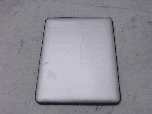
Click to zoom
Application Details
- Equipment Class
- DTS - Digital Transmission System
- Date of Grant
- Oct 05, 2011
- Application Purpose
- Original Equipment
- Date of Application
- Oct 05, 2011
- Equipment Note
- MID-WIFI PORTION
- Frequency Range
- 2412.00000000 - 2462.00000000
- Country
- China
Documents & Files
Document Text
Text extracted from the exhibit documents filed with the FCC. Open a document above to read the original.
Users Manual
i User’s Manual Manual Vision: 1.6 Release Date:August, 2011 ii User’s Notice Copyright of this manual belongs to the manufacturer. No part of this manual, including the products and software described in it may be reproduced, transmitted or translated into any language in any form or by any means without written permission of the manufacturer. This manual contains all information required for the utilization of this product to meet the user’s requirements. But it will change, correct at any time without notice. Manufacturer provides this manual “as is” without warranty of any kind, and will not be liable for any indirect, special, incidental or consequential damages (including damages for loss of profit, loss of business, loss of use of data, interruption of business and the like). Products and corporate names appearing in this manual may or may not be registered trademarks orcopyrights of their respective companies, and they are used only for identification or explanation and to the owner’s benefit, without intent to infringe. Package Contents PowerAdapter USB Cable OTG Cable Earphones Use r’s Manual Warranty Card iii Safety Instruction Operate the product according to the correct installation steps and with great care to make sure safety and comfort using experience. Please refer to the following safety instruction guide to avoid danger of electric shock or fire. Abide by the previous safety instruction guide to use and maintain the product and the hard disk to make sure of safe operating environment. Please follow the instruction manual fo roperation guide. The appropriate operating temperature ranges from 0 °C–35 °C (32 °F–95 °F). The operation humidity for this product is 5% to 80% RH. To avoid high temperature, please DO NOT overload the maximum power of the external power supply while the system is consuming high voltage. Be aware of the maximum temperature allowance of the power supply. See to it that the product is not working near the water. Always unplug power cable and other hardware cables from the system before cleaning. Apply only dry cloth forcleansing the product. Make sure that there is no heat source nearby when the product is working. iv Make sure that the thermal louverof the product is not blocked. Make sure to remove the powe rplug from the product when there is a thunder storm. Please remove the powe rplug from the product when you are not going to use the product for a long time. Make sure to set up o ruse the product on a stable surface. Make sure not to drop the product o rstrike it by any means. Make sure not to move the product when the device is charging power. Make sure not to step on the powe rcables and othercables or rest anything upon them. Please contact qualified technician fo rmaintenance orrepair. Use only accessories and parts that are made by the qualified manufacturer. -1- CHAPTER 1: BRIEF INTRODUCTION ................................................................. ‐2‐ 1.1 P RODUCTOVERVIEW .................................................................................... ‐2‐ 1.2 B UTTONS&CONNECTORS ........................................................................... ‐3‐ CHAPTER 2: PREPARATION BEFORE USING THE PRODUCT ................... ‐4‐ 2.1H OW TO POWER ON THE DEVICE .................................................................. ‐4‐ 2.2H OW TO POWER OFF THE DEVICE ................................................................. ‐5‐ 2.3 H OW TO CONNECT THE DEVICE TOPCORNOTEBOOK .............................. ‐5‐ 2.4 H OW TO USETFCARD .................................................................................. ‐6‐ 2.5 B ATTERYMANAGEMENT ANDCHARGE ........................................................ ‐6‐ 2.6 U SER’SINTERFACE ....................................................................................... ‐7‐ 2.7F UNCTIONLIST .............................................................................................. ‐9‐ CHAPTER 3 OPERATION GUIDE ....................................................................... ‐11‐ 3.1L ANGUAGE&KEYBOARDSETTINGS ......................................................... ‐11‐ 3.2W I-FISETTINGS ........................................................................................... ‐14‐ 3.3S TATICIPADDRESS SETTINGS AND CONNECTION ..................................... ‐21‐ 3.4USB HOST F UNCTION ............................................................................... ‐27‐ 3.5APKI NSTALLER .......................................................................................... ‐32‐ 3.6E XPLORER ................................................................................................... ‐36‐ 3.7 S OUN DRECORDER ...................................................................................... ‐39‐ 3.8 B ROWSER .................................................................................................... ‐41‐ 3.9 A NDROIDMARKET ....................................................................................... ‐44‐ CHAPTER4: HARDWARE CONFIGURATION .............................................. ‐51‐ Chapter 1: Brief Introduction TABLE OF CONTENT -2- 1.1 Product Overview OTG connector Volume- Power button Menu Button Escape TF card reader Speaker MIC Earphone Power connector Volume+ Camera USB connector Option Menu -3- 1.2 Buttons & Connectors NameFunction Power button Press for a long time to power on/off; Press for a short time to lock the screen or wake up the screen Volume + Press to increase the volume Volume - Press to decrease the volume Escape Escape: Press to return to upper menu Option Menu Option Menu: Press to view optional menu items of application Main menu Press to return to desktop; Press for a short time also to pop up relative menu Speaker Speaker output MIC Microphone for sound recording Earphone 3.5’’ earphone connector Power connector 2.5 mm DC5V/2A battery charging connector TF card reader External TF …
Text truncated - open the document above for the full version.
Cover Letter(s)
SHENZHEN LI RUI ELECTRONIC CO., LTD. FCC ID: Z2Z-7D03 POWER OF ATTORNEY September 26, 2011 Federal Communications Commission Authorization and Evaluation Division 7435 Oakland Mills Road Columbia, MD 21046 To Whom It May Concern: We, SHENZHEN LI RUI ELECTRONIC CO., LTD., hereby authorizeMost Technology Service Co., Ltd.(Terry YANG/ Manager) on our behalf, to apply to the Federal Communications Commission on our equipment. Any and all acts carried out byMost Technology Service Co., Ltd.(Terry YANG/ Manager) on our behalf shall have the same effect as acts of our own. This authorization expires onOctober 30, 2011. This is to advise that we are in full compliance with the Anti-Drug Abuse Act. We, SHENZHEN LI RUI ELECTRONIC CO., LTD. are not subject to a denial of federal benefits pursuant to Section 5301 of the Anti-Drug Act of 1988, 21 USC853a, and no party to the application is subject to a denial of federal benefits pursuant to that section. Li Fugang (Manager) SHENZHEN LI RUI ELECTRONIC CO., LTD. September 26, 2011
External Photos
FRONT VIEW OF SAMPLE BACK VIEW OF SAMPLE LEFT VIEW OF SAMPLE RIGHT VIEW OF SAMPLE TOP VIEW OF SAMPLE BOTTOM VIEW OF SAMPLE PHOTO OF POWER SUPPLY -MODEL 1 PHOTO OF POWER SUPPLY -MODEL 2 PHOTO OF THE ENTIRE SAMPLE
Internal Photos
INTERNAL PHOTO OF SAMPLE – 1 INTERNAL PHOTO OF SAMPLE -2 INTERNAL PHOTO OF SAMPLE -3 INTERNAL PHOTO OF SAMPLE -4 INTERNAL PHOTO OF SAMPLE -5 INTERNAL PHOTO OF SAMPLE -6 INTERNAL PHOTO OF SAMPLE -7 INTERNAL PHOTO OF SAMPLE -8 INTERNAL PHOTO OF SAMPLE -9 INTERNAL PHOTO OF POWER SUPPLY-1 INTERNAL PHOTO OF POWER SUPPLY-2
Operational Description
Buletooth Operating Description ProductMID Buletooth Function Frequency Range2400-2480 MHz ModulationFHSS Channel Number79 Channel Spacing1 MHz WLAN Operating Description ProductMID WLAN Function Frequency Range2412MHz – 2462MHz Modulation Technique IEEE 802.11b mode: DSSS (1, 2, 5.5 and 11 Mpbs) IEEE 802.11g mode: OFDM (6, 9, 12, 18, 24, 36, 48 and 54 Mpbs) IEEE 802.11n Standard-20 MHz Channel mode: OFDM(6.5, 13, 19.5, 26, 39, 52, 58.5, 65.0Mbps) Channel Number11 Channel Spacing5 MHz Max. Power12.69 dBm
RF Exposure Info
Maximum Permissible Exposure (MPE) Estimation 1. Limits and Guidelines on Exposure to Electromagnetic Fields General population/uncontrolled exposure apply in situations is which the general public may be exposed, or in which persons that are exposed as a consequenceof their employment may not be fully aware of the potential for exposure or can not exercise control over their exposure. The exposure levels can be expressed in terms of power density, electric field strength, or magnetic field strength, as averaged over 30 minutes for the general public and 6 minutes for trained personnel. The exposure criterion is frequency dependent, and a chart covering the range from 3 kHz to 100 GHz can be found in NCRP No.86 (references IEEE C95.1-1999). Below are the limits. Limits for Occupational/Controlled Exposure Frequency Range (MHz) Electric Field Strength (E) (V/m) Magnetic Field Strength (H) (A/m) Power Density (S) (mW/cm2) 0.3-3.0 3.0-30 30-300 300-1500 15,00-100,000 614 1842/f 61.4 -- -- 16.3/f 16.3/f 0.163 -- -- (100)* (900/f2)* 1.0 f/300 5 Limits for General Population/Uncontrolled Exposure Frequency Range (MHz) Electric Field Strength (E) (V/m) Magnetic Field Strength (H) (A/m) Power Density (S) (mW/cm2) 0.3-1.34 1.34-30.0 30-300 300-1500 15,00-100,000 614 824/f 27.5 -- -- 1.63 2.19/f 0.073 -- -- (100)* (180/f2)* 0.2 f/1500 1 Power density S [mW/cm2] for controlled area at 2441 MHz, S= 5 Power density S [mW/cm2] for uncontrolled area at 2441 MHz S= 1 Reference levels are provided for exposure assessment to determine whether the basic restrictions on exposure of humans to electromagnetic fields are exceeded. The basic restrictions on exposure to electromagnetic fields are based directly on established health effectsand biological considerations. 2. Prediction of the Exposure to Electromagnetic Fields Calculations can be made on a site by site basis toensure the power density is below the limits given above, or guidelines can be done beforehand to ensure the minimum distances from the antenna is maintained through the site planning. The calculations are based on FCC OET 65 Appendix B. 3. Calculation method of the Safe Distance Below method describes a theoretical approach to calculate possible exposure to electromagnetic radiation around a base station transceiver antenna. Precise statements are basically only possible either with measurements or complex calculations considering the complexity of the environment (e.g. soil conditions, near buildings and other obstacles) which causes reflections, scattering of electromagnetic fields. The maximum output power (given in EIRP) of a base station is usually limited by license conditions of the network operator. A rough estimation of the expected exposure in power flux density on a given point can be made with the following equation. The calculations are based on FCC OET 65 Appendix B. Whereas: S= Power Density P = Maximum output power in W of the site G numeric = Numeric gain of the antenna relative to isotropic antenna R = distance between the antenna and the point of exposure in meters 4. Test Result 435.5 MHz Power at antenna connector: 11.72dBm (11.49mW) Antenna gain: 1.8 dB (Numeric gain: 1.51) Predication Distance: 10 cm Predication Frequency: 2437MHz S= (11.49*1.51)/ (4*10*10*3.14) = 0.0138 (mW/cm 2 ) SO, Power Density at Predication Frequency and Predication Distance: 0.0138(mW/cm 2 ) Limit for General Population/Uncontrolled Exposure at the Predication Frequency: 1 (mW/cm 2 ) TEST RESULT: PASS
Schematics
Monday, June 27, 2011 AC/CHARGER LR7D01-29 MV1.4 1.4 Modify Date: Page Total: Page Num: File: Title: Create Date: REV: 深圳市力瑞电子有限公司 910mA IchargeAC=300X(2.5/Rset) 电池电压低于3.3V,PWR_EN为低, 作用:强制关机和电池低压不让机器开机。 BATTCharger DC input POWER ON CONTROL UNIT 2011-04-22 更改C5、C10为100UF/10V钽电容 封装为:3216L 2011-04-22 更改R18阻值,提高充电电流 2011-04-22 更改二极管型号,解决低电插拔充电器时自动重启的问题 2011-04-22 增加D21二极管,防止电池低电时插入充电器不能及时开机的问题 2011-05-04 更改R24 27K R34 47K 2011-05-23 更改R16、R22电阻阻值分别为:47K、10K 2011-05-23 删除R15、R17电阻,增加D22 IN5819 0805封装 删除R20、R21电阻 A B C D 54321 D C B A 12345 3 3 3 3 3,6,7 6,7 8 8 4 3,5 1 VOUT 2 GND 3 VDD U6 BL8506-33NRM R14100K Q2 SC70N 3904 + 1 2 C5 3216L 100uF/10V M4 MARK R32 R0402 4K7 D21 D0805 5819 R19 100K%1 12 D3 MPEG3030EP 1 1 2 2 3 3 4 4 5 5 SW1 PLAY 1 1 2 2 3 3 4 4 5 5 J1 DCJACK C9 C0402 105 R1960402R1M 1 VOUT 2 GND 3 VDD U52 S-80833CNMA-B8ST1G R126 0402R 100K M1 MARK Q4 SOT23A 3904 C14 C0805 106 R34 R0402 47K R30 R0402 10K R22 R0402 10K 1 3 2 D4 SOT23A BAT54C D22 D0805 IN5819 R197 0402R 1M - + 1 V+ 2 V- BT1 LI_3.7V 1 ACIN 2 USB 3 /CHG_S 4 /PGOOD 5 GND 6 ISETA 7 ISETU 8 /EN 9 TS 10 BATT 11 PAD U4 RT9502 R1950402R100K D6 SG-D1206 5819 R18 820R + 1 2 C10 3216L 100uF/10V R26 R0402 10K M5 MARK R23 R0402 4K7 12 D2 MPEG3030EP 1 VIN 2 GND 3 VOUT U3 ZEN056/ZEN132A230AC11 106 R24 R0402 27K ED9 ESD R37 NC R35 10K 1 3 2 Q17 3904 1 3 2 Q16 3904 R27 R0402 0R P2 ED8 ESD 1 2 C166 0805C 226 R1310K R11 100K%1 M2 MARK R36 1K%1 R16 R0402 47K C8 106 R1210K C554 105 R33 R0402 47K P1 D25 D0805 IN4148 M3 MARK R29 R0402560K C13 103 R145 0402R 1M C15 106 C7 100P R31 R0402 47K R28 10K 1 3 2 Q18 3904 C6 104 1 23 Q3 SOT23A WPM3401 1 3 2 D5 SOT23A BAT54C DC_5V VBUS BATT VCCIO DC_5V BATT DC_5V BATT VB DC_5V BATT DC_5V VB BATT DC_5VVBVBUS VCCIO BATT VCCIO DC_5V DC_DET CHG_OK BAT_DET PWR_KEY PWR_ON PWR_EN PLAY_VB PLAY_ON BAT_LOW RESET RESET BAT_LOW PLAY_VB PLAY_ON PWR_EN RESET BAT_LOW PLAY_VB PLAY_ON PLAY_ON Saturday, June 18, 2011 1.4 LR7D01-29 MV1.4 SYSTEM POWER Modify Date: Page Total: Page Num: File: Title: Create Date: REV: 深圳市力瑞电子有限公司 SYSTEM POWER 3.0V 1.05V-1.37V 1.5V 2011-04-22 增加C36 101 更改C29 472 2011-04-22 增加R70 100R 更改C28 101 解决上VDD电压漂移的问题 2011-04-22 更改使能脚控制,完善上电时序 2011-04-22 更改使能脚控制 更改R60 22K C37 224 完善上电时序 2011-04-22 更改使能脚控制完善上电时序 2011-04-22 更改使能脚控制完善上电时序 更改R66 22K C52 NC 更改输入端电压为VCCIO 2011-04-22 更改使能脚控制完善上电时序 更改 C44 NC 更改输入端电压为VCCIO 2011-04-22 更改使能脚控制完善上电时序 更改 C115 104 2011-05-30 增加R15电阻 0R 0805 增加C38电容 226 0805 2011-05-30 增加R17电阻 0R 0805 增加C60电容 226 0805 A B C D 54321 D C B A 12345 3 3,4,7 3 6,7 1 EN 2 GND 3 LX 4 VIN 5 FB/OUT U15 SOT23-5 SY8008B R56 R0402 77.17uW 18K%1 R75 R0402 12K%1 R138 R0402 77.17uW 22K 1 EN 2 GND 3 LX 4 VIN 5 FB/OUT U13 SOT23-5 SY8009B C45 C0402 104 C55 C0805 106 C54 C0805 106 R69 R0402 10K C48 C0805 106 1 IN 2 GND 3 SHDN 4 BP 5 FB/OUT U17 SOT23-5 RT9167A-30PB L2 IND-6X6 3.3uH/2A L1 IND-6X6 3.3uH/2A 1 3 2 Q7 3904 1 OUT 2 GND 3 OCB 4 EN 5 IN U19 SY6288AAAC C47 C0805 106 R57 R0402 1.345uW 100K%1 C60 C1206 226 R58 77.17uW R0402 22K R67 R0402 100K C42 C0805 106 C36 C0402 101 C50 C0402 104 1 IN 2 GND 3 SHDN 4 BP 5 FB/OUT U18 SOT23-5 RT9167A-25PB C40 C0805 106 C51 C0805 106 R63 77.17uW R0402 22K R53 1.334uWR0402 270K%1 C35 C1206 226 R61 R0402 100K%1 C57 C0402 103 C38 C1206 226 C52 C0402 104 C46 C0805 106 1 LX 2 GND 3 FB 4 EN 5 VCC 6 NC U20 SOT26 SY7208ABC 1 EN 2 GND 3 LX 4 VIN 5 FB/OUT U12 SOT23-5 SY8009B C53 C0402 104 R77 R0402 10K C44 C0402 NC L3 PCRH3D16_SMD 3.3uH/1A R60 77.17uW R0402 22K C33 C1206 226 C34 C0402 471 C41 C1206 226 C56 C0805 106 C31 C1206 226 R65 R0402 30K%1 C43 C0402 NC 1 23 Q6 SOT23A WPM3401 R68 R0402 100K%1 C37 C0402 224 R55 R0402 747.0pW 6K8%1 R72 R0402 77.17uW 100K C49 C0805 106 C39 C0402 471 R70 R0402 100R R64 77.17uW R0402 22K R52 R0402 2.965uW 27K%1 R66 77.17uW R0402 22K C58 C0805 106 C115 C0402 104 C28 C0402 101 12 D9 MPEG3030EP R15 0R L4 INDUCTOR 3.3uH/2A C32 C0402 104 R62 R0402 120K%1 C29 C0402 472 C30 C1206 226 R76 77.17uW R0402 NC R54 R0402 100K%1 R51 R0402 6.119uW 8K2%1 R71 R0402 77.17uW 0R R59 R0402 150K%1 1 IN 2 GND 3 SHDN 4 BP 5 FB/OUT U16 SOT23-5 RT9167A-18PB R73 R0402 2.2K R17 0R 5V500MA_OUT VCCIO VCCA33 VCCDR VCCA18 VCCIO VB VB VCC25 VCCIO VB VCCIO VDD VB VB_OUTVB_OUT VB VCC5V VCCIO VCCIO PWM2 PWR_ON HOST_DRV PWR_EN HOST_DRV PWM2 VDD_FB PWR_EN HOST_DRV VDD_FB PWR_EN PWR_EN Friday, July 08, 2011 1.4 LR7D01-29 MV1.4 LCD&Touch panel Modify Date: Page Total: Page Num: File: Title: Create Date: REV: 深圳市力瑞电子有限公司 GT801 备注:1、 SCL1和SDA1保证上拉不能与VDD有压差。 2、触摸屏系统与触摸按键系统保证单点接地 connector for FPC -2.4V 15V 15V -15V VFB=200mVVFB=0.6V 2011-04-22 更改R133 75K R132 3K 将AVDD电压升高到15V 2011-04-22 更改C100、C111 105/50V 解决休眠呼醒后显示屏闪烁问题 2011-04-22 增加Q10 FM2307S3PTR 增加R35 560K 增加R38 10K 增加C16 106 解决VGL、VGH升压部份的效率 2011-05-07 更改电容封装为0603 2011-05-23 更改R168电阻阻值为:10K 2011-05-23 增加R200电阻阻值为:NC 兼容SY7201ABC芯片设计 2011-05-23 更改D15二极管型号为:MPEG3030EP 触决容易烧坏问题; 2011-05-31 增加 Q13 3904 R231 1K R234 10K R235 100K A B C D 54321 D C B A 12345 3 3 3 3 3 3 3 3 3 3 3 3 3 3 3 3 3 3 3 3 3 3 3 3 3 3 3 3 3 4,6 3 3 3 3 3 3 3 3 3 3 3 3 R1230603R3R3 C111 0805C 225/25V P9 PAD04M PAD C100 0805C 225/25V C107 0402C 103 1 LX 2 GND 3 FB 4 EN 5 OVP 6 IN U27 SOT26 SY7201AABC 18 27 36 45 RP7 R0402S4 33R R85 0R 1 IN 2 GND 3 SHDN 4 BP 5 FB/OUT U23 SOT23-5 RT9167A-33CB R86 0402R 20K C73 0805C 106 R122 0402R NC R81 0402R 10K R87 220K R106 1.05K1% R95 0402R 47K C88 104/16V R88 100K R128 0402R NC 1 3 2 Q8 3904 D18 SG-D1206 5819 C79 0805C 475 R132 0402R3K% R91 75K1% C101 0603C 104 C89 104/16V C94 104/16V R198 R0402 10K R109 1R1% R108 49.9R1% D16 SOT23A BAT54S R127 0402R 2K R136 0402R NC C72 104 R105 412R1% C86 104/16V C78 223/25V D20 SOT23A BAT54S C80 104/25V R112 0R1% R116 1R1% R130 0402R NC R231 R0402 1K C69 475 D11 SG-D12065819 R111 0R1% C59 C0402 103 18 27 36 45 RP8 R0402S4 33R C110 0402C 100p EC1 0805C 475 R99 1.07K1% R113 768R1% C76 0402C 104 C99 0805C 226 C68 0805C 475 R119 0R1% C22 0402C 104 R90 100 C81 105/25V R83 NC R78 0402R 100K1% R84 10K R98 348R1% C84 105/16V C167 C1206 106 R200 0402R NC R94 3K91% R121 0402R 10K D13 SG-D12065819 …
Text truncated - open the document above for the full version.
Test Report
FCC 47 CFR PART 15 SUBPART C TEST REPORT For Applicant : SHENZHEN LI RUI ELECTRONIC CO.,LTD Address : 4F, Block 4, B Area of Yintian Xifa Industrial Zone, Bao An District, Shenzhen, China Product Name : MID Model Name : 7D03, 7D01, 7D02, JP700, JP701 Brand Name : N/A FCC ID : Z2Z-7D03 Report No. : MOST110902F3 Date of Issue : September. 26, 2011 Issued by : Most Technology Service Co., Ltd. Address : No.5, 2nd Langshan Road, North District, Hi-tech Industrial Park, Nanshan, Shenzhen, Guangdong, China Tel : 86-755-8617 0306 Fax : 86-755-8617 0310 The report consists 76 pages in total. It may be duplicated completely for legal use with the approval of the applicant. It should not be reproduced except in full, without the written approval of our laboratory. The client should not use it to claim product endorsement by MOST. The test results in the report only apply to the tested sample. The test report shall be invalid without all thesignatures of testing engineers, reviewer and approver. FCC ID: Z2Z-7D03Report No.: MOST110902F3 Page 2 of 76 TABLE OF CONTENTS 1.VERIFICATION OF CONFORMITY.........................................................................................................................3 2.GENERAL INFORMATION.......................................................................................................................................4 2.1 Product Information.....................................................................................................................................................4 2.2 Objective.......................................................................................................................................................................5 2.3 Test Standards and Results.......................................................................................................................................5 2.4 Environmental Conditions..........................................................................................................................................5 3.TEST FACILITY...........................................................................................................................................................6 4.TEST EQUIPMENT LIST...........................................................................................................................................8 5.47 CFR Part 15 C 15.247 Requirements...............................................................................................................9 5.1 6dB Bandwidth..........................................................................................................................................................9 5.1.1Definition.................................................................................................................................................................9 5.1.2Test Description......................................................................................................................................................9 5.1.3Test Result..............................................................................................................................................................9 5.2 Peak Output Power..................................................................................................................................................10 5.2.1Definition...............................................................................................................................................................15 5.2.2Test Description....................................................................................................................................................15 5.2.3Test Result............................................................................................................................................................15 5.3 Conducted Spurious Emission...........................................................................................................................15 5.3.1Definition...............................................................................................................................................................21 5.3.2Test Description....................................................................................................................................................21 5.3.3Test Result............................................................................................................................................................21 5.4 Band Edge................................................................................................................................................................31 5.4.1Definition...............................................................................................................................................................34 5.4.2Test Description....................................................................................................................................................34 5.4.3Test Result............................................................................................................................................................35 5.5 Power Spectral Density (PSD).............................................................................................................................42 5.5.1Definition ...............................................................................................................................................................42 5.5.2Test Description....................................................................................................................................................42 5.5.3Test Result..............................................................................................................................................…
Text truncated - open the document above for the full version.
Test Setup Photos
CE TEST SETUP RE TEST SETUP
Contact Information
Applicant
Fugang Li(Manager)
Test Firm
Most Technology Service Co., Ltd.Mark Wen
Technical Specifications
| # | Rule Parts | Frequency Range | Power Output |
|---|---|---|---|
| 1 | 15C | 2.41 GHz - 2.46 GHz | 15.00 mW |
Other Applications from SHENZHEN LI RUI ELECTRONIC CO., LTD.

Z2Z-97D
Dec 26, 2011MID-USB PORTION
Equipment Class
JBP - Part 15 Class B Computing Device Peripheral