Z5MLUVPTMONPREMIUM DIGITAL BABY MONITOR
Egerium BV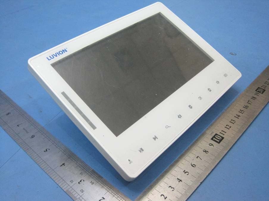
Click to zoom
Application Details
- Equipment Class
- DSS - Part 15 Spread Spectrum Transmitter
- Date of Grant
- Nov 28, 2011
- Application Purpose
- Original Equipment
- Date of Application
- Nov 28, 2011
- Equipment Note
- PREMIUM DIGITAL BABY MONITOR
- Frequency Range
- 2402.00000000 - 2480.00000000
- Company
- Egerium BV
- Country
- Netherlands
Documents & Files
Document Text
Text extracted from the exhibit documents filed with the FCC. Open a document above to read the original.
Block Diagram
BASEBAND 27MHZ 32.768KHZ CS8953 MCU 7' LCD Touch switch NOR FLASH DC-DC CONVERTER BATTERY MANGE AC-DC POWER ADAPTER MICROPHONE PA SPEAKER SDRAM RF IC 16MHZ SWITCH PA LPF
External Photos
Product View EUT – Appearence View
Internal Photos
EUT – Open View EUT - PCB View Screen – View RF Module – View Adapter – Open View Adapter – PCB View
Operational Description
Prestige Touch Camera Architecture: Prestige Touch Camera is a low cost and high performance digital Wireless camera which integrates M-JPEG codec , FHSS base band , RF transceiver ,CMOS sensor color processing unit , ADPCM codec, LCD display engine. The base- band implement a Bluetooth like frequency adaptive hopping technology to prevent being jammed by microwave oven and other 2.4GHz devices. It can co-existence with Bluetooth, WLAN and other 2.4GHz digital-modulated devices. Prestige Touch Camera hardware architecture is show in Block diagram z Auto ACK & retransmit On the air max. data rate 2Mpbs z Software selectable channel form 2400MHz to 2483.5MHz (37 Selectable channels) z Intelligent frequency hopping (change RF channel automatically) z Cmos sensor z Microphone z Audio amplifier z IR Leds nRF24L01 is a single chip radio transceiver for the world wide 2.4 -2.5 GHz ISM band. The transceiver consists of a fully integrated frequency synthesizer, a power amplifier, a crystal oscillator, a demodulator, modulator and Enhanced ShockBurst™ protocol engine. Output power, frequency channels, and protocol setup are easily programmable through a SPI interface. Current consumption is very low, only 9.0mA at an output power of -6dBm and 12.3mA in RX mode. Built-in Power Down and Standby modes makes power saving easily realizable. A simplified block diagram of the nRF24L01 is shown in figure 2 Figure 2 : nRF24L01 Block Diagram Packet Handling Methods nRF24L01 has the following Packet Handling Methods: ShockBurst™ (compatible with nRF2401, nRF24E1, nRF2402 and nRF24E2 with 1Mbps data rate, see page 24) Enhanced ShockBurst™ ShockBurst™ ShockBurst™ makes it possible to use the high data rate offered by nRF24L01 without the need of a costly, high-speed microcontroller (MCU) for data processing/clock recovery. By placing all high speed signal processing related to RF protocol on-chip, nRF24L01 offers the application microcontroller a simple SPI compatible interface, the data rate is decided by the interface-speed the micro controller itself sets up. By allowing the digital part of the application to run at low speed, while maximizing the data rate on the RF link, ShockBurst™ reduces the average current consumption in applications. In ShockBurst™ RX, IRQ notifies the MCU when a valid address and payload is received respectively. The MCU can then clock out the received payload from an nRF24L01 RX FIFO. In ShockBurst™ TX, nRF24L01 automatically generates preamble and CRC, see Table 12. IRQ notifies the MCU that the transmission is completed. All together, this means reduced memory demand in the MCU resulting in a low cost MCU, as well as reduced software development time. nRF24L01 has a three level deep RX FIFO (shared between 6 pipes) and a three level deep TX FIFO. The MCU can access the FIFOs at any time, in power down mode, in standby modes, and during RF packet transmission. This allows the slowest possible SPI interface compared to the average datarate, and may enable usage of an MCU without hardware SPI. Enhanced ShockBurst™ Enhanced ShockBurst™ is a packet handling method with functionality that makes bi-directional link protocol implementation easier and more efficient. In a typical bi-directional link, one will let the terminating part acknowledge received packets from the originating part in order to make it possible to detect data loss. Data loss can then be recovered by retransmission. The idea with Enhanced ShockBurst™ is to let nRF24L01 handle both acknowledgement of received packets and retransmissions of lost packets, without involvement from the microcontroller. Figure 3: nRF24L01 in a star network configuration An nRF24L01 configured as primary RX (PRX) will be able to receive data trough 6 different data pipes, see Figure 3. A data pipe will have a unique address but share the same frequency channel. This means that up to 6 different nRF24L01 configured as primary TX (PTX) can communicate with one nRF24L01 configured as PRX, and the nRF24L01 configured as PRX will be able to distinguish between them. Data pipe 0 has a unique 40 bit configurable address. Each of data pipe 1-5 has an 8 bit unique address and shares the 32 most significant address bits. All data pipes can perform full Enhanced ShockBurst™ functionality. nRF24L01 will use the data pipe address when acknowledging a received packet. This means that nRF24L01 will transmit ACK with the same address as it receives payload at. In the PTX device data pipe 0 is used to received the acknowledge, and therefore the receive address for data pipe 0 has to be equal to the transmit address to be able to receive the acknowledge. See Figure 5 for addressing example. Figure 4: Example on how the acknowledgement addressing is done An nRF24L01 configured as PTX with Enhanced ShockBurst™ enabled, will use the ShockBurst™ feature to send a packet whenever the microcontroller wants to. After the packet has been transmitted, nRF24L01 will switch on its receiver and expect an acknowledgement to arrive from the terminating part. If this acknowledgement fails to arrive, nRF24L01 will retransmit the same packet until it receives an acknowledgement or the number of retries exceeds the number of allowed retries given in the SETUP_RETR_ARC register. If the number of retries exceeds the number of allowed retries, this will show in the STATUS register bit MAX_RT and gives an interrupt. Whenever an acknowledgement is received by an nRF24L01 it will consider the last transmitted packet as delivered. It will then be cleared from the TX FIFO, and the TX_DS IRQ source will be set high. With Enhanced ShockBurst™ nRF24L01 offers the following benefits: Highly reduced current consumption due to short time on air and sharp timing when operating with acknowledgement traffic Lower system cost. Since the nRF24L01 handles all the high-speed link layer operations, like re-transmission of lost packet and generating acknowledgement to received packets, it is no need…
Text truncated - open the document above for the full version.
Schematics
1.3 1.3 7" DIGITAL MONITOR FOR LUVION RDI RDI940 RDI940 1 3 PCB NO: REV: MODEL NO: TITLE: COMPANY: REV: DATED: DATED: DATED: SIZE: SCALE: APPROVED: CHECKED: DRAWN: 1:1 A2 SHEET: OF Terry DNI DATA0 DATA1 DATA2 DATA3 SOUNDBAR power indication DNI DNI DNI 2011-10-17 DNI 27MHZ 32.768KHZ SPK1 8 OHM 1W Q1 MMBT3904 L2 BEAD B1 BEEP C53 22PF 0603 C54 22PF 0603 R67 33R 0603 R66 33R 0603 R68 220R 0603 R72 10K 0603 C56 1uF 0603 R76 470R 0603 R77 2.2K 0603 R78 NC 0603 R79 100K 0603 Q2 MMBT3904 R80 2.2K 0603 R93 0R 0603 D3 BAV70 R7 10K 0603 R11 10K 0603 MIC1 1 2 3 4 5 6 7 8 9 J3 R23 1.5K/NC 0603 R24 27R 0603 R25 27R 0603 R31 10K 0603 R32 100K 0603 R44 20K 0603 C27 104 0603 C29 0.33F D17 SS24 R10 10K 0603 1 OUT 2 GND 3 VCC IR1 R26 220R 0603 C18 DNI 0603 1 RTC1.8V 2 +5V 3 DGND 4 TV-OUT 5 HP_OUT 6 MIC_IN 7 MIC_GND 8 SPK_GND 9 SPK_OUT 10 NC 11 ADIN1 12 ADIN0 13 USB_MODE 14 RXD0 15 TXD0 16 DGND 17 NC 18 NC 19 NC 20 K6 21 K5 22 K4 23 K3 24 K2 25 K1 26 S_SCL 27 S_SDA 28 NC 29 DGND 30 SYS3.3V 31 LCD_BL_CNT 32 NC 33 NC 34 NC 35 NC 36 NC 37 NC 38 NC 39 NC 40 VUSB 41 USB_DP 42 USB_DN 43 DGND 44 PANEL_VSYNC 45 PANEL_HSYNC 46 PANEL_CLK 47 PANEL_D0 48 PANEL_D1 49 PANEL_D2 50 PANEL_D3 51 DGND 52 PANEL_D4 53 PANEL_D5 54 PANEL_D6 55 PANEL_D7 56 PANEL_FRAME 57 DGND 58 SPI_CLK 59 SPI_PCS 60 SPI_DATA U16 MR8990RX C34 104 0603 C45 104 0603 C68 220uF 3 IN 2 OUT 1 ADJ 4 U12 LM1117-3.3V 1 P0.5/PINT1.5/ADC2 2 P0.4/PINT1.4/ADB2 3 P0.3/PINT1.3/ADC1 4 P0.2/PINT1.2/ADB1 5 P0.1/PINT1.1/ADD1 6 P0.0/PINT1.0/ADA1 7 VDD25 8 VDD 9 RST 10 P2.7/CMPA/SWA0 11 P2.6/CMPB 12 P2.5/T2/CMPC 13 P2.4/T2EX/CMPD 14 P2.3/RXD1 15 P2.2/TXD1 16 P2.1/XOUT 17 P2.0/XIN 18 VSS 19 P1.7/T0/PINT0.1/SWB0 20 P1.6/T1/PINT0/SWB1 21 P1.3/SCL/SWB2 22 P1.2/SDA/SWC0 23 P1.5/RCOUT 24 P1.4/RXIN 25 P1.1/ADD4 26 P1.0/ADD3 27 P0.7/RXD0/ADD2 28 P0.6/TXD0/ADA2 U7 CS8953 SSOP-28 R97 1M 0603 C69 0.1uF 0603 R99 47K 0603 R103 120K 0603 R108 120K 0603 2 IN 3 OUT 1 GND U15 SOT_89 HT7533 C55 104 0603 R110 0R 0603 R105 47K 0603 TP2 TP3 TP4 TP5 TP1 R17 220R 0603 R15 4.7K 0603 4 1 2 3 L5 Comon Chock R18 10K 0603 C48 100uF ¡Ó5mm C51 10uF A C76 100uF ¡Ó5mm C28 10uF A R8 10K 0603 C49 10uF A C16 10uF A C15 100uF ¡Ó5mm SW3 SCAN SW6 TALK SW5 QUAD LED1 POWER LED2 LED3 LED4 LED6 SW2 video on/off SW4 Night-Light X1 49S 3.6864MHz 1 2 CON5-A 1 2 CON5-B 1 2 3 4 CON1-A 1 2 3 4 CON1-B 1 2 3 4 CON2-A 1 2 3 4 CON2-B 1 2 3 4 CON3-A 1 2 3 4 CON3-B 1 2 3 4 CON4-A 1 2 3 4 CON4-B 1 2 3 4 CON6 1 2 3 4 5 6 7 8 J5 R92 0R R94 DNI R95 47K SW7 ISPKEY R89 47K R55 0R 0603 R2 0R 0603 RXD0 TXD0 +3.3VA ALARM +5V +5V K1 K2 +3.3V +3.3VA +3.3VA IR VIDEO-OUT AUDIO-OUT RXD0 TXD0 K1 K2 SCL SDA +5V BACKLIGHT-EN VSYNC HSYNC CLK D0 D1 D2 D3 D4 D5 D6 D7 FRAME +3.3VA ALARM VDD LOWBATTERY VDD +3.3VA +BAT +3.3V PWM IR PWM AGND K1 LED3 AGND +3.3V LED2 LED4 P0.5 AGND LED6 AGND AGND NIGHT-LIGHT VIDEO_ON/OFF AGND SCAN K2 AGND +3.3V VIDEO-OUT AUDIO-OUT AV-DET AV-DET LED6 LED4 LED3 LED2 LED2 LED3 LED4 LED6 +3.3V ISPKEY +3.3VA +3.3V LOWBATTERY ISPKEY RTC_1V8 +1.8V 1.3 SHEET: OF A2 1:1 DRAWN: CHECKED: APPROVED: SCALE: SIZE: DATED: DATED: DATED: REV: COMPANY: TITLE: MODEL NO: REV: PCB NO: 3 2 RDI940 RDI940 1.3 RDI 7" DIGITAL MONITOR FOR LUVION R43 CHANGE FROM 4.7K TO 2.2K DIFFERENCE BETWEEN 20090623 AND 20091218 Terry 2011-10-17 26 AVSS 21 GND 1 GND 22 VR 23 VG 24 VB 19 CPH1 18 CPH2 17 CPH3 16 STHR 15 STHL 14 OEH 13 Q1H 12 LR 11 VCOM 10 VCOM 9 OEV 8 UD 7 CKV 6 STVL 5 STVR 4 VGH(+15V) 3 VGL(-10V) 25 AVDD 20 VCC 2 VCC J4 CON26 L13 0805 BEAD L12 0805 BEAD R35 10K 0603 R41 DNI 0603 R42 33R 0603 L14 0805 BEAD C65 104 0603 L15 100uH R43 2.2K 0603 C77 102 0603 D12 RB411D R47 9.1K 0603 R48 1.3K 0603 K A ZD1 UDZ15B R50 DNI 0603 C83 470nF 0603 1 2 3 D15 BAT54S ZD2 UDZ10B C89 1uF 0603 1 1OUT 2 1IN- 3 1IN+ 4 GND 5 2IN+ 6 2IN- 7 2OUT 8 VCC U10 RC4558D R52 10K 0603 R57 10K 0603 R59 10K 0603 R60 22K 0603 C90 10uF 1206 VR1 50K R61 1K 0603 R62 22K 0603 VR2 50K R74 DNI 0603 L16 100uH C93 104 0603 L17 0805 BEAD C97 104 0603 L18 0805 BEAD C13 104 0603 C14 104 0603 1 HS 2 VS 3 SCL 4 SDA 5 RSTN 6 VDD3 7 VSS3 8 RSEL 9 VDD2 10 VSS2 11 12 13 14 15 16 17 VSSA3 18 19 20 21 22 23 24 25 26 27 VCCA3 28 29 30 31 32 VSSA3 96 VSSA-DAC3 95 VCCA-DAC3 94 DAC-B 93 DAC-G 92 VSSA-DAC2 91 VCCA-DAC2 90 DAC-R 89 DAC-COMP 88 DAC-REXT 87 VSSA-DAC1 86 VCCA-DAC1 85 DCFBK3 84 DCFBK2 83 DCFBK1 82 DCPCM3 81 DCPCM2 80 DCPCM1 79 PWM3 78 PWM2 77 PWM1 76 VDD33 75 VSS33 74 VSSA25-PLL 73 VCCA25-PLL 72 71 VDD2 70 VSS2 69 GP1 68 GP2 67 GP3 66 65 97 98 R 99 G 100 B 101 102 CPH1 103 CPH2 104 CPH3 105 106 VSS2 107 VDD2 108 PRG0 109 PRG1 110 PRG2 111 PRG3 112 PRG4 113 PRG5 114 PRG6 115 PRG7 116 VSS3 117 VDD3 118 ADC0 119 ADC1 120 121 122 123 124 125 126 127 128 64 STHL 63 STHR 62 CLKV 61 STVU 60 STVD 59 LP 58 POL 57 HME 56 VSS3 55 VDD3 54 D7 53 D6 52 D5 51 D4 50 D3 49 D2 48 D1 47 D0 46 CLK 45 C-HS 44 C-CS 43 C-FID 42 VDD2 41 VSS2 40 TESTS 39 TESTA 38 VSS2A-O 37 VCC2A-O 36 VSS2A-I 35 34 33 U11 CT674 R75 10K 0603 R81 10K 0603 L19 0805/0R C2 104 0603 L20 0805 0R C60 104 0603 C64 104 0603 R82 DNI 0603 R83 0R 0603 L21 DNI C32 22PF 0603 C47 22PF 0603 R84 1M 0603 L22 BEAD R85 1.5K 0603 C46 104 0603 R87 75R 0603 C111 47uF ¡Ó8mm C11 104 0603 C57 104 0603 C43 104 0603 C95 104 0603 Q6 2SC4672 C10 104 0603 C20 104 0603 1 2 J2 LED BACKLIGHT 2 GND 4 EN 6 VDD 1 SW 3 FB 5 OV U5 MP3202D L4 10uH D10 SS24 C24 105 1206 R13 0R 0603 R14 4.7K 0603 R16 1R 0805 C3 104 0603 R9 0R 0603 C50 100NF 0603 C67 10uF A C70 10uF A C72 10uF A C12 10uF A R19 10K 0603 X2 24.576MHz R21 75R 0603 R22 75R 0603 C73 10uF 1206 R36 DNI 0603 R33 DNI 0603 R34 10K 0603 R37 10K 0603 C80 10uF 0805 C74 10uF 0805 C75 104 0603 C79 470nF 0603 C85 470nF 0603 C86 470nF 0603 C82 1uF 0603 C84 1uF 0603 C81 104 0603 C88 104 0603 C91 220uF ¡Ó8mm C87 100uF ¡Ó8mm C78 56pF 0603 R49 220R 0603 R51 220R 0603 R54 100K 0603 R58 100K 0603 C58 10uF A C61 10uF A C66 10uF A C59 104 0603 C63 104 0603 C71 104 0603 1 2 3 D16 BAT54S 1 2 3 D14 BAT54S 1 2 3 D13 BAT54S TP6 TP7 STVD STVU CLKV VCOM OEV +5VD UDC LRC OEH STHL STHR VR VG VB CPH1 +5V PWM0 +3.3V FBK0 POL +5VD +5VD VCO…
Text truncated - open the document above for the full version.
Test Report
Page: 1 of 52 Egerium BV FCC ID: Z5MLUVPTMON FCC TEST REPORT The results shown in this test report refer only to the sample(s) tested , This Test report cannot be reproduced, except in full, without prior written permission of the Company. WALTEK SERVICES Reference No.: WT11105895-S-E-F FCC ID : Z5MLUVPLAT2MON Applicant : Egerium BV Address : Kleveringweg 25, 2616LZ Delft Netherlands Equipment Under Test (EUT) : Product Name : Premium Digital Baby Monitor Model No. : LUVION PRESTIGE TOUCH Standards : FCC CFR47 Part 15 Section 15.247:2009 Date of Test : November 1~21, 2011 Date of Issue : November 21, 2011 Test Engineer : Zero Zhou /Engineer Reviewed By : Philo Zhong/Manager Test Result : PASS Prepared By: Waltek Services (Shenzhen) Co., Ltd. 1/F, Fukangtai Building, West Baima Rd., Songgang Street, Baoan District, Shenzhen 518105, China Tel :+86-755-27553488 Fax:+86-755-27553868 The sample detailed above has been tested to the requirements of Council Directives ANSI C63.4:2009. The test results have been reviewed against the Directives above and found to meet their essential requirements. Page:2 of 52 Egerium BV FCC ID: Z5MLUVPTMON The results shown in this test report refer only to the sample(s) tested , This Test report cannot be reproduced, except in full, without prior written permission of the Company. WALTEK SERVICES Reference No.: WT11105895-S-E-F 2 Test Summary Test Items Test Requirement Result Radiated Spurious Emissions (9kHz to 25GHz) 15.205(a) 15.209 15.247(d) PASS Conduct Emission 15.207 PASS 20dB Bandwidth 15.247(a)(1) PASS Maximum Peak Output Power 15.247(b)(1) PASS Frequency Separation 15.247(a)(1) PASS Number of Hopping Frequency 15.247(a)(1)(iii) PASS Dwell time 15.247(a)(1)(iii) PASS Maximum Permissible Exposure (Exposure of Humans to RF Fields) 1.1307(b)(1) PASS Page:3 of 52 Egerium BV FCC ID: Z5MLUVPTMON The results shown in this test report refer only to the sample(s) tested , This Test report cannot be reproduced, except in full, without prior written permission of the Company. WALTEK SERVICES Reference No.: WT11105895-S-E-F 3 Contents 1 COVER PAGE........................................................................................................................................................ 1 2 TEST SUMMARY .................................................................................................................................................. 2 3 CONTENTS............................................................................................................................................................. 3 4 GENERAL INFORMATION ................................................................................................................................ 4 4.1 CLIENT INFORMATION........................................................................................................................................... 4 4.2 GENERAL DESCRIPTION OF E.U.T. ........................................................................................................................ 4 4.3 DETAILS OF E.U.T................................................................................................................................................. 4 4.4 DESCRIPTION OF SUPPORT UNITS.......................................................................................................................... 4 4.5 STANDARDS APPLICABLE FOR TESTING................................................................................................................ 4 4.6 TEST FACILITY...................................................................................................................................................... 5 4.7 TEST LOCATION.................................................................................................................................................... 5 5 EQUIPMENT USED DURING TEST .................................................................................................................. 6 6 CONDUCTED EMISSION .................................................................................................................................... 7 7 RADIATED SPURIOUS EMISSIONS ............................................................................................................... 12 8 RADIATED EMISSIONS WHICH FALL IN THE RESTRICTED BANDS................................................. 23 9 20 DB BANDWIDTH MEASUREMENT........................................................................................................... 28 10 MAXIMUM PEAK OUTPUT POWER ............................................................................................................. 30 11 HOPPING CHANNEL SEPARATION .............................................................................................................. 31 12 NUMBER OF HOPPING FREQUENCY .......................................................................................................... 34 13 DWELL TIME ...................................................................................................................................................... 35 14 ANTENNA REQUIREMENT ............................................................................................................................. 38 15 RF EXPOSURE .................................................................................................................................................... 38 16 PHOTOGRAPHS - CONSTRUCTIONAL DETAILS...................................................................................... 40 16.1 PRODUCT VIEW.............................................................................................................................................. 40 16.2 EUT – APPEARENCE VIEW............................................................................................................................. 41 16.3 EUT – OPEN VIEW.....................................…
Text truncated - open the document above for the full version.
Test Setup Photos
Photograph – Conducted Emission Test Setup Photograph – Radiation Spurious Emission Test Setup Below 1GHz Above 1GHz
Contact Information
Applicant
Michiel Pannekoek(Manager)
Test Firm
Waltek Services(Shenzhen) Co., Ltd.Philo zhong
Technical Specifications
| # | Rule Parts | Frequency Range | Power Output |
|---|---|---|---|
| 1 | 15C | 2.40 GHz - 2.48 GHz | 13.00 mW |
Other Applications from Egerium BV
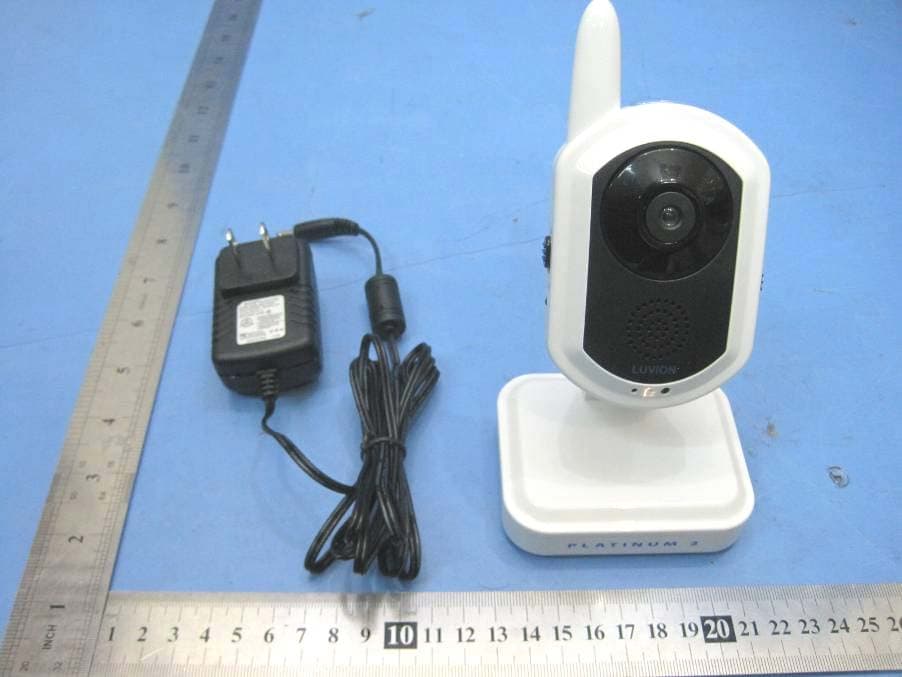
Z5MLUVPLAT2CAM
Nov 28, 2011PREMIUM DIGITAL CAMERA
Equipment Class
DSS - Part 15 Spread Spectrum Transmitter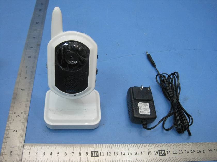
Z5M-LUVGECAM
Nov 07, 2011DIGITAL WIRELESS CAMERA AND MONITOR SYSTEM
Equipment Class
DSS - Part 15 Spread Spectrum Transmitter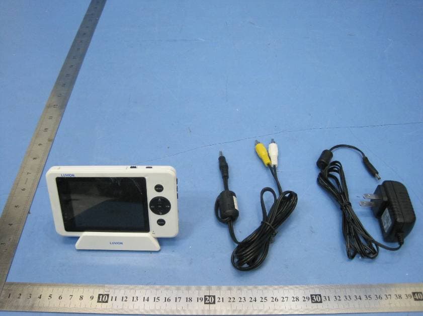
Z5M-LUVGEMON
Nov 07, 2011DIGITAL WIRELESS CAMERA AND MONITOR SYSTEM
Equipment Class
DSS - Part 15 Spread Spectrum Transmitter