ZBA8543709200CCell Phone Signal Booster
Global Horwey Corp Ltd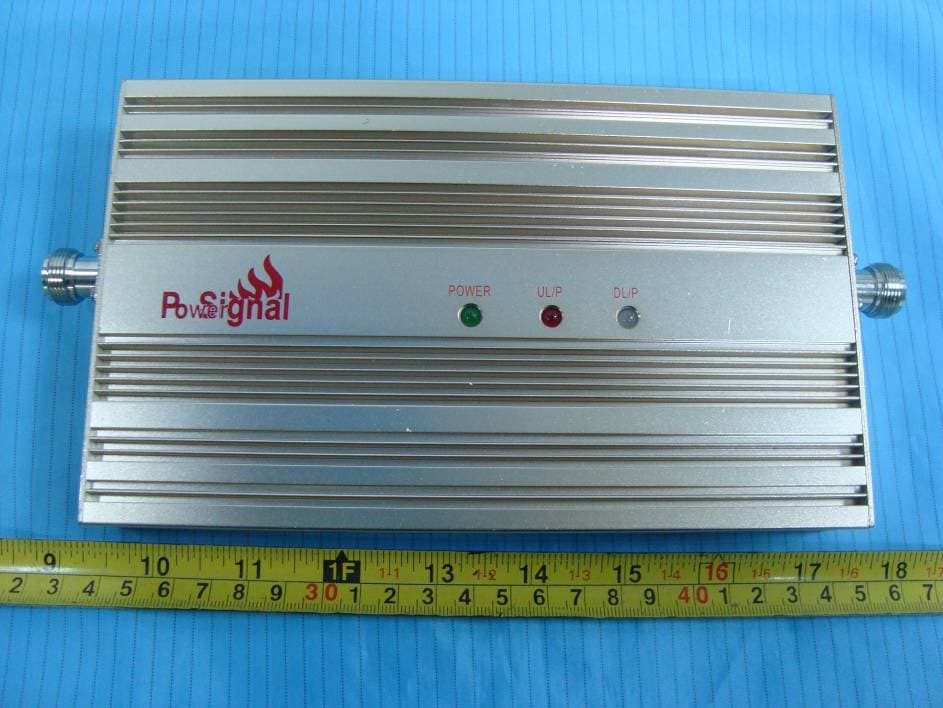
Click to zoom
Application Details
- Equipment Class
- AMP - Amplifier
- Date of Grant
- Apr 20, 2011
- Application Purpose
- Original Equipment
- Date of Application
- Apr 20, 2011
- Equipment Note
- Cell Phone Signal Booster
- Frequency Range
- 869.00000000 - 894.00000000
- Company
- Global Horwey Corp Ltd
- Country
- United States
Documents & Files
Document Text
Text extracted from the exhibit documents filed with the FCC. Open a document above to read the original.
Users Manual
- 1 - Preface series signal booster. The detailed User Manual is attached to th is machine so that you can get familiar to operate it as soon as possible, from wh ich you will get the in formation of product introduction, operation instructions, system settings and safety precautions, etc. This product is suitable for operation of mobile phones in a weak signal area! We appreciate you selecting the GSM800MHz - 2 - Contents 1. Purposes..................................................................................................................3 2. Technical features....................................................................................................4 3. Technical specifications...........................................................................................5 4. System configuration...............................................................................................6 5. Operation instructions..............................................................................................7 5.1. Descriptions of the overall dimension of the equipment.................................7 5.2. Instructions on installation..............................................................................8 5.3. Debugging and commissioning......................................................................9 5.4. System maintenance.....................................................................................10 6. Descriptions on maintenance.................................................................................10 6.1. Faults and failures.........................................................................................10 6.2. Troubleshooting .........................................................................................10 6.3 Optimization & troubleshooting ................................................................................11 - 3 - User Manual of Signal Booster 1. Purpose As the domestic mobile communication industry develops rapidly, the amount of mobile communications users increases so steadily that the cell planning gets smaller and smaller while the base station positions get lower and lower. On the other hand, as city construction develops, more and more high-rise buildings are set up constantly, based on the shadow effect of the radio propagation, the mobile communications may get a signal blind spot behind or between the buildings. Moreover, in order to avoid interference from adjacent districts, the main lobe of the antenna radiation orientation of the cell mobile communication base station in construction has a bigger down-tilt obliquity, thus the signals usually can not be received effectively in the high and medium parts of the high rise buildings. Furthermore, due to the shield effect to electro-magnetic waves caused by buildings, the mobile communication signals cannot be received in tunnels, subways, underground stores, entertainment complex, parking fields, hotels, office buildings and other large-size and closed buildings. Signal amplifier is an effective device that makes up the insufficient base station coverage in the mobile network, enlarges the coverage area of the base station and fills in the blind spots, which adopts double-ended duplex design and external power supply with advantages of convenient mounting and high reliability. The bandwidth of the signal amplifier may cover 800MHz with compatibility between digital system and analogue system. - 4 - 2. Technical features ● High system gains ● Full duplex and double-end design, external power supply, and convenient installation ● ALC technology with auto-steady function adopted. ● Provide power indication and uplink and downlink indications. ● With the amplified linear power, the intermodulation and spuriousness are suppressed effectively. ● The reliability conforms to GB6993-86 standards. ● The electromagnetic compatibility conforms to ETS300 609-4 standards. - 5 - 3. Technical specifications Frequency Range Uplink: 824 - 849MHz, Downlink: 869 -894MHz Model PS-170 Output Power 20±1dBm Gain UL: 65±2dB, DL: 70±2dB Ripple Pass Band ≤6dB Noise Figure ≤6dB Group Delay ≤5μs ALC Range ≥ 20dB VSWR ≤1.8 Spurious Emission 9KHz--1GHz: ≤-36dBm/100KHz 1GHz--12.75GHz: ≤-30dBm/1MHz Inter-modulation ≤-40dBc Other Specification I/O Impedance 50Ω RF Connector N-Female Operation Temp. -10 - +50 °C Humidity ≤95% Dimensions Approx. 200×120×30mm Weight Approx. 1.5kg Power Supply AC:100V-240V, 50-60Hz DC:5V- 3A - 6 - 4. System structure A simple signal amplifier system is composed of a host signal amplifier,reverse antenna and in-door covering system. Reverse antenna aims at the reverse base station that requires for expanding the coverage, the BTS Port of the host signal amplifier is connected with reverse antenna and User’s Port is connected with in-door covering system. As shown in the following diagram, firstly, the indoor signals introduced by the signal amplifier are divided into two-way signals by splitters, then each signal is distributed two antennas through a coupler with the power distribution ratio equal to circuit exhaust ratio so as to ensure both of the antennas to obtain equal power (splitter and coupler may can be configured flexibility). It shall be attached importance that at least 15dB of the isolation shall be bigger than the plus between reverse antenna and covering system for meeting the requirements of C/I≥15dB of the 800MHz system. System structure diagram - 7 - 5. Operation instructions 5.1. Descriptions of the overall dimension of the equipment The whole-set shape is shown as follows: Indication Specification: A. OUTDOOR: to be connect outdoor antenna. B. INDDOOR: to be connect indoor antenna. C. POWER: when normal working, power status is green. D.UL / P: when normal working or calling, up link status is red. E. DL / P: when normal working, down link status is red. F. DC+5V: power supply - 8 - 5.2 Instructions on installation 1. Firstly, select …
Text truncated - open the document above for the full version.
External Photos
EXHIBIT B - EUT EXTERNAL PHOTOGRAPHS EUT – Top View EUT – Bottom View EUT – Side View EUT – Port View
ID Label/Location Info
EXHIBIT A - FCC ID LABELING AND LOCATION FCC ID Label FCC ID Label Location Label here The label shown shall be permanently affixed at a conspicuous location on the device and be readily visible to the user at the time purchase (Labeling requirements per 2.925)
Internal Photos
EXHIBIT C - EUT INTERNAL PHOTOGRAPHS EUT – Cover off View EUT – Main Board Top view EUT – Main Board Bottom view
Parts List/Tune Up Info
1 BOM Product name 3AN009 Products number Document name Edition number Put into date: quantity No. Name: Model: Packa ge Location Numb er To t a l 1 Capacitors 3P 0805 C79 C98 C158 3 2 Capacitors 7P 0805 C114 C123 2 3 Capacitors 10P 0603 C1 1 4 Capacitors 10P 0805 C47 1 5 capacitors 15P 0805 C110 C117 2 6 capacitors 47P 0805 C6 C11 C12 C19 C21 C27 C28 C53 C54 C59 C66 C67 C72 C149 C159 C165 16 7 capacitors 101P 0603 C3 C8 C15 C31C38 C46 C50 C56 C61 C70 C75 C80 C83 C85 C87C92 C95 C101 C103 C104 C108 C112 C115 C24 34 8 capacitors 101P 0805 C78 C118 C124 3 9 capacitors 102P 0603 C13 C14 C40 C60 C63 C102 C146 7 10 capacitors 103P 0603 C2 C7 C22 C29 C48 C55 C68 C74 C150 C166 10 11 capacitors 104P 0603 C4 C9 C16 C18 C23 C30 C39 C44 C45 C51 C57 C62 C65 C69 C81 C84 C88 C90 C93 C94 C113 C116 C122 C126 C147 C152 C155 C168 C76 29 12 capacitors 105P 0805 C17 C64 C111 C120 C127 5 13 capacitors 106P 1206 C5 C10 C25 C32 C52 C58 C71 C77 C82 C96 C153C157 C169 13 14 capacitors 224P 0603 C43 C86 2 15 Electrolytic Capacitor 470u/16v RB6.6 C91 1 Resistors 0R 0805 R7 ,R97, R15, 3 16 Resistors 0R 1206 R1 R10 R56 ,R99 4 17 Resistors 10R 0805 R6 R51 2 18 Resistors 10R 1206 R13 ,R59 2 19 Resistors 13R 0805 R52 ,R65, R100 3 2 20 Resistors 30R 1210 R50 R92 2 21 Resistors 51R 0603 R81 R82 R95 R96 4 22 Resistors 51R 0805 R37 R67 2 23 Resistors 101 0603 R25 R34 R35 R76 R77 5 24 Resistors 471 0603 R23 R73 2 25 Resistors 511 0603 R66 R94 2 26 Resistors 681 0603 R8 R14 R28 R53 R54 R58 6 27 Resistors 102 0603 R18,R24,R29,R30,R68,R91, R101,R102,R103 9 28 Resistors 152 0603 R9 R11 R55 R57 4 29 Resistors 202 0603 R27 R74 2 30 Adjustable Resistance 202 VR5A RJ1 RJ2 2 31 Resistors 302 0603 R26 1 32 Resistors 391 0603 R87 R93 2 33 Resistors 512 0603 R12 R19 R20 R31R32 R69 R70 7 34 Resistors 682 0603 R71 R75 2 35 Resistors 123 0603 R21 1 36 Resistors 333 0603 R33 1 37 Inductors 1NH 0603 L22 L26 2 38 Chip Inductors 5N6 0603 L23 L24 2 39 Inductors 5N6 0805 L9 L21 2 40 Inductors 39NH 0805 L10 L27 2 41 Inductors 68NH 0805 L2 L3 L4 L5 L6 L7 L11 L12 L13 L14 L15 L17 L18 L25 L28 L29 L31 17 42 Inductors 180NH 1206 L1 L19 L20 3 43 Voltage Regulator 11117-3.3 11117-3. 3 U2 1 IC A Q2, Q3,Q11, 3 44 IC A62 SOT-89 Q7, Q9, Q13 3 45 IC ATF34143 SOT-343 Q1 Q6 2 46 IC HSM2820 SOT-23A HS1 HS2 2 3 47 IC HSMP381 4 SOT-23A HP1 HP2 HP3 HP4 4 48 IC LM33202 SO-8 IC3 1 49 IC LM2902 SO-14 IC2 1 50 IC RF2192 RF2174 Q5 Q10 2 51 IC LED2 SP3 LED2 1 52 IC LEDP LED LED3 1 53 IC MBRS340 IN5822 D1 1 54 Diplexer DFY2R90 2 DFD902/ 947 DB1 1 55 Diplexer HP947/90 2 HP947/9 02 DB2 1 56 Isolator 897 ISO7 ISO4 1 57 Isolator 950 ISO7 ISO1 1 58 SAW GB(4684) RFSAW X1 X2 X3 X4 X5 5 59 SAW .M RFSAW X6 X7 X8 3 60 SAW 9037 RFSAW X9,X10 2 61 Power Connector CON2 5V/3A1 J1 1 Diplexer KF7R836 E881 DB1 1 Diplexer HP836/88 1 DB2 1 Isolator 836 ISO7 ISO4 1 Isolator 881 ISO7 ISO22 1 SAW AC RFSAW X1 X2 X3 X4 X5 5 CD MA SAW A7 RFSAW X6 X7 X8 X9 X10 5 62 Steel 3AN009 1 63 PCB 3AN009 1
RF Exposure Info
Global Horwey Corp. Ltd. FCC ID: ZBA8543709200C Report No.: RDG11022101-22H Page 8 of 56 FCC Part 22H Test Report FCC §1.1307 & §2.1091- MAXIMUM PERMISSIBLE EXPOSURE (MPE) Applicable Standard According to FCC §1.1307 (b)(1) and §2.1091 systems operating under the provisions of this section shall be operated in a manner that ensures the public is not exposed to RF energy level in excess of the communication guidelines. Limits for General Population/Uncontrolled Exposure Limits for General Population/Uncontrolled Exposure Frequency Range (MHz) Electric Field Strength (V/m) Magnetic Field Strength (A/m) Power Density (mw/cm 2 ) Averaging Time (Minutes) 0.3-1.34 614 1.63 *(100) 30 1.34-30 824/f 2.19/f *(180/f 2 ) 30 30-300 27.5 0.073 0.2 30 300-1500 / / f/1500 30 1500-100,000 / / 1.0 30 f = frequency in MHz * = Plane-wave equivalent power density MPE Predication Predication of MPE limit at a given distance S = PG/4πR² Where: S = power density (in appropriate units, e.g. mW/cm 2 ) P = power input to the antenna (in appropriate units, e.g., mW). G = power gain of the antenna in the direction of interest relative to an isotropic radiator, the power gain factor, is normally numeric gain. R = distance to the center of radiation of the antenna (appropriate units, e.g., cm) Antenna Gain Conducted Power Mode Frequency (MHz) (dBi) (numeric)(dBm)(mW) Evaluation Distance (cm) Power Density (mW/cm 2 ) MPE Limit (mW/cm 2 ) Cellular Band (GSM) Uplink 824.20 9 7.9 19.12 83.18 20 0.131 0.5495 Downlink 881.60 9 7.9 19.60 91.20 20 0.143 0.5877 Cellular Band (CDMA) Uplink 824.70 9 7.9 18.77 75.33 20 0.118 0.5498 Downlink 881.52 9 7.9 19.45 88.10 20 0.139 0.5877 Result: The deice meets FCC MPE limit at 20 cm distance.
Test Report
Note: This test report is prepared for the customer shown above and for the device described herein. It may not be duplicated or used in part without prior written consent from Bay Area Compliance Laboratories Corp. This report must not be used by the customer to claim product certification, approval, or endorsement by NVLAP*, NIST, or any agency of the Federal Government. * This report contains data that are not covered by the NVLAP accreditation and are marked with an asterisk “★” (Rev.2) FCC PART 22H MEASUREMENT AND TEST REPORT For Global Horwey Corp. Ltd. 2847 Eaglecrest PL .Walnut, CA 91789, USA FCC ID: ZBA8543709200C Report Type: Original Report Product Type: Cell Phone Signal Booster Test Engineer: Alvin Huang Report Number: RDG11022101-22H Report Date: 2011-04-20 Reviewed By: Merry Zhao EMC Engineer Prepared By: Bay Area Compliance Laboratories Corp. (Shenzhen) 6/F, the 3rd Phase of WanLi Industrial Building, ShiHua Road, FuTian Free Trade Zone Shenzhen, Guangdong, China Tel: +86-755-33320018 Fax: +86-755-33320008 Global Horwey Corp. Ltd. FCC ID: ZBA8543709200C Report No.: RDG11022101-22H Page 2 of 56 FCC Part 22H Test Report TABLE OF CONTENTS GENERAL INFORMATION.......................................................................................................................................3 PRODUCT DESCRIPTION FOR EQUIPMENT UNDER TEST (EUT) .....................................................................................3 OBJECTIVE...................................................................................................................................................................3 RELATED SUBMITTAL(S)/GRANT(S).............................................................................................................................3 TEST METHODOLOGY..................................................................................................................................................3 TEST FACILITY.............................................................................................................................................................4 SYSTEM TEST CONFIGURATION ..........................................................................................................................5 JUSTIFICATION.............................................................................................................................................................5 EQUIPMENT MODIFICATIONS.......................................................................................................................................5 LOCAL SUPPORT EQUIPMENT LIST AND DETAILS........................................................................................................5 EXTERNAL I/O CABLE..................................................................................................................................................5 CONFIGURATION OF TEST SETUP.................................................................................................................................5 BLOCK DIAGRAM OF TEST SETUP................................................................................................................................6 SUMMARY OF TEST RESULTS ...............................................................................................................................7 FCC §1.1307 & §2.1091- MAXIMUM PERMISSIBLE EXPOSURE (MPE).............................................................8 APPLICABLE STANDARD..............................................................................................................................................8 MPE PREDICATION......................................................................................................................................................8 FCC §2.1047 - MODULATION CHARACTERISTIC ..............................................................................................9 FCC § 2.1046, § 22.913 (A) - RF OUTPUT POWER ...............................................................................................10 APPLICABLE STANDARD............................................................................................................................................10 TEST PROCEDURE......................................................................................................................................................10 TEST EQUIPMENT LIST AND DETAILS.........................................................................................................................10 TEST DATA................................................................................................................................................................10 FCC §2.1049, §22.917 & §22.905 - OCCUPIED BANDWIDTH .............................................................................12 APPLICABLE STANDARDS...........................................................................................................................................12 TEST PROCEDURE......................................................................................................................................................12 TEST EQUIPMENT LIST AND DETAILS.........................................................................................................................12 TEST DATA................................................................................................................................................................12 FCC §2.1051, §22.917(A) - SPURIOUS EMISSIONS AT ANTENNA TERMINALS ..........................................27 APPLICABLE STANDARDS...........................................................................................................................................27 TEST PROCEDURE....................................................................................................................................................…
Text truncated - open the document above for the full version.
Test Setup Photos
EXHIBIT D - TEST SETUP PHOTOGRAPHS Below 1 GHz: Spurious Radiated Emissions – Front View Below 1 GHz: Spurious Radiated Emissions – Rear View Above 1 GHz: Spurious Radiated Emissions – Front View Above 1 GHz: Spurious Radiated Emissions – Rear View
Contact Information
Applicant
Henry Hou
Test Firm
Bay Area Compliance Laboratory Corp. (Shenzhen)John Chan
Technical Specifications
| # | Rule Parts | Frequency Range | Power Output | Emission | Tolerance |
|---|---|---|---|---|---|
| 4 | 22H | 869 MHz - 894 MHz | 100.00 mW | F9W | Amp |