ZBF88888HSUPA WIRELESS MODEM
Shenzhen Mobidata Communication Technology Co., Ltd.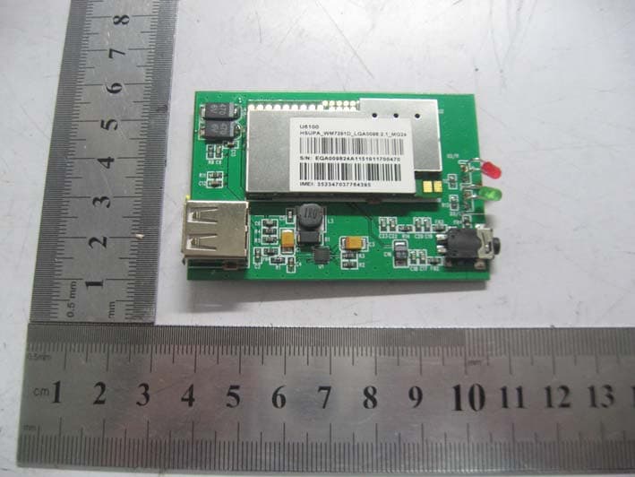
Click to zoom
Application Details
- Equipment Class
- PCB - PCS Licensed Transmitter
- Date of Grant
- Mar 13, 2011
- Application Purpose
- Original Equipment
- Date of Application
- Mar 13, 2011
- Equipment Note
- HSUPA WIRELESS MODEM
- Frequency Range
- 1852.40000000 - 1907.40000000
- Country
- China
Documents & Files
Document Text
Text extracted from the exhibit documents filed with the FCC. Open a document above to read the original.
Users Manual
HSPA/UMTS/WCDMA/EDGE/GPRS/GSM USB MODEM 220HU (Quick Start) 1 1 About 220HU USB MODEM The 220HU USB MODEM is designed to enable PC user access to Internet via GPRS/EDGE/WCDMA/UMTS/HSPA network. This mode uses a standard USB interface for a fast simple connection to your PC. As to 220HU USB MODEM, which is designed based on HSPA technology with multi-chipsets, support 3G technology, as well as 2G technology. Functions: y Access to Internet by wireless connection with high speed y Send and receive messages y Contact Manager y Volume statistics y Hardware support voice calling, y Auto search-register wireless network, y Zero CD, plug and play on Windows, y Micro SD, T-Flash supported, Technology Parameter y Multi-chipsets scheme, y HSUPA/HSDPA/UMTS 850/1900, y EDGE/GRPS/GSM 850/1900MHz, y HSPA:7.2Mbps Downlink rate, 2Mbps Uplink rate, Update to 5.76Mbps, y UMTS/WCDMA: 384Kbps Downlink and Uplink rate, y EDGE: 384Kbps Downlink rate,177Kbps Uplink rate, y GPRS/GSM:115.2Kbps downlink rate, 57.6Kbps uplink rate, y Windows 2000/xp(Basic home, Professional)/vista(Basic home, Business), Mac OSX y HSUPA/HSDPA/UMTS/WCDMA/EDGE/GPRS/GSM network compatible, y English version y GSM SIM, 3G, 3.5G USIM y -10°C~+50°C working temperature y Dimension/Weight 83*29*12mm/35g PC Configures(Suggested) y Win2000 sp4, XP sp2,sp3, Vista, Mac y At least 800×600 pixs, y At least 1GHz processor, 256M memory, 100M Hard disk. y At least one free USB port HSPA/UMTS/WCDMA/EDGE/GPRS/GSM USB MODEM 220HU (Quick Start) 2 Insert (U)SIM or T-Flash y Before connect modem to PC, please insert (U)SIM like the picture, y If you want to use T-Flash, please plug out the modem then insert T-Flash like the picture, 2 Installations 2.1 Getting Started Remove the USB cover and insert (U) SIM into the slot according to direction shown in figure. Ensure that U (SIM) has been inserted completely. 2.2 Connect 220HU USB MODEM to PC a) Insert the USB MODEM into a USB port on the computer according to direction shown in figure as below, or connect to the PC with a USB cable; b) Ensure that has been inserted completely. If indicator light twinkled in red. c) Installation program should run automatically after the MODEM insertion into the computer correctly; in case of failure in the automatic run, please open MODEM folder via Icon of My Computer in Windows OS, and double click it to begin installing. d) Program should run automatically if installation is completed. e) If both automatic running and MODEM folder unavailable, it may be blocked by the antivirus software on the computer, such as Kaspersky. Please exit the modem software, and close or exit the antivirus software temporarily, then insert and install again. Please notice. 2.3 Install on Windows XP Before installation please confirm the system configuration. The required is Pentium 1GHz or advanced CPU, 512MB or advanced memory and 100MB disk at least. (1). Choose the right item in the option list of languages, and click “OK” to install the driver firstly. (2). Select the directory path to install the driver. It may need seconds to install the HSPA/UMTS/WCDMA/EDGE/GPRS/GSM USB MODEM 220HU (Quick Start) 3 driver, please wait a moment here. (3). After driver installed, please click “Finish” to run the software. (4). If saying “no device” or” fail to connect” in the software, it may be the result of failed driver installation. Please reinsert the modem, if asking for driver please let it search automatically. Remaks: On Windows 98/2000, it is the same way to install software, but you need to reboot the computer after software installation. 2.4 Install on Windows Vista (1). Because of the safety function of Vista, the UAC will remind you the EXE files when install software. If that please select “Allow” like the following picture. (2). Besides the up different steps, others are the same with steps on Windows XP. 3 Operation of Software 3.1 Entrance to main interface (1). Application runs automatically and main interface pops up when plug the device in for 2nd time. Also, you can find and run the application in the <start> menu. (2). If you enabled the PIN code, please input the right PIN code in input field, and click <OK>. You have only 3 attempts to input the PIN code, otherwise SIM/USIM card will be locked after 3 times’ failure. An input PUK code window will appear which tells you should input the right PUK code, and then click <OK>, the default new PIN code is 0000. If you fail to input the right PUK code after 10 times, please contact your operator. 3.2 Main interface instruction Function icon : Connect to Internet : Open SMS contacts management interface : Open contacts management interface : Set parameters of device and software State information HSPA/UMTS/WCDMA/EDGE/GPRS/GSM USB MODEM 220HU (Quick Start) 4 : Indicate signal strength of current network Network type: Display GSM/UMTS when network is available but disconnected to Internet, Display GPRS/UMITS/HSPDA when connected to Internet Operator: Display the corresponding operator’s name according to SIM/USIM card : Indicate unread SMS in main interface Tray Icon Click icon,the application becomes a tray icon in system tray. Main interface can be reopened by double click it. 3.3 Establish connection Connect 1. Clicking on main interface to connect Internet, of which operation change to; 2. Internet connection is established successfully if connection information window ejects. Please check APN setting if connection failed. (Refer to the section of custom connection in Help.) Disconnect Click on main interface to disconnect Internet. 3.4 SMS service Click icon in the main interface to open SMS/contacts management interface, and choose <messages> to enter SMS service interface. Update 1. Click <send/receive>button in shortcut menu bar; 2. Messages saved in SIM card will be read and displayed in the right column. The application will update the new received message, which a window at the right corner of the PC will pop up when you have…
Text truncated - open the document above for the full version.
Block Diagram
MBD-220 Block Diagram Main Board U6100 MODULE USB Interface USB power 3G SIM card Audio Interface 3G Antenna Green_3G Led Red_Power Ant. GSM/GPRS/EDGE850/1900 & WCDMA/HSUPA/HSDPA Band II/V RF Connector/ Main Antenna RF TRANSCEIVER RTR6280 Multimodel Antenna Switch GSM850/Receiver Match GSM1800/1900 Transmitting GSM900/850 Transmitting GSM900/Receiver Match GSM1800/Receiver Match GSM1900 /Receiver Match MCP Baseband Processor MSM6290 60-pin,0.5mm Pitch Socket (USB,USIM,Power and so on) TCXO 19.2 Mhz XTAL 32.768 Khz Power Manager PM6653 UMTS BC1 2100MHz PA UMTS BC2 1900MHz PA UMTS BC5 850MHz PA BC1 2100MHz Duplexer BC2 1900MHz Duplexer BC5 850MHz Duplexer GSM PA Power Buffer MSM_TCXO RTR6285_TCXO Power Power USB_TCXO SLEEP_CLK
ID Label/Location Info
Shenzhen Mobidata Communication Technology Co., Ltd Model: MBD-220HU REPORT NO.: STR11028094I-1 FCC PART 22&24 EXHIBIT 1- PRODUCT LABELING Proposed FCC ID Label Format FCC ID: ZBF88888 Specifications : Text is Black in color and justified. Labels are printed in indelible ink on permanent adhesive silk-screened onto the EUT or shall be affixed at a conspicuous location on the EUT. Proposed Label Location on EUT FCC ID Label Location
ID Label/Location Info
Shenzhen Mobidata Communication Technology Co., Ltd Model: MBD-220HU REPORT NO.: STR11028094I-1 FCC PART 22&24 EXHIBIT 1- PRODUCT LABELING Proposed FCC ID Label Format FCC ID: ZBF88888 Specifications : Text is Black in color and justified. Labels are printed in indelible ink on permanent adhesive silk-screened onto the EUT or shall be affixed at a conspicuous location on the EUT. Proposed Label Location on EUT FCC ID Label Location
Internal Photos
Shenzhen Mobidata Communication Technology Co., Ltd Model: MBD-220HU REPORT NO.: STR11028094I-1 FCC PART 22&24 EXHIBIT 3 - EUT INTERNAL PHOTOGRAPHS EUT Housing and Board View Solder Board-Component View 1 Shenzhen Mobidata Communication Technology Co., Ltd Model: MBD-220HU REPORT NO.: STR11028094I-1 FCC PART 22&24 Solder Board-Component View 2 Solder Board-Component View 2 Shenzhen Mobidata Communication Technology Co., Ltd Model: MBD-220HU REPORT NO.: STR11028094I-1 FCC PART 22&24 Solder Board-Component View 3 Solder Board-Component View 4 Shenzhen Mobidata Communication Technology Co., Ltd Model: MBD-220HU REPORT NO.: STR11028094I-1 FCC PART 22&24 Solder Board-Component View 5
Operational Description
MBD-220HU Circuit Description The 220HU USB MODEM is designed to enable PC user access to Internet via GSM/GPRS/EDGE/WCDMA/HSUPA/HSDPA network. This mode uses a standard USB interface for a fast simple connection to your PC. As to 220HU USB MODEM, which is designed based on HSPA technology with multi-chipsets, support 3G technology, as well as 2G technology. Functions: Access to Internet by wireless connection with high speed Send and receive messages Contact Manager Hardware support voice calling Auto search-register wireless network Technology Parameter Multi-chipsets scheme HSUPA/HSDPA/WCDMA 850/1900MHz, EDGE/GRPS/GSM 850/1900MHz, HSPA:7.2Mbps Downlink rate, 2Mbps Uplink rate, Update to 5.76Mbps, UMTS/WCDMA: 384Kbps Downlink and Uplink rate, EDGE: 384Kbps Downlink rate,177Kbps Uplink rate, GPRS/GSM:115.2Kbps downlink rate, 57.6Kbps uplink rate, Windows 2000/xp(Basic home, Professional)/vista(Basic home, Business), Mac OSX HSUPA/HSDPA/WCDMA/EDGE/GPRS/GSM network compatible, GSM SIM, 3G, 3.5G USIM -10°C~+50°C working temperature Dimension/Weight 83*29*12mm/35g This production embedded 3G U6100 module, and it support 3G network accessing and better audio applications. This device power supply is from USB2.0 interface with 5.0 V power input, and then the voltage is converted from 5.0V to 3.8 V by U1(mic2207) component, and then this voltage is sent to U2(U6100), at the same time, the data transmission between PC and U1 is by D+/D- of USB interface. In addition, Capacitance C21/C22/C23 keeps U1 stable 3.8V power input without noise wave. What's more, the SIM card slot J4 is connected to module by SDCC_DATA0,SDCC_DATA1,SDCC_DATA2,SDCC_DATA3,SDCC_CMD SDCC_MMC,SDCC_CLK data bus controlling between U2 and SIM slot J4. Besides, the audio function is from J3 and you can phones to others by this device. of course, this device applies the SMA interface antenna with 3.5dbi.For better display, the red led D2 stands Red Power and the green led D3 stands 3G status. U6100 RF Module Circuit Descirption 1. RF connector is used for connect our module to the antenna. Its type is MM9329-2700RA1 and is supplied by Murata. 2. Duplexers are the channels of receive and transmit RF signals. PA is power amplifier of RF signal. Both of them are supplied by Murata. 3. RF transceiver is RTR6280 which is supplied by Qualcomm. It is used for process the RF receives and transmits. 4. Baseband processor is MSM6290 which is also supplied by Qualcomm; The MSM6290 chipset solution integrates powerful applications processors into the QUALCOMM market-proven wireless modem, offering increased processing capacity and lower power consumption. A complete system solution that operates on all UMTS networks worldwide; this chipset and system software offers a feature-rich set of enhanced multimedia data applications and state-of-the-art position location capabilities. The MSM6290 device supports streaming video, audio, still-image and video encoding and decoding, 2D and 3D graphics acceleration, and Java® acceleration. It also integrates a 5.0 mega pixels camera interface, complete Bluetooth baseband support, and assisted or standalone GPS. 5. PMU is PM6653 which is also supplied by Qualcomm. The input power management portion accepts power from common sources — battery, external charger, adapter, USB_VBUS, coin cell backup — and generates all the regulated voltages needed to power the appropriate handset electronics. It monitors and controls the power sources, detecting which sources are applied, verifying that they are within acceptable operational limits, and coordinates battery and coin cell recharging while maintaining the handset electronics supply voltages. 6. In additional, U6100 provided a 60-pin board-to-board connector, which provided these interfaces: Power supply, USB, USIM, Audio, GPIO. The B-B connector is AXK5F60545YJ and is supplied by NAIS.
Parts List/Tune Up Info
55 44 33 22 11 D D C C B B A A VBATT VBUS USB_D-USB_D+ TitleSize Document Number Rev Date: Sheet of <Doc> <RevCo d <Title> Custom 11 Monday, March 16, 2009 TitleSize Document Number Rev Date: Sheet of <Doc> <RevCo d <Title> Custom 11 Monday, March 16, 2009 TitleSize Document Number Rev Date: Sheet of <Doc> <RevCo d <Title> Custom 11 Monday, March 16, 2009 C54.7uFC54.7uF R2 10K R2 10K + C3 10uF + C3 10uF U1 MIC2207 U1 MIC2207 SW 1 SW 12 VIN 2 VIN 11 PGND 3 PGND 10 SGND 4 BIAS 5 FB 6 NC 7 EN 8 PGOOD 9 GND 13 L3 1uH L3 1uH R1 10R R1 10R J1HEADER 6J1HEADER 6 123456 C40.1uFC40.1uF R53.3KR53.3K R410KR410K + C32 47uF + C32 47uF C682pFC682pF C210nFC210nF R310KR310K + C1 10uF + C1 10uF D1 SSA33L D1 SSA33L 55 44 33 22 11 D D C C B B A A VBATT VBATT MICP AGND SIM_RESET GREEN_3G RED_Err V_SIM USB_D+ POWERON SIM_DATA USB_D- SPEAKER+ SIM_CLOCK MICP POWERON VBUSSDCC_DATA0SDCC_DATA1SDCC_DATA2SDCC_DATA3VREG_MMC SDCC_CLKSDCC_CMD SPEAKER+ SDCC_DATA3VREG_MMCSDCC_CMDSDCC_DATA2 SIM_CLOCK SDCC_DATA0 AGND SIM_RESET SDCC_CLK SIM_DATA V_SIM SDCC_DATA1 GREEN_3G RED_Err TitleSize Document Number Rev Date: Sheet of <Doc> <RevCode > <Title> Custom 11 Thursday, October 29, 2009 TitleSize Document Number Rev Date: Sheet of <Doc> <RevCode > <Title> Custom 11 Thursday, October 29, 2009 TitleSize Document Number Rev Date: Sheet of <Doc> <RevCode > <Title> Custom 11 Thursday, October 29, 2009 C20100nFC20100nF C11 33p C11 33p R18 0R R18 0R + C8 47uF + C8 47uF U2 U6100 U2 U6100 VBAT 1 VBAT 2 VBAT 3 VBAT 4 VBAT 5 VBAT 6 GND 7 GND 8 MIC_P 9 USB_DM 10 MIC_N 11 USB_DP 12 GND 13 GND 14 EAROP 15 GND 16 EARON 17 USIM_RESET 18 GND 19 USIM_DATA 20 VREG_EXTUSIM 21 GND 22 PCM_DOUT 23 PCM_CLK 24 PCM_DIN 25 GND 26 GND 27 HKADC 28 SDCC_DATA0 29 GND 30 SDCC_DATA1 31 SDCC_CLK 32 SDCC_DATA2 33 SDCC_CMD 34 SDCC_DATA3 35 GND 36 VREG_MMC 37 USIM_CLK 38 USB_VBUS 39 GND 40 SLIC_RESET 41 GND 42 SLIC_INT 43 SPI_CLK 44 VREG_MSMP 45 SPI_DOUT 46 GND 47 SPI_DIN 48 PWM_OUT 49 SPI_CS 50 VCOIN 51 KPD_PWR_N 52 EXT_RST_IN 53 UART_TX 54 GND 55 UART_RX 56 PCM_SYNC 57 LED_CTL_G 58 GND 59 LED_CTL_R 60 C15 33p C15 33p C2633pFC2633pF FB3FB3 1 2 J3LGK1509-0901FJ3LGK1509-0901F 54132 C1 C2 C3C5 C6 C7 J4 TF+SIM C1 C2 C3C5 C6 C7 J4 TF+SIM GND 18 B 10 A 9 DATA2 1 CD/DATA3 2 CMD 3 VDD 4 CLK 5 VSS 6 DATA0 7 DATA1 8 GND 17 C1/VCC 11 C5/GND 12 C2/RST 13 C6/VPP 14 C3/CLK 15 C7/SIMDATA 16 GND 19 D2 RED D2 RED 12 R9 22R R9 22R R1110KR1110K C2433pFC2433pF D3 GREEN D3 GREEN 12 C2975pFC2975pF FB4FB4 1 2 C16 33p C16 33p C2710pFC2710pF R15 10K R15 10K + C23100uF6V + C23100uF6V R14 10K R14 10K C2510pFC2510pF R16 330R R16 330R C2822pFC2822pF C210.1uFC210.1uF + C22470uF6V + C22470uF6V C9 33pF C9 33pF C17 33p C17 33p R822RR822R FB2FB2 1 2 C1933pFC1933pF R1310KR1310K R7 15K R7 15K C7 0.1uF C7 0.1uF R60RR60R R1210KR1210K C10 100nF C10 100nF C18 33p C18 33p C13 33p C13 33p C12 33p C12 33p R10 22R R10 22R R17 330R R17 330R C14 33p C14 33p
RF Exposure Info
1. MAXIMUM PERMISSIBLE EXPOSURE (MPE) 1.1 Standard Applicable According to §1.1307(b)(1), system operating under the provisions of this section shall be operating in a manner that the public is not exposed to radio frequency energy level in excess limit for maximum permissible exposure. (a) Limits for Occupational / Controlled Exposure Frequency range (MHz) Electric Field Strength (E) (V/m) Magnetic Field Strength (H) (A/m) Power Density (S) (mW/cm 2 ) Averaging Times | E | 2 , | H | 2 or S (minutes) 0.3-3.0 614 1.63 (100)* 6 3.0-30 1842/f 4.89/f (900/f)* 6 30-300 61.4 0.163 1.0 6 300-1500 / / F/300 6 1500-100000 / / 5 6 (b) Limits for General Population / Uncontrolled Exposure Frequency range (MHz) Electric Field Strength (E) (V/m) Magnetic Field Strength (H) (A/m) Power Density (S) (mW/cm 2 ) Averaging Times | E | 2 , | H | 2 or S (minutes) 0.3-1.34 614 1.63 (100)* 30 1.34-30 824/f 2.19/f (180/f)* 30 30-300 27.5 0.073 0.2 30 300-1500 / / F/1500 30 1500-100000 / / 1 30 Note: f = frequency in MHz: * = Plane-wave equivalents power density 1.2 MPE Calculation Method S = (30*P*G) / (377*R 2 ), or R = 30 * */ (377 * )PGS S = power density (in appropriate units, e.g., mw/cm 2 ) P = power input to the antenna (in appropriate units, e.g., mw) G = power gain of the antenna in the direction of interest relative to an isotropic radiator, the power gain factor is normally numeric gain. R = distance to the center of radiation of the antenna (in appropriate units, e.g., cm) 1.3 MPE Calculation Result According to the above Limit and Calculation mothod, the result are as follows: For Cellular Band (824~849MHz): Te s t M o d e Frequency MHz Power dBm Power mW Gain dBi Gain numeric Power Density R cm 824.2 32.30 1698.244 3.5 2.239 0.54947 23.47 836.6 32.22 1667.247 3.5 2.239 0.55773 23.08 GSM 848.8 32.02 1592.209 3.5 2.239 0.56587 22.39 824.2 32.29 1694.338 3.5 2.239 0.54947 23.44 836.6 32.24 1674.943 3.5 2.239 0.55773 23.13 GPRS 848.8 32.07 1610.646 3.5 2.239 0.56587 22.52 824.2 26.93 493.174 3.5 2.239 0.54947 12.65 836.6 26.92 492.040 3.5 2.239 0.55773 12.54 EDGE 848.8 26.76 474.242 3.5 2.239 0.56587 12.22 For PCS Band (1850~1910MHz): Te s t M o d e Frequency MHz Power dBm Power mW Gain dBi Gain numeric Power Density R cm 1850.2 29.41 872.971 3.5 2.239 1 12.47 1880.0 28.92 779.830 3.5 2.239 1 11.79 GSM 1909.8 29.01 796.159 3.5 2.239 1 11.91 1850.2 28.76 751.623 3.5 2.239 1 11.57 1880.0 28.30 676.083 3.5 2.239 1 10.97 GPRS 1909.8 28.36 685.488 3.5 2.239 1 11.05 1850.2 25.53 357.273 3.5 2.239 1 7.98 1880.0 25.14 326.588 3.5 2.239 1 7.63 EDGE 1909.8 25.15 327.341 3.5 2.239 1 7.64 For WCDMA Band V (824~849MHz): Te s t M o d e Frequency MHz Power dBm Power mW Gain dBi Gain numeric Power Density R cm 826.4 22.10 162.181 3.5 2.239 0.55093 7.24 836.4 22.11 162.555 3.5 2.239 0.55760 7.21 WCDMA 846.6 22.39 173.380 3.5 2.239 0.56440 7.40 826.4 21.94 156.315 3.5 2.239 0.55093 7.11 836.4 21.90 154.882 3.5 2.239 0.55760 7.03 HSUPA 846.6 21.83 152.405 3.5 2.239 0.56440 6.94 826.4 21.30 134.896 3.5 2.239 0.55093 6.60 836.4 21.33 135.831 3.5 2.239 0.55760 6.59 HSDPA 846.6 21.47 140.281 3.5 2.239 0.56440 6.65 For WCDMA Band II (1850~1910MHz): Te s t M o d e Frequency MHz Power dBm Power mW Gain dBi Gain numeric Power Density R cm 1852.4 22.44 175.388 3.5 2.239 1 5.59 1880.0 22.71 186.638 3.5 2.239 1 5.77 WCDMA 1907.6 22.58 181.134 3.5 2.239 1 5.68 1852.4 21.87 153.815 3.5 2.239 1 5.23 1880.0 21.92 155.597 3.5 2.239 1 5.26 HSUPA 1907.6 22.04 159.956 3.5 2.239 1 5.34 1852.4 21.58 143.880 3.5 2.239 1 5.06 1880.0 21.52 141.906 3.5 2.239 1 5.03 HSDPA 1907.6 21.65 146.218 3.5 2.239 1 5.10 So the antenna of this device must be installed to provide a separation distance of at least 24 cm from all persons, to ensure satisfy the requirement of the RF Exposure.
Schematics
55 44 33 22 11 D D C C B B A A VBATT VBUS USB_D-USB_D+ TitleSize Document Number Rev Date: Sheet of <Doc> <RevCo d <Title> Custom 11 Monday, March 16, 2009 TitleSize Document Number Rev Date: Sheet of <Doc> <RevCo d <Title> Custom 11 Monday, March 16, 2009 TitleSize Document Number Rev Date: Sheet of <Doc> <RevCo d <Title> Custom 11 Monday, March 16, 2009 C54.7uFC54.7uF R2 10K R2 10K + C3 10uF + C3 10uF U1 MIC2207 U1 MIC2207 SW 1 SW 12 VIN 2 VIN 11 PGND 3 PGND 10 SGND 4 BIAS 5 FB 6 NC 7 EN 8 PGOOD 9 GND 13 L3 1uH L3 1uH R1 10R R1 10R J1HEADER 6J1HEADER 6 123456 C40.1uFC40.1uF R53.3KR53.3K R410KR410K + C32 47uF + C32 47uF C682pFC682pF C210nFC210nF R310KR310K + C1 10uF + C1 10uF D1 SSA33L D1 SSA33L 55 44 33 22 11 D D C C B B A A VBATT VBATT MICP AGND SIM_RESET GREEN_3G RED_Err V_SIM USB_D+ POWERON SIM_DATA USB_D- SPEAKER+ SIM_CLOCK MICP POWERON VBUSSDCC_DATA0SDCC_DATA1SDCC_DATA2SDCC_DATA3VREG_MMC SDCC_CLKSDCC_CMD SPEAKER+ SDCC_DATA3VREG_MMCSDCC_CMDSDCC_DATA2 SIM_CLOCK SDCC_DATA0 AGND SIM_RESET SDCC_CLK SIM_DATA V_SIM SDCC_DATA1 GREEN_3G RED_Err TitleSize Document Number Rev Date: Sheet of <Doc> <RevCode > <Title> Custom 11 Thursday, October 29, 2009 TitleSize Document Number Rev Date: Sheet of <Doc> <RevCode > <Title> Custom 11 Thursday, October 29, 2009 TitleSize Document Number Rev Date: Sheet of <Doc> <RevCode > <Title> Custom 11 Thursday, October 29, 2009 C20100nFC20100nF C11 33p C11 33p R18 0R R18 0R + C8 47uF + C8 47uF U2 U6100 U2 U6100 VBAT 1 VBAT 2 VBAT 3 VBAT 4 VBAT 5 VBAT 6 GND 7 GND 8 MIC_P 9 USB_DM 10 MIC_N 11 USB_DP 12 GND 13 GND 14 EAROP 15 GND 16 EARON 17 USIM_RESET 18 GND 19 USIM_DATA 20 VREG_EXTUSIM 21 GND 22 PCM_DOUT 23 PCM_CLK 24 PCM_DIN 25 GND 26 GND 27 HKADC 28 SDCC_DATA0 29 GND 30 SDCC_DATA1 31 SDCC_CLK 32 SDCC_DATA2 33 SDCC_CMD 34 SDCC_DATA3 35 GND 36 VREG_MMC 37 USIM_CLK 38 USB_VBUS 39 GND 40 SLIC_RESET 41 GND 42 SLIC_INT 43 SPI_CLK 44 VREG_MSMP 45 SPI_DOUT 46 GND 47 SPI_DIN 48 PWM_OUT 49 SPI_CS 50 VCOIN 51 KPD_PWR_N 52 EXT_RST_IN 53 UART_TX 54 GND 55 UART_RX 56 PCM_SYNC 57 LED_CTL_G 58 GND 59 LED_CTL_R 60 C15 33p C15 33p C2633pFC2633pF FB3FB3 1 2 J3LGK1509-0901FJ3LGK1509-0901F 54132 C1 C2 C3C5 C6 C7 J4 TF+SIM C1 C2 C3C5 C6 C7 J4 TF+SIM GND 18 B 10 A 9 DATA2 1 CD/DATA3 2 CMD 3 VDD 4 CLK 5 VSS 6 DATA0 7 DATA1 8 GND 17 C1/VCC 11 C5/GND 12 C2/RST 13 C6/VPP 14 C3/CLK 15 C7/SIMDATA 16 GND 19 D2 RED D2 RED 12 R9 22R R9 22R R1110KR1110K C2433pFC2433pF D3 GREEN D3 GREEN 12 C2975pFC2975pF FB4FB4 1 2 C16 33p C16 33p C2710pFC2710pF R15 10K R15 10K + C23100uF6V + C23100uF6V R14 10K R14 10K C2510pFC2510pF R16 330R R16 330R C2822pFC2822pF C210.1uFC210.1uF + C22470uF6V + C22470uF6V C9 33pF C9 33pF C17 33p C17 33p R822RR822R FB2FB2 1 2 C1933pFC1933pF R1310KR1310K R7 15K R7 15K C7 0.1uF C7 0.1uF R60RR60R R1210KR1210K C10 100nF C10 100nF C18 33p C18 33p C13 33p C13 33p C12 33p C12 33p R10 22R R10 22R R17 330R R17 330R C14 33p C14 33p
Test Report
Shenzhen Mobidata Communication Technology Co., Ltd Model: MBD-220HU REPORT NO.: STR11028094I-1 PAGE 1 OF 101 FCC PART 22H&24E FCC PART 22H&24E Measurement and Test Report For Shenzhen Mobidata Communication Technology Co., Ltd Room 108, 1/F, R&D Complex Building, Tsinghua Hi-Tech Park, Hi-Tech Industrial Park(North), Nanshan District, Shenzhen, China FCC ID: ZBF88888 Report Concerns: Original Report Equipment Type: HSUPA WIRELESS MODEM Model: MBD-220HU Report No.: STR11028094I-1 Test Date: 2011-02-25 to 2011-03-10 Issue Date: 2011-03-11 Tested By: Seven Song / Engineer Reviewed By: Lahm Peng / EMC Manager Approved & Authorized By: Jandy so / PSQ Manager Prepared By: Shenzhen SEM.Test Electronic Service Co., Ltd 3/F, Jinbao Commerce Building, Xin'an Fanshen Road, Bao'an District, Shenzhen, P.R.C.(518101) Tel.: +86-755-33663308 Fax.: +86-755-33663309 Website: www.semtest.com.cn Note: This test report is limited to the above client company and the product model only. It may not be duplicated without prior permitted by SEM.Test Compliance Service Co., Ltd . Shenzhen Mobidata Communication Technology Co., Ltd Model: MBD-220HU REPORT NO.: STR11028094I-1 PAGE 2 OF 101 FCC PART 22H&24E TABLE OF CONTENTS 1. GENERAL INFORMATION ...................................................................................................................................3 1.1 PRODUCT DESCRIPTION FOR EQUIPMENT UNDER TEST (EUT)...............................................................................3 1.2 TEST STANDARDS...................................................................................................................................................4 1.4 TEST METHODOLOGY.............................................................................................................................................4 1.5 TEST FACILITY.......................................................................................................................................................4 1.6 EUT EXERCISE SOFTWARE....................................................................................................................................4 1.7 ACCESSORIES EQUIPMENT LIST AND DETAILS.......................................................................................................5 1.8 EUT CABLE LIST AND DETAILS.............................................................................................................................5 2. SUMMARY OF TEST RESULTS ...........................................................................................................................6 3. RF EXPOSURE .........................................................................................................................................................7 3.1 STANDARD APPLICABLE.........................................................................................................................................7 3.2 TEST RESULT..........................................................................................................................................................7 4. RF OUTPUT POWER ..............................................................................................................................................8 4.1 STANDARD APPLICABLE.........................................................................................................................................8 4.2 TEST EQUIPMENT LIST AND DETAILS.....................................................................................................................8 4.3 TEST PROCEDURE...................................................................................................................................................8 4.4 ENVIRONMENTAL CONDITIONS..............................................................................................................................9 4.5 SUMMARY OF TEST RESULTS/PLOTS......................................................................................................................9 5. EMISSION BANDWIDTH .....................................................................................................................................26 5.1 STANDARD APPLICABLE.......................................................................................................................................26 5.2 TEST EQUIPMENT LIST AND DETAILS...................................................................................................................26 5.3 TEST PROCEDURE.................................................................................................................................................26 5.4 ENVIRONMENTAL CONDITIONS............................................................................................................................26 5.5 SUMMARY OF TEST RESULTS/PLOTS....................................................................................................................27 6. OUT OF BAND EMISSION AT ANTENNA TERMINAL .................................................................................49 6.1 STANDARD APPLICABLE.......................................................................................................................................49 6.2 TEST EQUIPMENT LIST AND DETAILS...................................................................................................................49 6.3 TEST PROCEDURE.................................................................................................................................................49 6.4 ENVIRONMENTAL CONDITIONS............................................................................................................................49 6.5 SUMMARY OF TEST RESULTS/PLOTS....................................................................................................................49 7. SPURIOUS RADIATION EMISSIONS.............................…
Text truncated - open the document above for the full version.
Test Setup Photos
Shenzhen Mobidata Communication Technology Co., Ltd Model: MBD-220HU REPORT NO.: STR11028094I-1 FCC PART 22&24 EXHIBIT 4 - TEST SETUP PHOTOGRAPHS Radiation Emission Test Setup (30MHz to 1GHz) Radiation Emission Test Setup (Above 1GHz) Shenzhen Mobidata Communication Technology Co., Ltd Model: MBD-220HU REPORT NO.: STR11028094I-1 FCC PART 22&24 Radio Test Setup
Contact Information
Applicant
FRANK CAI(GENERAL MANAGER)
Test Firm
SEM.Test Compliance Service Co., Ltd.Jandy So
Technical Specifications
| # | Rule Parts | Frequency Range | Power Output | Emission | Tolerance |
|---|---|---|---|---|---|
| 6 | 24E | 1.85 GHz - 1.91 GHz | 187.00 mW | 4M18F9W | 0.02 ppm |