ZQYTUBIT6GSM Mobile Phone
BEST MOVIL C.A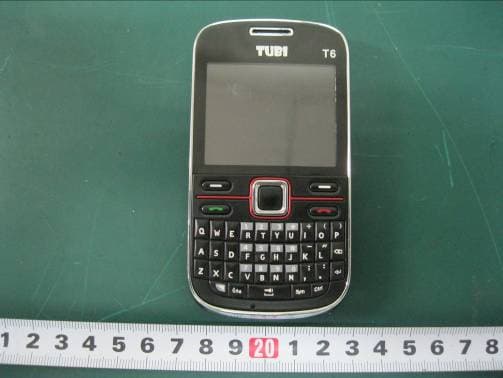
Click to zoom
Application Details
- Equipment Class
- PCE - PCS Licensed Transmitter held to ear
- Date of Grant
- Jul 21, 2011
- Application Purpose
- Original Equipment
- Date of Application
- Jul 21, 2011
- Equipment Note
- GSM Mobile Phone
- Frequency Range
- 1850.20000000 - 1909.80000000
- Company
- BEST MOVIL C.A
- Country
- Venezuela
Documents & Files
Document Text
Text extracted from the exhibit documents filed with the FCC. Open a document above to read the original.
Users Manual
TUBI T6 PRO GSM / GPRS Digital Mobile Phone User’s Guide CONTENTS 1. THE BASICS............................................................................. 6 1.1. INTRODUCTION.................................................................. 73 1.2. SECURITY GUIDE................................................................. 7 1.3. FOR YOUR SAFETY.............................................................. 8 2. BEFORE USE......................................................................... 19 2.1. COMPONENTS NAME AND EXPLANATION........................... 19 2.1.1. Technical Specification.......................................... 14 2.1.2. Introduction to Icons in standby........................... 21 2.2. KEY FUNCTION................................................................... 21 2.3. INSTALL OF SIM CARD, T-FLASH CARD.............................. 24 2.3.1. SIM card.................................................................. 24 2.3.2. Install and Remove the SIM.................................. 25 2.3.3. T-flash card.............................................................. 26 2.4. BATTERY............................................................................ 27 2.4.1. Installation the Battery........................................... 27 2.4.2. Battery charging..................................................... 28 2.5. SECURITY CODE................................................................. 30 3. QUICK START........................................................................ 24 3.1. FEATURE FUNCTION........................................................... 32 3.2. DIALING............................................................................. 27 3.3. REJECT A CALL................................................................... 35 3.4. ANSWER A CALL................................................................ 35 3.5. ENDING A CALL.................................................................. 36 3.6. EMERGENCY CALLS........................................................... 36 3.7. CALL HISTORY................................................................... 36 3.8. CALL DIVERT..................................................................... 36 3.9. CALL WAITING.................................................................... 37 3.10. CALL BARRING................................................................... 37 3.11. POWER OFF........................................................................ 37 4. FUNCTION MENU.................................................................. 38 4.1. FILE MANAGER................................................................... 38 4.2. PHONE BOOK..................................................................... 38 4.3. FUN&GAMES..................................................................... 40 4.4. EXTRA................................................................................ 40 4.4.1. Calculator................................................................ 40 4.4.2. Ebook Reader......................................................... 41 4.4.3. Bluetooth(optional)............................................ 42 4.5. CALL CENTER.................................................................... 45 4.5.1. Call History.............................................................. 46 4.5.2. Call Settings............................................................ 46 4.6. MASSAGES......................................................................... 46 4.6.1. Write Message........................................................ 46 4.6.2. Inbox......................................................................... 37 4.6.3. Outbox..................................................................... 38 4.6.4. MMS......................................................................... 39 4.6.5. Broadcast Message............................................... 51 4.6.6. Te m p l a t e s................................................................ 41 4.6.7. SMS Settings.......................................................... 52 4.7. MULTIMEDIA...................................................................... 43 4.7.1. Camera.................................................................... 53 4.7.2. Image Viewer.......................................................... 54 4.7.3. Video recorder........................................................ 54 4.7.4. Video player............................................................ 54 4.7.5. Audio player............................................................ 55 4.7.6. FM Radio................................................................. 56 4.8. SERVICES........................................................................... 57 4.8.1. STK........................................................................... 57 4.8.2. Internet service....................................................... 57 4.8.3. Data account........................................................... 59 4.9. ORGANIZER........................................................................ 49 4.9.1. Calendar.................................................................. 49 4.9.2. Alarm........................................................................ 61 4.9.3. World clock.............................................................. 62 4.9.4. Flash Light............................................................... 62 4.10. SETTINGS........................................................................... 50 4.10.1. Dual SIM Settings.................................................. 62 4.10.2. Phone settings........................................................ 62 4.10.3. Network Settings.................................................... 51 4.10.4. Security Settings.................................................... 63 4.10.5. Restore Factory Setting......................................... 66 4.11. USER…
Text truncated - open the document above for the full version.
Block Diagram
Simcard Main LCD 2.2" QCIF BASEBAND PROCESSOR MT6223C TF CARD Keypad Matrix 5 Pin Mini USB I/O I/F Audio AMP TRANSCEIVER MT6139 PA SKYWORKS SKY77518 Blueooth RDA5868+ FM Radio RDA5802 MT6302 Speaker R F s e r i a l I / F Headset UART I/F USB 1.1 I/F Sim I/F 16bits Reveiver Microphone UART3 ASM S D I / F control DATA bus Memory_NOR+PSRAM TV00578002AABD YUV DATA 0.3 Mega Camera Module OV Address bus PCM I/F Vibrator 2.5MM Jak DSP SP5369 C o n t r o l B u s IIC I/F Keypad bus
Cover Letter(s)
SCS-F18: Project and Product Certification Representative Authorization Letter Page 1 of 2 Rev 2.0 2206 Ringwood Avenue San Jose, CA 95131 Tel: 408-526-1188 Fax: 408-526-1088 Email: [email protected] Project and Product Certification Representative Authorization Letter Revision History Reason for Amendment (current / obsolete) From To Approved Date Initial Release (current) 1.0 1.0 Nov-14-2006 Revised wording (current) 1.0 2.0 Sept–25-2007
External Photos
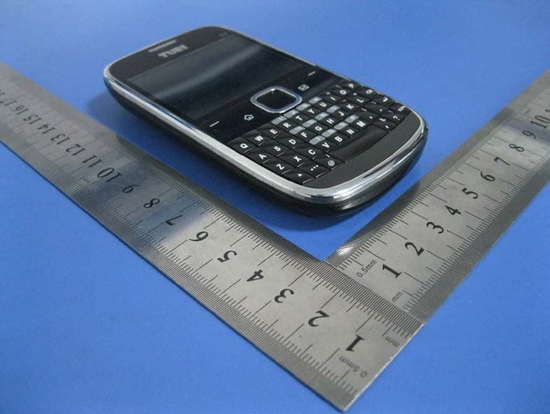
Title: RF Test Report for GSM Mobile Phone Model: T6 To: FCC 15.247:2010 Serial#: 1107008-FCC(BT) Issue Date: 18 July, 2011 Page: 44 of 60 www.siemic.com.cn Annex B. EUT AND TEST SETUP PHOTOGRAPHS Annex B.i. Photograph: EUT External Photo Front View of EUT Rear View of EUT Title: RF Test Report for GSM Mobile Phone Model: T6 To: FCC 15.247:2010 Serial#: 1107008-FCC(BT) Issue Date: 18 July, 2011 Page: 45 of 60 www.siemic.com.cn Left View of EUT Right View of EUT Title: RF Test Report for GSM Mobile Phone Model: T6 To: FCC 15.247:2010 Serial#: 1107008-FCC(BT) Issue Date: 18 July, 2011 Page: 46 of 60 www.siemic.com.cn Top View of EUT Bottom View of EUT Title: RF Test Report for GSM Mobile Phone Model: T6 To: FCC 15.247:2010 Serial#: 1107008-FCC(BT) Issue Date: 18 July, 2011 Page: 47 of 60 www.siemic.com.cn Front View of Power Adapter Front View of PSU Label
Internal Photos
Front View of Main PCB Board Rear View of Main PCB Board GSM Antenna BTAntenna Front View of Power Supply PCB Board Rear View of Power Supply PCB Board Front View of Battery Rear View of Battery Cover off photo GSM Antenna BT Antenna
Operational Description
OPERATIONAL DESCRIPTION OF T6 The equipment under test (EUT) is the transmitter of T6 a Four-band (850/900/1800/1900) GSM/GPRS mobile phone. The transmitter operates in a duplex system according to the GSM standards. The majority of the phone circuitry consists : the SKY77518 Power Amplifier and the MT6223C Baseband Processor. There is also a combination Flash Memory/PSRAM IC. The system is powered by a rechargeable lithium-ion battery with a nominal voltage of 3.7 volts. The receiver consists of two distinct parts, the RF receiver front-end and the IF section. The RF receiver front-end amplifies the GSM850 ( 869-894MHZ), E-GSM900 (925-960 MHz), DCS1800 (1805-1880 MHz), PCS1900( 1930-1990MHZ) aerial signal, converts the chosen channel down to a low IF of 0 kHz, and provides in addition more than 35 dB image suppression. Two LNAs are available on-chip and can be configured to allow 4-band functionality. The switched LNA will be used for roaming in different countries. Some selectivity is provided at this stage by an on-chip low-pass filter, and channel selectivity is provided by means of a high performance integrated band-pass filter. The IF section further amplifies the wanted channel performs gain control to tune the output level to the desired value and rejects DC. This DC rejection is realised with an active high pass circuit and operates either continuously or keeps the acquired offset correction during the burst depending on the programming. The transmitter is fully differential using a direct up conversion architecture. It consists of a single side band power up mixer. Gain is controlled by 4 dB via 3-wire serial bus programming. The fully integrated VCO and the power mixer are designed to achieve LO suppression, quadrature phase error, quadrature amplitude balance and low noise floor specifications. Output balun components are integrated to drive a standard 50 ohms single ended load. The local oscillator (LO) signals required are provided by an on chip VCO for operation of the receive and transmit sections. The VCO is fully integrated and self calibrating to reduce manufacturing tolerances. It consists of 64 differents frequency ranges that are selected internally depending on frequency programming. The frequencies of the RF VCO are set by an internal fractional N synthesiser PLL circuit, which are programmable via a 3-wire serial bus. Comparison frequency is 26 MHz (24 Hz step programmability) derived from the 26 MHz reference signal which is generated from the semi integrated reference oscillator. The quadrature phase RF LO signals required for IQ mixers are generated internally. 26 MHz is the reference frequency. It is turned on when the supply voltage VTCXO is applied. After buffering a reference clock of 26 MHz is supplied to the other parts of the system through the pin XBUF. The circuit can be powered-up into four different modes: RX, TX, SYN or REF mode, depending on supply voltages applied, the logical level at pin CTRL and the 3-wire bus serial programming. In RX (TX) mode, all sections required for receive (transmit) are turned on. The SYN mode is used to power-up the synthesiser and the RF-VCO prior to the RX or TX mode. In the SYN mode, some internal LO buffers are also powered-up such that VCO pulling is minimized when switching on the receiver or the transmitter. The reference oscillator (REF mode) is turned on by applying the supply voltage. Additionally band selection is done using the 3-wire bus serial programming allowing the proper enabling of the LNAs. RF section also includes Bluetooth chips RDA5868+ and FM circuit chips using RDA5802. Device features: Bluetooth Features Compliant with Bluetooth 2.1 Bluetooth Piconet and Scatternet support Meet class 2 and class 3 transmitting power requirement, support class1 operation with external power amplifier NZIF receiver with -90dBm sensitivity FM Receiver Features Support worldwide frequency band ☆ 65 -108 MHz RDA5868+ product line provides two applications for handset and PC. Two different product numbers are used for different usages. Both master and slave operating mode are provided on PCM.interface with programmable data frequency to connect to the. voice channel on the host chip. The UART interface supports.hardware flow control as well as high-speed baud rate.connection. The PTA interface accommodates different.arbitration scheme in which channel utilization can be efficiently.performed in a co-existence environment. The external reference.clock interface supports wide ranges of frequencies that the.mobile phones use. The USB interface supports full-speed device operation. Three outputs are provided to drive RF switches of the phone, e.g. for switching between bands. The baseband processor handles all physical layer radio control signals and network interfaces. The 32 KHz clock oscillator operates the baseband IC from a backup battery when the main battery is removed. The baseband processor is a dual-core device that splits the processing between a DSP core and an ARM ™ processor. The DSP handles the physical and layer 1 processing, while the ARM executes the layer 2 and layer 3 protocol and the man-machine interface (MMI). The dual cores communicate through a dedicated block of dual port memory. It also communicates with the Subscriber Identity Module (SIM) through an interface to the mixed signal device. The baseband processor also communicates to the calibration system or external devices through a digital serial link that is available on the system connector. The other main signals on the system connector include the digital audio interface (DAI) and allows for an external battery charging voltage. The MMI completes the phone design and includes the displays, keypads, vibration motor, speaker, microphone, and headset.
Parts List/Tune Up Info
HC4F8330J CAP_CM1_22PF_+/-5%_50V_CH0402_RO GRM1555C1H330J* MURATA C313,C318,C317 HL3F0102N BEAD_1000R/100MHz_+/-25%_CH0402_RO BK1005HM102-T TAIYO_YUDEN L303,L302 HR1F0102J RES_MF_1KR_+/-5%_1/16W_CH0402_RO RC0402JR-071K YAGEO R512 HR1F0103J RES_MF_10KR_+/-5%_1/16W_CH0402_RO RC0402JR-0710K YAGEO R303 HR1F0104J RES_MF_100KR_+/-5%_1/16W_CH0402_RO RC0402JR-07100K YAGEO R201 HR1F0181J RES_MF_180R_+/-5%_1/16W_CH0402_RO RC0402JR-07180R YAGEO R506,R505,R504 HR2F30011 VARISTOR_5.6V_60PF_CH0402_RO ICVL0505600V150 ICT V303,V501,V306,V305 MR4001491 PCB F96 MAINBOARD HDIPCB P1.0 4L RO F96_MB_P1.0 YLAD PCB801 HH1S00291 LED_WRITE_SIDE_3.8*0.6*1.2_R0 AOT-3806PW21B-N10-X-3-M AOT LED502,LED501 EX3000231 CON_SIM_H1.5_BRIDGE_R0 CAF99-06153-1503 LCN NA EX5000291 CON_BAT_3PIN_H4.2_P3.75_Z_R0 BA71G331A-R D&D NA EX6000071 CON_USB_5PIN_H2.5_RO UAF95-05254-1500 LCN NA EX8000051 CON_Audio_Jack_6PIN_D2.5_RO SM-JAK06-001 SABER NA HC1F4105K CAP_CM2_1uF_X5R_10%_6.3V_CH0402_RO GRM155R60J105K* MURATA NA HC1F4224K CAP_CM2_220NF_+/-10%_6.3V_CH0402_RO GRM155R60J224K* MURATA NA HC1F5104K CAP_CM2_100NF_+/-10%_10V_CH0402_RO GRM155R71A104K* MURATA NA HC1G4105K CAP_CM2_1UF_+/-10%_6.3V_CH0603_RO GRM188R60J105K* MURATA NA HC1G4475K CAP_X5R_4.7UF_+/-10%_6.3V_CH0603_RO GRM188R60J475K* MURATA NA HC1G5225K CAP_CM2_2.2UF_+/-10%_10V_CH0603_RO GRM188R61A225K* MURATA NA HC1H6226Z CAP_CM2_22UF_+80%-20%_6.3V_CH0805_RO GRM21BR60J226ME39L MURATA NA HC2F6103K CAP_CM2_10NF_+/-10%_16V_CH0402_RO GRM155R71C103K MURATA NA HC2F6223K CAP_CM2_22NF_+/-10%_16V_CH0402_RO GRM155R71C223K* murata NA HC2F8102K CAP_CM2_1NF_+/-10%_50V_CH0402_RO GRM155R71H102K* MURATA NA HC4F8101J CAP_CM1_100PF_+/-5%_50V_CH0402_RO GRM1555C1H101J* MURATA NA HC4F8220J CAP_CM1_22PF_+/-5%_50V_CH0402_RO GRM1555C1H220J* MURATA NA HC4F8270J CAP_CM1_27PF_5%_50V_CH0402_RO GRM1555C1H270J* MURATA NA HC6V4107M CAP_STA_100UF_+/-20%_6.3V_C3528_RO F930J107MBA Nichicon NA HD2S00021 MOSFET_and_Schottky_Diode_TSOP-6_RO TT8U2TR ROHM NA HG1S00021 CRY_XO_32.768K_CH_RO SSP-T7-F Seiko NA HL1F0104J IND_HIGH_100NH_+/-5%_CH0402_RO LQG15HSR10J02D MURATA NA HR1F0000J RES_MF_0R_1A_CH0402_RO RC0402JR-070R YAGEO NA HR1F0101J RES_MF_100R_+/-5%_1/16W_CH0402_RO RC0402JR-07100R YAGEO NA HR1F0152J RES_MF_1.5KR_+/-5%_1/16W_CH0402_RO RC0402JR-071K5 YAGEO NA HR1F0222J RES_MF_2K2R_+/-5%_1/16W_CH0402_RO RC0402JR-072K2L YAGEO NA HR1F0240J RES_MF_24R_+/-5%_1/16W_CH0402_RO RC0402JR-0724R YAGEO NA HR1F0243J RES_MF_24KR_+/-5%_1/16W_CH0402_RO RC0402JR-0724KL YAGEO NA HR1F0392J RES_MF_3K9R_+/-5%_1/16W_CH0402_RO RC0402JR-073K9 YAGEO NA HR1F0473J RES_MF_47KR_+/-5%_1/16W_CH0402_RO RC0402JR-0747K YAGEO NA HR1F0474J RES_MF_470KR_+/-5%_1/16W_CH0402_RO RC0402JR-07470K YAGEO NA HR1H0222J RES_MF_0.22R_+/-5%_0.125W_CH0805_RO RL0805JR-070R22L YAGEO NA HR2F30031 TVS_5V_50pF_SP_CH0402_RO ESD9X5V-2/TR WILL NA HR2G40011 VARISTOR_18V_100PF_CH0603_RO ICVL1018101A400 ICT NA HV1S00011 DIO_Schottky_Barrier_RO RB521S-30TE61 ROHM NA HW1S00621 IC_MT6223D_GSM/GPRS_BB_PROCESSOR_RO MT6223D MTK NA HW3S00121 IC_AUDIO_CLASSAB_CSP_R0 SGM4890YG/TR SGMC NA MR3001571 SH_0I7_RF_PA_COVER_10.5*10.3*1.5_R0 徕木 NA MR3001751 SH_096_RF_TRC_COVER_19.95*13.8*1.45_RO 徕木 NA MR3001741 SH_096_BT_COVER_13*9.6*1.45_RO 徕木 NA MR3001731 SH_096_BB-CVOER_47*28*1.6_RO 徕木 NA HC1F4105K CAP_CM2_1uF_X5R_10%_6.3V_CH0402_RO GRM155R60J105K* MURATA NA HC1F5104K CAP_CM2_100NF_+/-10%_10V_CH0402_RO GRM155R71A104K* MURATA NA HC1G4475K CAP_X5R_4.7UF_+/-10%_6.3V_CH0603_RO GRM188R60J475K* MURATA NA HC2F8102K CAP_CM2_1NF_+/-10%_50V_CH0402_RO GRM155R71H102K* MURATA NA HC4F8100D CAP_CM1_10PF_0.5PF_50V_CH0402_RO GRM1555C1H100D* MURATA NA HC4F8101J CAP_CM1_100PF_+/-5%_50V_CH0402_RO GRM1555C1H101J* MURATA NA HC4F8470J CAP_CM2_47PF_+/-5%_50V_CH0402_RO GRM1555C1H470J* MURATA NA HL1F0392S IND 3.9NH +/-0.3NH CH0402_RO LQG15HS3N9S02D MURATA NA HW4S00051 IC_BT_QFN40_RO RDA5868+ RDA NA HZ5S00021 IC_BAND_PASS_FILTER_2.45G_RO TBF1608245R2* CYNTEC NA HC1F4105K CAP_CM2_1uF_X5R_10%_6.3V_CH0402_RO GRM155R60J105K* MURATA NA HC1F5104K CAP_CM2_100NF_+/-10%_10V_CH0402_RO GRM155R71A104K* MURATA NA HC2F8221K CAP_CM2_220PF_+/-10%_50V_CH0402_RO GRM155R71H221K* MURATA NA HD4S00011 PMIC_Dual_LDO_1.8V+2.8V_SOT26W_RO PAM3102-AST26R1 PAM NA HD4S00061 PMIC_LDO_3.3V(pull_down)_SOT25_RO XC6219A332MR TOREX NA HL1F0223J IND_HIGH_22NH_+/-5%_CH0402_RO LQG15HN22NJ02D Murata NA HR1F0000J RES_MF_0R_1A_CH0402_RO RC0402JR-070R YAGEO NA HR1F0103J RES_MF_10KR_+/-5%_1/16W_CH0402_RO RC0402JR-0710K YAGEO NA HR1F0473J RES_MF_47KR_+/-5%_1/16W_CH0402_RO RC0402JR-0747K YAGEO NA HZ5S00131 IC_Quad_SPDT_Analog_SWITCH_SC70-6_RO SGM3157YC6/TR SGMC NA HW1S00631 IC_DSP_LQFP64_RO SP5369 SuperPix NA HM4S00181 IC_Memory_NOR+PSRAM_FBGA_64+32_1.8V_RO FM91D06432UNA ESMT NA HR1F0000J RES_MF_0R_1A_CH0402_RO RC0402JR-070R YAGEO NA HM4S00191 IC_Memory_NOR+PSRAM_FBGA_64+32_2.8V_RO K5L6331CAA-D270 SAMSUNG NA HR1F0000J RES_MF_0R_1A_CH0402_RO RC0402JR-070R YAGEO NA HC1F4105K CAP_CM2_1uF_X5R_10%_6.3V_CH0402_RO GRM155R60J105K* MURATA NA HC1F5104K CAP_CM2_100NF_+/-10%_10V_CH0402_RO GRM155R71A104K* MURATA NA HC2F7103K CAP_CM2_10NF_+/-10%_25V_CH0402_RO GRM155R71E103K* MURATA NA HC2F8102K CAP_CM2_1NF_+/-10%_50V_CH0402_RO GRM155R71H102K* MURATA NA HC4F8151J CAP_CM1_150PF_+/-5%_50V_CH0402_RO GRM1555C1H151J MURATA NA HL3F0102N BEAD_1000R/100MHz_+/-25%_CH0402_RO BK1005HM102-T TAIYO_YUDEN NA HW1S00411 IC_FMRadio_QFN24_RO RDA5802 RDA NA HR1F0000J RES_MF_0R_1A_CH0402_RO RC0402JR-070R YAGEO NA HC1F4105K CAP_CM2_1uF_X5R_10%_6.3V_CH0402_RO GRM155R60J105K* MURATA NA HC1G4475K CAP_X5R_4.7UF_+/-10%_6.3V_CH0603_RO GRM188R60J475K* MURATA NA HC4F8330J CAP_CM1_33PF_+/-5%_50V_CH0402_RO GRM1555C1H330J* MURATA NA HR1F0104J RES_MF_100KR_+/-5%_1/16W_CH0402_RO RC0402JR-07100K YAGEO NA HR1F0243J RES_MF_24KR_+/-5%_1/16W_CH0402_RO RC0402JR-0724KL YAGEO NA HR1F0473J RES_MF_47KR_+/-5%_1/16W_CH0402_RO RC0402JR-0747K YAGEO NA HR2F30011 VARISTOR_5.6V_60PF_CH0402_RO ICVL0505600V150 ICT NA HW3S00121 IC_AUDIO_CLASSAB_CSP_R0 SGM4890YG/TR SGMC NA HR1F0000J RES_MF_0R_1A_CH0402_RO RC0402JR-070R YAGEO NA HC1F4…
Text truncated - open the document above for the full version.
Parts List/Tune Up Info
There is no Tune up procedure for RF power. Rated Peak RF power output : GSM 850 , 32.5dBm ±0.7 PCS1900 , 27.5dBm ± 0.7 Then these appropriate rated RF output power settings are stored in each device individually. The user has no possibility to change these settings later on, and during manufacturing each device will be individual calibrated. The measurement is done in fully calibrated setup, which is based on the base station simulator. Furthermore, the highest power level is verified afterwards in a call measurement on three channels (low, middle and high).
RF Exposure Info
BEST MOVIL C.A GSM MOBILE PHONE Model: T6 July 03rd, 2011 Report No.: 1107008-FCC(SAR) Rev1.0 (This report supersedes 1107008-FCC(SAR)) This Test Report is Issued Under the Authority of: David Zhang Compliance Engineer Leslie Bai Director of Certification Modifications made to the product : None This test report may be reproduced in full only. All Test Data Presented in this report is only applicable to presented Test sample. Title: RF Test Report of Shenzhen Phone-Talk Technology Co.,Ltd Model : T6 To C95.1, IEEE 1528, OET Bulletin 65 Supplement C & RSS-102 Issue 4 and Safety Code 6 Serial# 1107008-FCC(SAR) Rev1.0 Issue Date July 03rd, 2011 Page 2 of 91 www.siemic.com REDIT SIEMIC SIEM Laboratory Introduction ATION SIEMIC, headquartered in the heart of Silicon Valley, with superior facilities in US and Asia, is one of the leading independent testing and certification facilities providing customers with one-stop shop services for Compliance Testing and Global Certifications. In addition to testing and certification, SIEMIC provides initial design reviews and compliance management through out a project. Our extensive experience with China , Asia Pacific, North America, European, and international compliance requirements, assures the fastest, most cost effective way to attain regulatory compliance for the global markets . Accreditations for Conformity Assessment Country/Region Accreditation Body Scope USA FCC, A2LA EMC , RF/Wireless , Telecom , SAR Canada IC, A2LA, NIST EMC, RF/Wireless , Telecom , SAR Taiwan BSMI , NCC , NIST EMC, RF, Telecom , Safety Hong Kong OFTA , NIST RF/Wireless ,Telecom Australia NATA, NIST EMC, RF, Telecom , Safety Korea KCC/RRA, NIST EMI, EMS, RF , Telecom, Safety , SAR Japan VCCI, JATE, TELEC, RFT EMI, RF/Wireless, Telecom Mexico NOM, COFETEL, Caniety Safety, EMC , RF/Wireless, Telecom Europe A2LA, NIST EMC, RF, Telecom , Safety, SAR Accreditations for Product Certifications Country Accreditation Body Scope USA FCC TCB, NIST EMC , RF , Telecom Canada IC FCB , NIST EMC , RF , Telecom Singapore iDA, NIST EMC , RF , Telecom EU NB EMC & R&TTE Directive Japan MIC, (RCB 208) RF , Telecom HongKong OFTA (US002) RF , Telecom Title: RF Test Report of Shenzhen Phone-Talk Technology Co.,Ltd Model : T6 To C95.1, IEEE 1528, OET Bulletin 65 Supplement C & RSS-102 Issue 4 and Safety Code 6 Serial# 1107008-FCC(SAR) Rev1.0 Issue Date July 03rd, 2011 Page 3 of 91 www.siemic.com This page has been left blank intentionally. Title: RF Test Report of Shenzhen Phone-Talk Technology Co.,Ltd Model : T6 To C95.1, IEEE 1528, OET Bulletin 65 Supplement C & RSS-102 Issue 4 and Safety Code 6 Serial# 1107008-FCC(SAR) Rev1.0 Issue Date July 03rd, 2011 Page 4 of 91 www.siemic.com CONTENTS 1 EXECUTIVE SUMMARY & EUT INFORMATION...............................................................................................................6 2 TECHNICAL DETAILS.....................................................................................................................................................7 3 INTRODUCTION..............................................................................................................................................................8 4 SAR MEASUREMENT SETUP.........................................................................................................................................9 5 ANSI/IEEE C95.1 – 1999 RF EXPOSURE LIMIT.............................................................................................................19 6 SYSTEM AND LIQUID VALIDATION..............................................................................................................................20 7 TYPE A MEASUREMENT UNCERTAINTY.....................................................................................................................25 8 OUTPUT POWER VERIFICATION..................................................................................................................................27 9 SAR TEST RESULTS....................................................................................................................................................28 ANNEX A. TEST INSTRUMENT & METHOD...........................................................................................................................43 ANNEX B EUT AND TEST SETUP PHOTOGRAPHS..............................................................................................................45 ANNEX C CALIBRATION REPORTS.....................................................................................................................................48 Title: RF Test Report of Shenzhen Phone-Talk Technology Co.,Ltd Model : T6 To C95.1, IEEE 1528, OET Bulletin 65 Supplement C & RSS-102 Issue 4 and Safety Code 6 Serial# 1107008-FCC(SAR) Rev1.0 Issue Date July 03rd, 2011 Page 5 of 91 www.siemic.com This page has been left blank intentionally. Title: RF Test Report of Shenzhen Phone-Talk Technology Co.,Ltd Model : T6 To C95.1, IEEE 1528, OET Bulletin 65 Supplement C & RSS-102 Issue 4 and Safety Code 6 Serial# 1107008-FCC(SAR) Rev1.0 Issue Date July 03rd, 2011 Page 6 of 91 www.siemic.com 1 Executive Summary & EUT information The purpose of this test programmed was to demonstrate compliance of the Shenzhen Phone-Talk Technology Co.,Ltd Model: T6 against the current Stipulated Standards. The GSM Mobile Phone have demonstrated compliance with the C95.1 , IEEE 1528, OET Bulletin 65 Supplement C , RSS-102 Issue 4 and Safety Code 6. The test has demonstrated that this unit complies with stipulated standards. EUT Information EUT Description : GSM Mobile Phone Model No : T6 Serial No : N/A HW version : N/A IMEI : IMEI 1: 358865038940583 IMEI 2: 358865038961383 Input Power : 3.6-4.2VDC 950mAh Maximum Conducted Output Power to Antenna GSM850(Class 4) : 2.01 W (33.23dBm) GPRS850(Multislot Class 10) : 1.98 W (32.97 dBm) GSM1900 (Class 1) : 0.64 W (28.08 dBm) GPRS1900 (Multislot Class 10) : …
Text truncated - open the document above for the full version.
Schematics
I N 1 O U T 1 I N 2 O U T 2 O U T B 2 G N D O U T B 1 G N D O U T B GND I N O U T GND O U T B GND I N O U T GND D r a w i n g N u m b e r : 6 7 T I T L E : Q A C H K : P a g e : S i z e : R E V : 3 2 1 4 5 4 5 BC l o g i c A 3 1 2 6 8 B P O I N T P O I N T - P r o p r i e t a r y 3 CD 7 T i m e C h a n g e d : E n g i n e e r : EF A D a t e C h a n g e d : D 8 D r a w n b y : R & D C H K : D O C C T R L C H K : M F G E N G R C H K : A EF C h a n g e d b y : z h u o j i a n f a n g F r i d a y , S e p t e m b e r 2 8 , 2 0 0 7 5 : 2 2 : 3 4 p m Z H U O J I A N F A N G Z H U O J I A N F A N G 1 123 456 0 R R 1 1 3 C 1 0 6 7 p A S 1 7 9 - 9 2 U 1 1 0 C 1 3 4 7 p C 1 4 8 1 K R 1 0 4 6 p R 1 0 5 1 5 K 3 45 2 - E 1 , 3 - E 4 , 5 - A 1 , 6 - B 2 , 7 - B 5 1 - B 5 , 2 - B 2 1 - B 5 , 2 - B 2 1 - C 6 X C 6 2 0 4 2 . 8 V U 1 0 6 1 2 L 1 0 7 7 5 R / 1 0 0 M h z C 1 2 0 1 0 0 n 1 0 0 n C 1 3 1 6 p C 1 3 3 R 1 0 1 1 0 R 2 2 p C 1 4 3 C 1 1 3 1 0 0 n 1 0 0 n C 1 1 4 1 0 K 1 u C 1 1 2 2 2 0 p C 1 3 9 R 1 0 6 6 p 1 K R 1 1 1 C 1 3 0 C 1 4 1 1 . 5 p 2 - D 2 1 . 5 p C 1 3 8 2 - C 2 2 - C 2 6 p L 1 1 8 1 - B 7 , 2 - F 2 3 - A 4 2 - C 2 1 . 8 p C 1 2 2 X 1 n L 1 0 9 C 1 1 1 1 n A N T 1 0 2 4 . 7 u C 1 1 0 C 1 0 9 3 3 p C 1 0 8 1 u 1 0 0 n C 1 1 9 C 1 1 8 1 u U 1 0 2 A S 1 7 9 - 9 2 123 456 U 1 0 9 S A F E A 1 . 9 6 G 1 2 34 5 1 0 n C 1 3 5 2 3 4 5 6 A N T 1 0 1 R 1 0 3 0 R J 1 0 1 M M 8 4 3 0 - 2 6 1 0 R B 3 1 6789 X C 1 2 5 0 . 5 p B 9 5 0 1 U 1 0 4 1 10 2 3 4 5 L 1 0 5 7 5 R / 1 0 0 M h z C 1 2 4 1 0 n L 1 1 7 6 p 1 u C 1 1 6 C 1 1 7 1 u C 1 0 4 C 1 1 5 1 n C 1 0 1 1 8 p 1 8 p 1 . 5 n L 1 0 4 1 5 n L 1 0 1 38 39 4 40 56789 2 8 2 9 3 3 0 31 32 33 34 35 36 37 18 19 2 20 2 1 2 2 2 3 2 4 2 5 2 6 2 7 U 1 0 1 11 0 11 12 13 14 15 16 17 M T 6 1 3 9 B N 2 2 p C 1 0 7 1 0 0 u C 1 2 8 7 8 9 2 2 n L 1 0 2 16 1 7 18 1 9 2 20 21 345 6 U 1 0 3 S K Y 7 7 5 1 8 1 10 11 12 13 14 15 L 1 1 3 3.9n C 1 0 5 7 p 1 - A 6 , 3 - B 6 , 4 - A 7 , 5 - A 6 , # 3 0 . 5 p C 1 4 5 X R 1 1 0 0 R 3 - B 4 L 1 1 0 1-B4, 2-D4,3-A7 ,4-B6,#3 1 - A 6 , 2 - D 4 , 3 - A 7 , 4 - B 6 , # 3 1 . 5 p C 1 3 2 6 . 8 n 34 5 C 1 2 3 0 . 5 p S A F E A 8 8 1 . 5 M U 1 0 7 1 2 C 1 2 6 2 . 2 u C 1 2 7 2 . 2 u 4 . 7 n L 1 1 4 7 5 R / 1 0 0 M h z L 1 1 6 3 9 p C 1 5 0 O S C 1 0 1 12 34 1-B8 R 1 1 2 0 R T S T 2 6 M 2 - A 3 1 8 n L 1 0 8 3 - A 4 C 1 2 9 C 1 4 0 1 8 p L 1 1 2 1 5 n 1 8 p 1 0 0 K R 1 0 7 L 1 0 3 1 . 5 n C 1 2 1 1 0 0 n 2 2 p C 1 4 2 1 - B 8 1 - B 8 1 - B 8 1-B8 7 p C 1 4 7 L 1 0 6 4 . 7 n 2 - A 3 L 1 1 1 7 5 R / 1 0 0 M h z X U 1 0 8 L F L 1 5 1 . 8 1 G 1 23 4 3 - A 4 R 1 0 9 1 K 2 2 p C 1 0 3 C 1 3 7 1 0 0 n C 1 0 2 4 7 p 3 - A 4 2 - C 2 3 - A 4 G S M 8 5 0 _ R X G S M 8 5 0 _ R X G S M 9 0 0 _ R X B A N D S W _ D C S G S M 9 0 0 _ R X V B A T V C X O E N B T 2 6 M H Z V A P C P A _ E N 2 6 M H Z V B A T VBA T V C X O E N V C C R F VCC RF VCC RF V C C R F V C C R F V C C R F V A F C V D D V C X O E N R F V C O E N S D A T A S C L K L E Q B QI B I CDE 6 7 R 2 0 7 F O R 2 . 8 V M E M O R Y 7 5 A D E R & D C H K : S i z e : T I T L E : F M T 6 2 2 3 _ A B D 3 AB 8 A D O C C T R L C H K : M F G E N G R C H K : A BCDEF P O I N T - P r o p r i e t a r y C h a n g e d b y : D a t e C h a n g e d : T i m e C h a n g e d : B E n g i n e e r : D r a w n b y : C 5 4 6 7 2 6 7 8 1 P O I N T F 1 2 3 4 2 3 4 5 2 6 C D Q A C H K : R E V : D r a w i n g N u m b e r : P a g e : 5 1 E R 2 0 3 F O R 1 . 8 V M E M O R Y 1 4 l o g i c A 3 Z H U O J I A N F A N G Z H U O J I A N F A N G 5 : 2 5 : 0 6 p m F r i d a y , S e p t e m b e r 2 8 , 2 0 0 7 z h u o j i a n f a n g 2 B 8 F 3 8 C 2 0 2 4 . 7 u 4 - E 4 2 - E 7 , …
Text truncated - open the document above for the full version.
Contact Information
Applicant
Simon Molero(Director)
Test Firm
SIEMIC (Nanjing-China) LaboratoriesLeslie Bai
Technical Specifications
| # | Rule Parts | Frequency Range | Power Output | Emission | Tolerance |
|---|---|---|---|---|---|
| 2 | 24E | 1.85 GHz - 1.91 GHz | 510.00 mW | 250KG7W | 70 Hz |
Other Applications from BEST MOVIL C.A
ZQYTUBIT7
Jan 14, 2012GSM Mobile Phone
Equipment Class
PCE - PCS Licensed Transmitter held to ear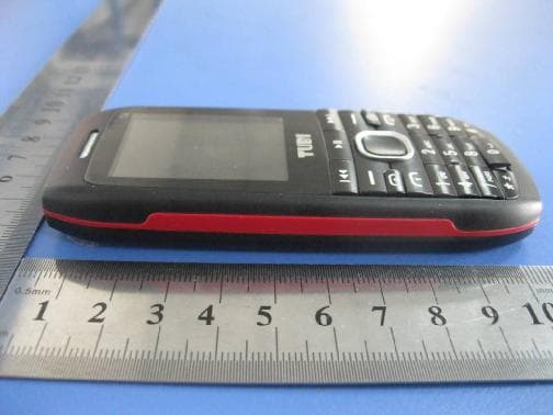
ZQYTUBIT4
Dec 26, 2011GSM Mobile Phone
Equipment Class
DSS - Part 15 Spread Spectrum Transmitter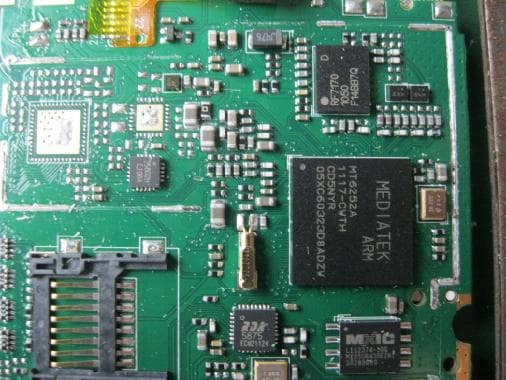
ZQYTUBIT5
Oct 20, 2011GSM Mobile Phone
Equipment Class
PCE - PCS Licensed Transmitter held to ear